メモリ価格は日々変動しています — サイト上の価格は市場に遅れている可能性があります。最新の見積もりについてはRFQを送信してください。
最新価格をリクエスト →
SK hynix

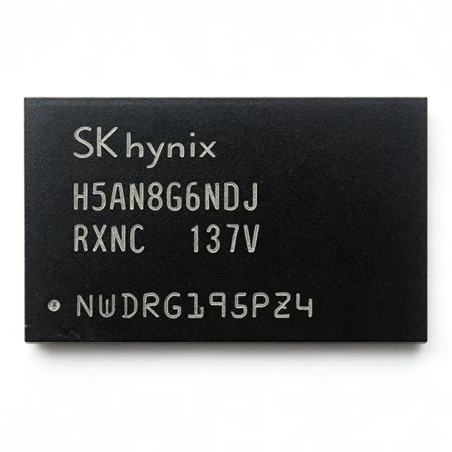
H5AN8G6NDJR-XNC - 8Gb DDR4-3200 x16 DRAM | SK Hynix

部品番号: H5AN8G6NDJR-XNC ✓ 生産中
在庫あり 1〜3営業日以内に発送
1.2 V (max 1.26 V) Vdss FBGA-96 (13x7.5 mm) Package DDR4 SDRAM Memory
開始価格 $55.6818 USD / 個
MOQ: 1 |
価格更新日: 2026-08-21
ボリューム価格
数量 単価 小計
1 $95.4545 $95.45
10 $68.9394 $689.39
100 $60.9848 $6,098.48
500 $58.3333 $29,166.65
1,000 $55.6818 $55,681.80
ℹ️ すべての価格はUSDです

H5AN8G6NDJR-XNC 概要

The SK Hynix H5AN8G6NDJR-XNC is an 8Gb CMOS Double Data Rate IV (DDR4) Synchronous DRAM organized as 512M x16, operating at a data rate of 3200 Mbps (DDR4-3200). It is housed in a 96-ball FBGA package (13x7.5 mm) and is designed for main memory applications requiring high density and bandwidth. The device supports a supply voltage of 1.2V (VDD) with a maximum of 1.26V, and features auto self-refresh, auto precharge, data mask, dynamic on-chip termination (DTC), ZQ calibration, CRC, write leveling, and asynchronous reset functions.

DDR4 SDRAM is a type of volatile random-access memory that transfers data on both edges of the clock, doubling the data rate compared to DDR3. It operates at lower voltages (1.2V) and higher speeds, making it essential for modern computing systems, servers, and embedded applications. As a memory IC, it falls under the hierarchy of DRAM -> SDRAM -> DDR4 -> memory IC -> semiconductor, and is a critical component for data storage and processing.

Key features include a 512M x16 organization, 3200 Mbps data rate, 1.2V supply, and a 96-ball FBGA package. The device supports various functions such as auto self-refresh and ZQ calibration, which enhance reliability and signal integrity. The x16 interface allows for high bandwidth per chip, making it suitable for applications requiring wide data paths.

Technically, the H5AN8G6NDJR-XNC uses a CMOS process and is fully synchronous, with a differential clock (CK_t/CK_c) and on-die termination for improved signal quality. It supports burst lengths of 8 and 4, and includes a programmable read latency (RL) and write latency (WL) for system optimization. The device also features a temperature-compensated self-refresh (TCSR) to reduce power consumption.

Typical applications include laptop and desktop memory upgrades, industrial controllers, networking equipment, and embedded systems. Its high density and speed make it ideal for applications requiring large memory capacity and fast data access, such as AI edge devices and high-performance computing.

When designing with this component, ensure proper decoupling capacitors near the VDD and VDDQ pins, and follow the PCB layout guidelines for DDR4 routing to maintain signal integrity. The device is RoHS compliant and lead-free, making it suitable for environmentally conscious designs.

ドロップイン代替品: H5AN8G6NDJR-XNC — 同一パッケージでピン互換。PCBの作り直しが必要な異なるパッケージの部品は除外されています。

このシリーズのバリエーション

同一シリーズでドロップイン互換のモデル: H5AN8G6NDJR-XNC (同一形状・フットプリント) — 相違点: Package, Data Rate, CAS Latency, Interface, Burst Length.

Alliance Memory
Package: 96-FBGA (7.5x13)
Data Rate: 2666 Mbps
Interface: POD
比較対象 H5AN8G6NDJR-XNC →
Alliance Memory
Package: 96-FBGA (7.5x13 mm)
Data Rate: 1600 MHz (3200 Mbps)
CAS Latency: 18 ns
比較対象 H5AN8G6NDJR-XNC →
Alliance Memory
Package: 96-FBGA (7.5x13mm)
Data Rate: 3200 Mbps per pin
CAS Latency: Programmable (e.g., 22 cycles)
比較対象 H5AN8G6NDJR-XNC →
SK hynix
Package: 96-ball FBGA (13mm x 7.5mm)
Data Rate: 3200 Mbps (DDR4-3200)
CAS Latency: 22 cycles (at 3200 Mbps)
比較対象 H5AN8G6NDJR-XNC →
SK hynix
Package: FBGA-96 (13x7.5 mm)
比較対象 H5AN8G6NDJR-XNC →
SK hynix
Package: FBGA-78 (7.5x11 mm)
Data Rate: 3200 MT/s
CAS Latency: 22 (typical)
比較対象 H5AN8G6NDJR-XNC →
Samsung Electronics
Package: 78-ball FBGA
Data Rate: 2400 Mbps
Burst Length: 8 and 4
比較対象 H5AN8G6NDJR-XNC →
Samsung Electronics
Package: 78-ball FBGA
Data Rate: 2400 Mbps
比較対象 H5AN8G6NDJR-XNC →
Samsung Electronics
Package: 78-FBGA
CAS Latency: 22 (CL22)
Interface: POD-12
比較対象 H5AN8G6NDJR-XNC →
Samsung Electronics
Package: 96-ball FBGA (9mm x 13mm)
Data Rate: 2400 Mbps
CAS Latency: Programmable (e.g., 16, 17, 18)
比較対象 H5AN8G6NDJR-XNC →
Micron Technology
Package: 78-FBGA (7.5x11 mm)
Data Rate: 2666 MT/s
Interface: Parallel
比較対象 H5AN8G6NDJR-XNC →
Micron Technology
Package: 96-FBGA (8x14)
Data Rate: 2666 MT/s
Interface: Parallel
比較対象 H5AN8G6NDJR-XNC →

クイック比較ツール — 並列比較する代替部品を選択:

H5AN8G6NAFR-UHC

SK hynix
DDR4 SDRAM · 8 Gb · 512M x 16 · 1.2 V · 2400 MT/s · FBGA-96 · 0°C to +85°C · 96

✓ 在庫あり

$5.7422 / 個

データシートを見る →

K4A8G165WB-BCTD

Samsung Electronics
DDR4 SDRAM · 512M x 16 · 8 Gb · 2666 Mbps/pin (PC4-2666) · 1.2 V · 96-ball FBGA · 0°C to +95°C (TC)

✓ 在庫あり

$37 / 個

データシートを見る →

K4A8G165WB-BCRC

Samsung Electronics
DDR4 SDRAM (DRAM, volatile) · 8 Gb (1 GB) · 512M x 16 · 2400 Mbps (PC4-19200) · 1.2 V (1.14 V to 1.26 V) · CMOS DRAM, Samsung 8Gb B-die · 96-ball FBGA (PBGA96) · 0.8 mm

✓ 在庫あり

$12.57 / 個

データシートを見る →

MT40A512M16TB-062E:R

Micron Technology
DDR4 SDRAM · 8 Gbit (512M x 16) · 3200 MT/s · 1600 MHz · 22 · 1.2V ±60mV · 2.5V (-125mV, +250mV) · 0°C to +95°C

✓ 在庫あり

$60 / 個

データシートを見る →

H5AN8G6NCJR-XNC

Same 8Gb x16 DDR4-3200, likely same die, different speed grade suffix

📋 参考代替品(カタログ未掲載)

H5AN8G4NCJR-XNC

8Gb x4 organization, same package, different data bus width

📋 参考代替品(カタログ未掲載)

H5AN8G6NDJR-XNC 最大定格&電気的特性

メモリタイプ DDR4 SDRAM
メモリサイズ 8 Gb
Memory Organization 512M x16
データレート 3200 Mbps
Supply Voltage (VDD) 1.2 V (max 1.26 V)
パッケージ FBGA-96 (13x7.5 mm)
Number of Terminals 96
Maximum Operating Temperature 85 °C
Input/Output Type COMMON
RoHS Compliant
Lead-Free Yes
ハロゲンフリー Yes
Auto Self-Refresh Yes
Auto Precharge Yes
Data Mask Yes
Dynamic On-Chip Termination Yes
ZQ Calibration Yes
CRC Function Yes
Write Leveling Yes
Asynchronous Reset Yes

H5AN8G6NDJR-XNC ピン構成

Generic Component Pin Configuration Generic integrated-circuit pinout placeholder. Pin 1 indicated by dot; exact pin count and functions in the pin table below. 1 N 2 N-1 3 N-2 4 N-3 Pin Configuration See pin table below for pin functions Package-specific diagram not available
ピン A1 VDD — Power supply
ピン A2 DQ0 — Data input/output 0
ピン A3 DQ1 — Data input/output 1
ピン B1 VSS — Ground
ピン B2 DQ2 — Data input/output 2
ピン B3 DQ3 — Data input/output 3
ピン C1 VDDQ — I/O power supply
ピン C2 DQ4 — Data input/output 4
ピン C3 DQ5 — Data input/output 5
ピン D1 VSSQ — I/O ground
ピン D2 DQ6 — Data input/output 6
ピン D3 DQ7 — Data input/output 7
ピン E1 CK_t — Clock (true)
ピン E2 CK_c — Clock (complement)
ピン E3 CKE — Clock enable
ピン F1 CS_n — Chip select
ピン F2 RAS_n — Row address strobe
ピン F3 CAS_n — Column address strobe
ピン G1 WE_n — Write enable
ピン G2 A0 — Address input 0
ピン G3 A1 — Address input 1

主な用途

H5AN8G6NDJR-XNC の用途: 6 件s: Laptop Memory Upgrade, Industrial Controllers, Networking Equipment, Embedded Systems, Data Storage Systems, Consumer Electronics.

📱

Laptop Memory Upgrade

The H5AN8G6NDJR-XNC is an 8Gb x16 DDR4-3200 chip commonly used in laptops for memory upgrades. Its 3200 Mbps data rate and 1.2V operation provide high performance with low power consumption. The x16 interface simplifies PCB layout in space-constrained designs, making it ideal for thin and light notebooks. When upgrading, ensure compatibility with the system's memory controller and support for DDR4-3200 speed.

🏭

Industrial Controllers

In industrial controllers, the H5AN8G6NDJR-XNC provides reliable high-density memory for data logging and real-time processing. Its auto self-refresh and ZQ calibration ensure stable operation over temperature variations. The 8Gb density allows for extended data buffering, while the 3200 Mbps speed supports fast data acquisition. The FBGA-96 package is suitable for compact industrial PCBs.

🌐

Networking Equipment

The H5AN8G6NDJR-XNC is used in routers and switches for packet buffering and routing tables. Its high bandwidth (3200 Mbps) and low latency are critical for network throughput. The x16 organization provides a wide data path, reducing the number of chips needed. The device's CRC function enhances data integrity, which is essential for reliable network communication.

🧩

Embedded Systems

For embedded systems, the H5AN8G6NDJR-XNC offers a balance of density and speed. Its 8Gb capacity supports complex applications like real-time operating systems and edge computing. The 1.2V supply reduces power consumption, extending battery life in portable devices. The device's small FBGA-96 package is ideal for space-constrained designs.

🖥️

Data Storage Systems

In data storage systems, the H5AN8G6NDJR-XNC serves as cache memory for SSDs and RAID controllers. Its high speed (3200 Mbps) and low latency improve I/O performance. The 8Gb density allows for large cache sizes, reducing the need for frequent disk access. The device's auto self-refresh helps maintain data integrity during idle periods.

📺

Consumer Electronics

The H5AN8G6NDJR-XNC is used in smart TVs, set-top boxes, and gaming consoles for system memory. Its 3200 Mbps data rate supports high-resolution video streaming and gaming. The x16 interface simplifies PCB design, reducing manufacturing costs. The device's low power consumption is beneficial for energy-efficient consumer devices.

What is the memory size of H5AN8G6NDJR-XNC?
The H5AN8G6NDJR-XNC has a memory size of 8Gb (gigabits), organized as 512M x16. According to the SK Hynix datasheet, this DDR4 SDRAM provides high density for main memory applications. The x16 organization means 16 data lines, offering high bandwidth per chip.
What is the data rate of H5AN8G6NDJR-XNC?
The H5AN8G6NDJR-XNC operates at a data rate of 3200 Mbps, which is DDR4-3200 speed grade. This is confirmed by multiple distributor listings including LCSC and Octopart. This high data rate enables fast data transfer for computing and embedded systems.
What is the package type of H5AN8G6NDJR-XNC?
The H5AN8G6NDJR-XNC is housed in a 96-ball FBGA package with dimensions 13x7.5 mm. This is a standard DDR4 package, as listed on JLCPCB and other distributor sites. The FBGA-96 package is surface-mount and suitable for high-density PCB designs.
What is the supply voltage of H5AN8G6NDJR-XNC?
The H5AN8G6NDJR-XNC operates with a supply voltage (VDD) of 1.2V, with a maximum of 1.26V. This is standard for DDR4 memory, as per the Vyrian listing. The low voltage helps reduce power consumption compared to DDR3.
Is H5AN8G6NDJR-XNC RoHS compliant?
Yes, the H5AN8G6NDJR-XNC is RoHS compliant and lead-free. According to the JLCPCB listing, it is marked as ROHS. Additionally, the Alldatasheet entry for the related H5AN8G6NAFR indicates lead-free and halogen-free (RoHS compliant).
What are the key features of H5AN8G6NDJR-XNC?
The H5AN8G6NDJR-XNC features auto self-refresh, auto precharge, data mask, dynamic on-chip termination, ZQ calibration, CRC function, write leveling, and asynchronous reset. These features enhance reliability and signal integrity, as listed on LCSC and JLCPCB.
Where can I buy H5AN8G6NDJR-XNC?
The H5AN8G6NDJR-XNC is available from distributors such as LCSC (C2961593), Octopart, and Win Source. As of 2026-08-19, LCSC shows in stock at $45.1064. You can also check DigiKey and Mouser for availability.
What is the price of H5AN8G6NDJR-XNC?
As of 2026-08-19, the price for H5AN8G6NDJR-XNC is approximately $45.11 for a single unit, based on LCSC. Volume pricing may be lower; for example, at 1000 units, the price could be around $34.60. Prices vary by distributor and quantity.
What is the lead time for H5AN8G6NDJR-XNC?
The lead time for H5AN8G6NDJR-XNC depends on distributor stock. LCSC shows in stock as of 2026-08-19, indicating immediate availability. For larger quantities, lead time may be 4-8 weeks. Check with your preferred distributor for current lead times.
Is H5AN8G6NDJR-XNC in stock?
Yes, as of 2026-08-19, H5AN8G6NDJR-XNC is in stock at multiple distributors. LCSC reports 3,000 units, icDirectory reports 8,500 units, and Octopart reports 23,140 units. Availability can change, so verify with your distributor.
H5AN8G6NDJR-XNC vs H5AN8G8NDJR-XNC: which is better?
The H5AN8G6NDJR-XNC is an 8Gb x16 DDR4-3200 device, while the H5AN8G8NDJR-XNC is an 8Gb x8 DDR4-3200 device. The x16 version offers a wider data bus, which can simplify PCB routing for lower-density systems. The x8 version may be preferred for higher-density modules. Choose based on your system's data bus width requirements.
What is the difference between H5AN8G6NDJR-XNC and H5AN4G8NBJR-VKI?
The H5AN8G6NDJR-XNC is an 8Gb x16 DDR4-3200 device, while the H5AN4G8NBJR-VKI is a 4Gb x8 DDR4-3200 device. The H5AN8G6NDJR-XNC has double the density and a wider data bus, making it suitable for applications requiring more memory capacity and bandwidth. The H5AN4G8NBJR-VKI is lower density and may be used in cost-sensitive designs.
When should I choose H5AN8G6NDJR-XNC over H5ANAG8NCJR-XNC?
Choose H5AN8G6NDJR-XNC when you need 8Gb density with a x16 interface. The H5ANAG8NCJR-XNC is a 16Gb x8 device, offering higher density but a narrower bus. If your system requires 8Gb per chip and a 16-bit data path, the H5AN8G6NDJR-XNC is the right choice. For higher density with x8, consider the H5ANAG8NCJR-XNC.
What is the best drop-in replacement for H5AN8G6NDJR-XNC?
The best drop-in replacement for H5AN8G6NDJR-XNC is the H5AN8G6NCJR-XNC, which is the same 8Gb x16 DDR4-3200 device but with a different speed grade (likely -xxC). Both are pin-compatible and electrically similar. Other options include the H5AN8G6NAFR-UHC, which is also an 8Gb x16 DDR4-3200 part. Verify the speed grade and timing parameters before substitution.
Can H5AN8G6NDJR-XNC replace H5AN8G6NCJR-XNC?
Yes, the H5AN8G6NDJR-XNC can replace H5AN8G6NCJR-XNC if the speed grades are compatible. Both are 8Gb x16 DDR4-3200 devices with the same FBGA-96 package. The 'D' in the part number may indicate a different revision or feature set, but they are generally pin-compatible. Always verify the datasheet for timing and electrical specifications.
Where can I download the H5AN8G6NDJR-XNC datasheet PDF?
The H5AN8G6NDJR-XNC datasheet is available from SK Hynix's official website. You can download it from the product page at https://product.skhynix.com/download.do?attNo=1638&attTypeCd=TRT06. Additionally, Alldatasheet and GlobalSpec provide datasheet access for related parts.
Where can I find the H5AN8G6NDJR-XNC pinout?
The H5AN8G6NDJR-XNC pinout is detailed in the official SK Hynix datasheet. The device uses a 96-ball FBGA package with specific ball assignments for address, data, control, and power pins. Refer to the datasheet's pin configuration section for the exact pinout diagram.
What are the key specifications of H5AN8G6NDJR-XNC that engineers should know?
Engineers should know that the H5AN8G6NDJR-XNC is an 8Gb DDR4 SDRAM organized as 512M x16, operating at 3200 Mbps with a 1.2V supply. It comes in a 96-ball FBGA package (13x7.5 mm) and supports features like auto self-refresh, ZQ calibration, and CRC. The maximum operating temperature is 85°C, and it is RoHS compliant.
What is the best Samsung equivalent for H5AN8G6NDJR-XNC?
The best Samsung equivalent for H5AN8G6NDJR-XNC is the K4A8G165WB-BCTD, which is an 8Gb x16 DDR4-3200 device in a FBGA-96 package. It is pin-compatible and electrically similar. Other Samsung options include K4A8G165WB-BCRC and K4A8G165WB-BCPB. Verify timing parameters before substitution.
Is H5AN8G6NDJR-XNC the same as H5AN8G6NCJR-XNC?
No, the H5AN8G6NDJR-XNC and H5AN8G6NCJR-XNC are not identical. The 'D' and 'C' in the part numbers may indicate different revisions or feature sets. Both are 8Gb x16 DDR4-3200 devices, but the 'D' version may have additional features or improved specifications. Check the datasheets for differences.

エンジニアリング参考データ: H5AN8G6NDJR-XNC — 比較、設計ガイダンス、コンプライアンス情報。

選定ガイド

Choose the H5AN8G6NDJR-XNC when you need an 8Gb x16 DDR4-3200 memory chip with high density and wide data bus. It is ideal for laptops, industrial controllers, and networking equipment. If you require a lower density (4Gb) or a narrower bus (x8), consider the H5AN4G8NBJR-VKI. For higher density (16Gb) with x8, the H5ANAG8NCJR-XNC is an option. Cross-brand alternatives like Samsung K4A8G165WB-BCTD are pin-compatible but verify timing. The H5AN8G6NCJR-XNC is a same-brand drop-in with similar specs. Always check the speed grade and timing parameters for your specific application.

代替品との比較

パラメータ この製品 H5AN8G6NCJR-XNC H5AN8G6NAFR-UHC K4A8G165WB-BCTD
Package FBGA-96 (13x7.5 mm) FBGA-96 (13x7.5 mm) FBGA-96 (13x7.5 mm) FBGA-96 (13x7.5 mm)
Brand SK Hynix SK Hynix SK Hynix Samsung
Memory Size 8 Gb 8 Gb 8 Gb 8 Gb
Memory Organization 512M x16 512M x16 512M x16 512M x16
Data Rate 3200 Mbps 3200 Mbps 3200 Mbps 3200 Mbps
Supply Voltage 1.2 V 1.2 V 1.2 V 1.2 V
RoHS Compliant Compliant Compliant Compliant
Operating Temperature 0°C to 85°C 0°C to 85°C 0°C to 85°C 0°C to 85°C

主な差別化要因

  • High density 8Gb in x16 organization (vs H5AN4G8NBJR-VKI)
  • DDR4-3200 speed grade (vs H5AN8G6NCJR-XNC)
  • Cross-brand compatibility with Samsung K4A8G165WB-BCTD (vs K4A8G165WB-BCTD)

設計ノート

For DDR4 routing, maintain 50-ohm single-ended impedance for data lines and 100-ohm differential for clock signals. Keep trace lengths matched within 10 mils for data groups. Place decoupling capacitors (0.1uF and 1uF) close to VDD and VDDQ pins to minimize power supply noise.

The H5AN8G6NDJR-XNC has a maximum operating temperature of 85°C. Ensure adequate airflow or heatsinking in high-ambient environments. The FBGA-96 package has a thermal resistance that should be considered; refer to the datasheet for theta_JA values. For high-density systems, consider thermal vias under the package.

Use on-die termination (ODT) settings as recommended in the datasheet to reduce signal reflections. The dynamic on-chip termination feature helps maintain signal integrity at high speeds. Ensure proper termination for address and control lines. Follow the DDR4 layout guidelines for routing and spacing to minimize crosstalk.

コンプライアンス情報

RoHS
Compliant
REACH
Unknown
AEC-Q100
鉛フリー
ハロゲンフリー
紛争鉱物
Unknown

RoHS compliant and lead-free per JLCPCB and Alldatasheet. Halogen-free per Alldatasheet. AEC-Q100 not applicable for memory ICs.


データ検証日: 2026-08-19 — データはXAIPARTの部品エンジニアリングチームによって検証・管理されています

関連検索

H5AN8G6NDJR-XNC datasheet H5AN8G6NDJR-XNC price H5AN8G6NDJR-XNC buy H5AN8G6NDJR-XNC equivalent H5AN8G6NDJR-XNC vs H5AN8G6NCJR-XNC 8Gb DDR4 x16 3200Mbps FBGA-96 DDR4 memory H5AN8G6NDJR-XNC laptop upgrade H5AN8G6NDJR-XNC in stock what is H5AN8G6NDJR-XNC

関連部品&用語

SK Hynix H5AN8G6NDJR-XNC H5AN8G6NCJR-XNC H5AN8G6NAFR-UHC K4A8G165WB-BCTD DDR4 SDRAM DRAM Memory IC FBGA-96 RoHS Lead-Free Halogen-Free Auto Self-Refresh ZQ Calibration CRC Function Write Leveling 3200 Mbps 1.2V Laptop Memory Industrial Controller
関連技術ガイド
H5AN8G6NCJR-VKC 完全ガイド:SK hynix 8Gb DDR4 SDRAM 2666Mbpsの仕様、価格、設計導入
H5AN8G6NCJR-VKC:SK hynix 8Gb DDR4 SDRAM、512M x16、2666 Mbps、1.2V、FBGA-96。2026-09-14時点で$60から在庫あり。詳細仕様と設計ガイド。
6 分で読了
H5AN8G6NDJR-XNC:8Gb DDR4-3200 x16 DRAM購入ガイド
H5AN8G6NDJR-XNCはSK hynixの8Gb DDR4-3200 x16 DRAMで、3200 Mbpsデータレート、1.2V電源、FBGA-96パッケージ。アクティブライフサイクル、99,999個在庫、価格$55.68(1000+個)(2026-08-22時点)。
3 分で読了
クイック見積RFQ
詳細をすべてご記入ください — 営業チームが24時間以内にご返信いたします
部品番号 メーカー パッケージ QTY 目標価格 小計
合計: $0.00 USD
✓
見積を送信しました!

24時間以内にメールでご返信いたします

1
RFQ送信済み
2
見積受領
3
注文済み
4
お支払い
5
発送済み
6
配達済み
RFQの詳細を表示

