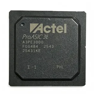
A3PE1500-2FG484 - ProASIC3E FPGA, 1.5M Gates | Microchip
部品番号: A3PE1500-2FG484 ✓ 生産中| 数量 | 単価 | 小計 |
|---|---|---|
| 1 | $290.66 | $290.66 |
| 10 | $275 | $2,750.00 |
| 100 | $250 | $25,000.00 |
| 500 | $230 | $115,000.00 |
| 1,000 | $210 | $210,000.00 |
A3PE1500-2FG484 概要
A Field Programmable Gate Array (FPGA) is an integrated circuit that can be configured by the customer after manufacturing. Unlike fixed-function ASICs, FPGAs contain an array of programmable logic blocks and interconnects that can be programmed to implement any digital logic function. The ProASIC3E family uses flash-based configuration cells, which retain the program even when power is removed, providing instant-on operation and inherent security against reverse engineering. This makes them suitable for applications requiring secure boot and tamper resistance.
Key features of the A3PE1500-2FG484 include 1.5 million system gates, 280 user I/Os, and 276,480 bits of RAM. It supports up to 16K logic elements (LEs) and includes advanced features such as phase-locked loops (PLLs), SRAM/FIFO, and programmable I/O standards. The flash-based architecture eliminates the need for external configuration memory, reducing system cost and board space. The device also offers low power consumption, with a typical static power of 0.11W, making it ideal for power-sensitive applications.
Technically, the ProASIC3E core tile is a VersaTile that can be configured as a three-input lookup table (LUT) or as a D-flip-flop/latch with enable. This flexibility allows efficient use of the FPGA fabric. The device includes up to 6 PLLs, which can be used for clock generation and synchronization. The I/O supports various standards including LVCMOS, LVTTL, PCI, and LVDS, providing interface flexibility. The flash-based configuration also provides immunity to single-event upsets (SEU) in radiation environments, making it suitable for aerospace and defense applications.
Typical applications for the A3PE1500-2FG484 include industrial automation, communications infrastructure, medical imaging, and aerospace systems. Its low power and instant-on capability make it suitable for battery-powered portable devices. The 280 I/Os allow interfacing with multiple peripherals, and the embedded RAM can be used for data buffering and FIFO implementation.
When designing with this FPGA, consider the 1.5V core supply and the need for proper decoupling. The device requires multiple power rails (VCC, VCCPLL, VCCIBx) and careful PCB layout to minimize noise. Use the Microchip Libero SoC design suite for programming and configuration. The flash-based nature allows in-system programming, simplifying field updates.
This page synthesizes distributor pricing, drop-in alternatives, and practical design notes not found in the manufacturer datasheet, providing a comprehensive resource for engineers evaluating the A3PE1500-2FG484.
ドロップイン代替品: A3PE1500-2FG484 — 同一パッケージでピン互換。PCBの作り直しが必要な異なるパッケージの部品は除外されています。
このシリーズのバリエーション
同一シリーズでドロップイン互換のモデル: A3PE1500-2FG484 (同一形状・フットプリント) — 相違点: Configuration Memory, Package, Process Technology, System Gates, Speed Grade.
クイック比較ツール — 並列比較する代替部品を選択:
A3PE1500-2FGG484
✅ ドロップイン📋 参考代替品(カタログ未掲載)
A3PE1500-2FG484I
✅ ドロップイン📋 参考代替品(カタログ未掲載)
A3PE1500-2FGG484I
✅ ドロップイン✓ 在庫あり
$195 / 個
データシートを見る →A3PE1500-FGG484I
✅ ドロップイン📋 参考代替品(カタログ未掲載)
A3PE1500-1FG484
✅ ドロップイン✓ 在庫あり
$74.2 / 個
データシートを見る →A3PE1500-1FGG484
✅ ドロップイン✓ 在庫あり
$48.1 / 個
データシートを見る →A3PE1500-2FG484 最大定格&電気的特性
| Family | ProASIC3E |
| System Gates | 1,500,000 |
| Logic Elements (LEs) | 16K |
| User I/Os | 280 |
| RAM Bits | 276,480 |
| Core Supply Voltage | 1.5V |
| I/O Supply Voltage | 1.5V to 3.3V |
| パッケージ | 484-FBGA |
| 動作温度 | 0°C to 70°C |
| Number of PLLs | 6 |
| Configuration | Flash-based |
| 実装タイプ | Surface Mount |
| RoHS ステータス | Compliant |
| Speed Grade | -2 |
| Total Power (Typical) | 0.11W static |
A3PE1500-2FG484 484-fbga ピン配置ガイド
A3PE1500-2FG484 (484-fbga パッケージ) のピン配置。 このデジタルICには、GPIO、通信インターフェース (UART、SPI、I2C)、および電源ピンが含まれています。代替ピン機能と設定オプションについては、メーカーのデータシートを参照してください。組み込みシステム設計とPCBレイアウトに不可欠です。

詳細なピン配置データはありません: A3PE1500-2FG484.
詳細は データシート をご参照ください。
主な用途
A3PE1500-2FG484 の用途: 6 件s: Industrial Automation, Communications Infrastructure, Medical Imaging, Aerospace and Defense, Portable Electronics, Data Acquisition and Control.
Industrial Automation
The A3PE1500-2FG484 is ideal for industrial automation due to its low power consumption (0.11W static) and instant-on capability, which is critical for safety systems that must start immediately. With 280 user I/Os, it can interface with multiple sensors, actuators, and communication interfaces. The flash-based configuration ensures secure and reliable operation in harsh environments. Its 1.5V core supply reduces power dissipation, making it suitable for compact industrial controllers. The device's 276,480 RAM bits can be used for data buffering in real-time control loops. Additionally, the 6 PLLs provide flexible clocking for motor control and data acquisition. The ProASIC3E family's radiation tolerance makes it suitable for industrial environments with electromagnetic interference. Overall, the A3PE1500-2FG484 offers a balance of performance, power, and reliability for industrial applications.
おすすめ
Communications Infrastructure
In communications infrastructure, the A3PE1500-2FG484 excels due to its high I/O count (280) and support for various I/O standards including LVCMOS, LVTTL, PCI, and LVDS. This allows direct interfacing with network processors, PHYs, and backplane transceivers. The 6 PLLs enable precise clock generation for synchronous data transmission. The flash-based configuration provides instant-on, reducing system boot time in network equipment. The device's low power consumption is beneficial for line cards where thermal management is critical. The 276,480 RAM bits can be used for packet buffering and FIFO implementation. The ProASIC3E family's security features protect intellectual property in communication systems. With 1.5M gates, it can handle protocol bridging, framing, and error correction. The 484-FBGA package offers a compact footprint for dense PCB layouts. Overall, the A3PE1500-2FG484 is a reliable choice for communication equipment requiring flexibility and low power.
おすすめ
Medical Imaging
The A3PE1500-2FG484 is well-suited for medical imaging systems such as ultrasound and MRI, where low noise and high reliability are paramount. Its flash-based architecture provides inherent immunity to configuration upsets, ensuring stable operation. The 280 I/Os allow interfacing with high-speed ADCs and DACs, while the 276,480 RAM bits can buffer image data. The 6 PLLs generate precise clocks for sensor synchronization. The device's low power consumption reduces heat generation, which is critical in enclosed medical devices. The commercial temperature range (0°C to 70°C) is suitable for most medical equipment. The ProASIC3E family's security features protect patient data and device firmware. With 1.5M gates, it can implement image processing algorithms such as filtering and edge detection. The 484-FBGA package enables compact PCB designs. Overall, the A3PE1500-2FG484 offers the performance and reliability needed for medical imaging applications.
おすすめ
Aerospace and Defense
The A3PE1500-2FG484 is designed for aerospace and defense applications due to its flash-based configuration, which provides immunity to single-event upsets (SEU) and secure boot. The device operates from 0°C to 70°C, but the industrial grade (-2FG484I) is available for wider temperature ranges. The 280 I/Os support various protocols including LVDS for high-speed data links. The 6 PLLs enable precise clocking for radar and communication systems. The low power consumption (0.11W static) is critical for battery-powered and space-constrained systems. The 276,480 RAM bits can be used for telemetry data buffering. The ProASIC3E family's security features prevent reverse engineering of military algorithms. With 1.5M gates, it can implement complex signal processing and control logic. The 484-FBGA package is rugged and suitable for harsh environments. Overall, the A3PE1500-2FG484 is a trusted choice for defense electronics.
おすすめ
Portable Electronics
The A3PE1500-2FG484 is ideal for portable electronics due to its low power consumption (0.11W static) and instant-on capability, which extends battery life and provides immediate response. The 1.5V core supply reduces power dissipation. The 280 I/Os allow interfacing with displays, sensors, and wireless modules. The 276,480 RAM bits can be used for data buffering in audio or image processing. The 6 PLLs generate clocks for various peripherals. The flash-based configuration eliminates the need for external configuration memory, saving board space and cost. The commercial temperature range is suitable for consumer devices. The 484-FBGA package is compact, enabling slim designs. With 1.5M gates, it can handle user interface logic, protocol handling, and data processing. The device's security features protect firmware from unauthorized access. Overall, the A3PE1500-2FG484 offers a balance of performance and power efficiency for portable applications.
おすすめ
Data Acquisition and Control
The A3PE1500-2FG484 is well-suited for data acquisition and control systems, offering 280 user I/Os to interface with multiple sensors and actuators. The 276,480 RAM bits provide ample buffering for high-speed data streams. The 6 PLLs enable precise sampling clocks for ADCs and DACs. The flash-based configuration ensures reliable operation in industrial environments. The device's low power consumption reduces heat in control cabinets. The 1.5V core supply is compatible with modern low-voltage logic. The ProASIC3E family's security features protect control algorithms. With 1.5M gates, it can implement PID controllers, data logging, and communication protocols. The 484-FBGA package allows for compact PCB layouts. The commercial temperature range is suitable for most industrial settings. Overall, the A3PE1500-2FG484 provides a flexible and reliable platform for data acquisition and control applications.
おすすめ
おすすめ製品の概要
エンジニアリング参考データ: A3PE1500-2FG484 — 比較、設計ガイダンス、コンプライアンス情報。
選定ガイド
代替品との比較
| パラメータ | この製品 | A3PE1500-2FGG484 | A3PE1500-2FG484I | A3PE1500-2FGG484I | A3PE1500-FGG484I | A3PE1500-1FG484 | A3PE1500-1FGG484 |
|---|---|---|---|---|---|---|---|
| Package | 484-FBGA | 484-FBGA | 484-FBGA | 484-FBGA | 484-FBGA | 484-FBGA | 484-FBGA |
| Brand | Microchip Technology | Microchip Technology | Microchip Technology | Microchip Technology | Microchip Technology | Microchip Technology | Microchip Technology |
| System Gates | 1,500,000 | 1,500,000 | 1,500,000 | 1,500,000 | 1,500,000 | 1,500,000 | 1,500,000 |
| User I/Os | 280 | 280 | 280 | 280 | 280 | 280 | 280 |
| RAM Bits | 276,480 | 276,480 | 276,480 | 276,480 | 276,480 | 276,480 | 276,480 |
| Speed Grade | -2 | -2 | -2 | -2 | -1 | -1 | -1 |
| Operating Temperature | 0°C to 70°C | 0°C to 70°C | -40°C to 100°C | -40°C to 100°C | -40°C to 100°C | 0°C to 70°C | 0°C to 70°C |
| RoHS Compliant | Yes | Yes | Yes | Yes | Yes | Yes | Yes |
主な差別化要因
- Flash-based configuration with instant-on and security (vs SRAM-based FPGAs (e.g., Xilinx Spartan-6))
- Low static power consumption (0.11W) (vs A3PE3000-2FG484I)
- 280 user I/Os in a 484-FBGA package (vs A3PE1500-2PQG208I)
設計ノート
The A3PE1500-2FG484 requires a 1.5V core supply (VCC) and separate I/O supplies (VCCIBx) that can range from 1.5V to 3.3V. Use low-ESR ceramic capacitors (0.1uF and 10uF) placed close to each power pin to decouple high-frequency noise. The typical static power is 0.11W, but dynamic power depends on logic activity and clock frequency. Estimate total power using the Microchip power calculator to ensure adequate thermal management.
For the 484-FBGA package, use a multi-layer PCB with dedicated power and ground planes. Route high-speed I/O signals with controlled impedance (e.g., 50 ohm for single-ended, 100 ohm differential for LVDS). Place decoupling capacitors on the bottom side directly under the BGA pads to minimize inductance. Follow the layout guidelines in the ProASIC3E datasheet (DS0098) for optimal signal integrity.
The A3PE1500-2FG484 has a maximum junction temperature of 125°C. With a typical static power of 0.11W, thermal management is usually not critical, but dynamic power can increase significantly. Use a thermal via array under the BGA to conduct heat to the ground plane. For high-activity designs, consider adding a heatsink or forced airflow. Estimate junction temperature using theta_JA from the datasheet and the total power dissipation.
コンプライアンス情報
RoHS compliant per distributor listings. Not AEC-Q100 qualified. Lead-free finish on FGG variants.