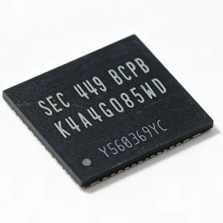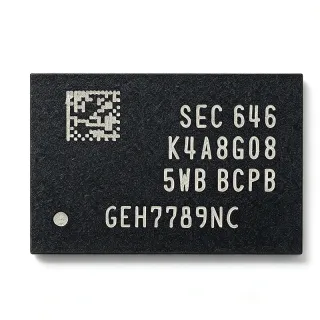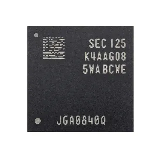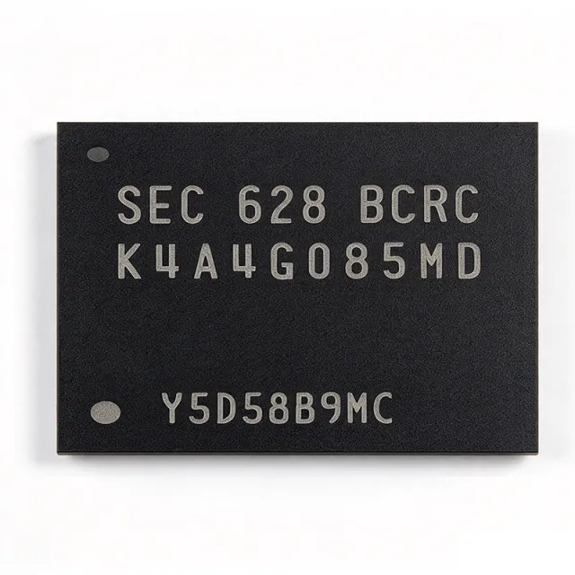
K4A4G085WD-BCRC - 4Gb DDR4-2400 SDRAM 512Mx8 | Samsung
部品番号: K4A4G085WD-BCRC ✓ 生産中| 数量 | 単価 | 小計 |
|---|---|---|
| 1 | $7.0313 | $7.03 |
| 10 | $5.0781 | $50.78 |
| 100 | $4.4922 | $449.22 |
| 500 | $4.2969 | $2,148.45 |
| 1,000 | $4.1016 | $4,101.60 |
K4A4G085WD-BCRC 概要
DDR4 SDRAM is the fourth generation of Double Data Rate synchronous dynamic random-access memory, a class of volatile memory ICs that transfer data on both clock edges. Within the memory hierarchy, DDR4 sits above DDR3 and below DDR5, and is the dominant DRAM technology for embedded controllers, industrial modules, and enterprise computing platforms. Compared to DDR3, DDR4 lowers the core supply from 1.5V to 1.2V, raises bank-group parallelism, and improves bus speeds.
Key features of the K4A4G085WD-BCRC include the 4Gbit density in a byte-wide x8 organization, DDR4-2400 speed grade (BCRC speed bin), and 1.2V low-voltage operation that reduces system power versus DDR3. The device supports standard DDR4 features such as bank-group architecture, on-die termination (ODT), and DBI/CRC functionality typical of the DDR4 specification.
Technically, the D-die Samsung DDR4 family uses a scaled DRAM process with bank groups enabling higher effective bandwidth. The x8 organization suits designs using a single chip per data lane, simplifying layout for microcontroller FMC/SDRAM-style controllers and industrial compute modules that need moderate bandwidth and non-standard memory sizing.
Typical applications include industrial controllers and PLCs requiring DRAM working memory, embedded computing and networking modules, firmware logging and data buffering systems, and replacement sourcing for legacy DDR4-based BOM lines. Distributors such as Jotrin, Censtry, and Weyland list the part as DDR4 512Mx8 PC2400.
Design consideration: DDR4 demands careful signal-integrity work - length-matched fly-by routing of CK/CA/DQS, accurate VTT termination on the 1.2V bus, and controller configuration of tRFC and ZQ calibration. Verify the exact speed bin suffix (BCRC) against your controller's supported rates.
This page synthesizes distributor pricing, drop-in alternatives across Samsung die generations and a JEDEC-compatible Micron equivalent, plus practical DDR4 design notes not found in the manufacturer datasheet.
ドロップイン代替品: K4A4G085WD-BCRC — 同一パッケージでピン互換。PCBの作り直しが必要な異なるパッケージの部品は除外されています。
クイック比較ツール — 並列比較する代替部品を選択:
K4A4G085WE-BCRC
✓ 在庫あり
$1.36 / 個
データシートを見る →K4A4G085WD-BCPB
✓ 在庫あり
価格はお問い合わせください
データシートを見る →K4A4G085WD
✓ 在庫あり
$2.05 / 個
データシートを見る →MT40A512M8RH-075E:B
✓ 在庫あり
$2.15 / 個
データシートを見る →K4A4G085WB-BCRC
📋 参考代替品(カタログ未掲載)
K4A4G085WD-BCRC 最大定格&電気的特性
| メモリタイプ | DDR4 SDRAM |
| Density | 4 Gbit |
| メモリ構成 | 512M x 8 |
| Speed Grade | DDR4-2400 (PC4-2400) |
| 電源電圧 | 1.2 V |
| Die Generation | D-die |
| パッケージ | 78-ball FBGA |
| 実装タイプ | Surface Mount |
| インターフェース | Parallel (DDR4) |
| Bank Groups | Yes (DDR4 architecture) |
| On-Die Termination (ODT) | Yes |
| Refresh | Standard DDR4 refresh (8K/64ms nominal) |
| RoHS ステータス | Compliant |
| Manufacturers Part Number Full | K4A4G085WD-BCRC |
K4A4G085WD-BCRC 78-ball fbga ピン配置ガイド
K4A4G085WD-BCRC (78-ball fbga パッケージ) のピン配置。 このデジタルICには、GPIO、通信インターフェース (UART、SPI、I2C)、および電源ピンが含まれています。代替ピン機能と設定オプションについては、メーカーのデータシートを参照してください。組み込みシステム設計とPCBレイアウトに不可欠です。

詳細なピン配置データはありません: K4A4G085WD-BCRC.
詳細は データシート をご参照ください。
主な用途
K4A4G085WD-BCRC の用途: 6 件s: Industrial Controllers and PLCs, Embedded Computing Modules, Firmware Boot and Data Logging, Network Appliances and Routers, Test and Measurement Instruments, Legacy DDR4 BOM Replacement Sourcing.
Industrial Controllers and PLCs
The K4A4G085WD-BCRC provides 4Gb of DDR4 working memory at DDR4-2400 with 1.2V operation, matching the memory demands of industrial controllers running RTOS firmware, motion-control loops, and data logging. Its 512M x 8 organization fits single-device-per-lane controller buses common in PLC CPU modules, and GlobalSpec explicitly lists industrial controllers as a target use. The DDR4-2400 speed class delivers sufficient bandwidth for control loops and HMI buffering, while standard DDR4 features such as ODT and bank groups simplify controller bring-up. Place the device close to the SoC with fly-by CA routing and solid 1.2V and VTT planes; industrial ambient temperatures require confirming the bin's rated operating range.
おすすめ
Embedded Computing Modules
Embedded computing and networking modules use the K4A4G085WD-BCRC as main system DRAM: 4Gb in a single 78-ball FBGA gives compact boards enough memory for Linux-class workloads without a multi-chip DDR4 array. The 1.2V rail integrates cleanly with modern SoC power trees, and the DDR4-2400 rate matches mainstream ARM and x86 embedded SoC memory controllers. Because the x8 FBGA-78 ballout is JEDEC-standard, module designers can dual-source with Micron MT40A512M8RH-075E:B or alternate Samsung die generations (WE, WB) with minimal requalification. Design the module with length-matched byte lanes and per-device ZQ resistors; module-level thermal spreading under the FBGA keeps DRAM refresh margins stable at sustained bandwidth.
おすすめ
Firmware Boot and Data Logging
For embedded logging, firmware boot buffering, and runtime data capture, the K4A4G085WD-BCRC supplies 512MB of fast volatile buffer memory that pairs with serial NAND or eMMC boot storage. Samsung's own K9-series NAND devices (for example K9DUGY8S7M) complement the DDR4: code boots from flash into DRAM, then logs stream through the 4Gb buffer at DDR4-2400 rates. The x8 organization maps directly onto 8-bit logging buses and simplifies ECC layout. Because logging systems run continuously, monitor DRAM temperature and leverage the standard DDR4 refresh scheme (8K refresh nominal over 64ms); the 1.2V core keeps continuous-operation power low compared with DDR3 alternatives at equal density.
おすすめ
Network Appliances and Routers
Networking equipment such as routers, switches, and gateways relies on DRAM for packet buffering, routing tables, and management-plane software. The K4A4G085WD-BCRC's DDR4-2400 interface provides the sustained bandwidth needed for line-rate packet forwarding in mid-range appliances, while 4Gb capacity comfortably hosts Linux-based management stacks. The 78-ball FBGA footprint allows two devices to populate a 64-bit plus ECC controller bus, a common topology in network silicon reference designs. Because networking hardware runs 24/7 in controlled cabinets, the 1.2V rail and low-refresh overhead translate to meaningful fleet-level energy savings versus DDR3 designs; verify CAS latency settings against the BCRC timing table for worst-case temperature.
おすすめ
Test and Measurement Instruments
Oscilloscope, data-acquisition, and signal-analyzer front ends capture high-rate sample streams that must be buffered into DRAM before processing. The K4A4G085WD-BCRC's DDR4-2400 byte-wide interface sustains the streaming throughput needed between ADC/FPGA capture logic and processor memory, and 4Gb per device allows deep capture memory when ganged across a 64-bit controller bus. Samsung D-die DDR4 in the JEDEC-standard FBGA-78 footprint lets instrument designers pre-qualify a layout once and then source from Samsung WB/WD/WE generations or Micron equivalents. Layout priority: keep DQS-to-DQ trace skew within DDR4 spec, use solid reference planes under the byte lanes, and provision the 1.2V rail with low-ESR bulk plus high-frequency ceramic decoupling.
おすすめ
Legacy DDR4 BOM Replacement Sourcing
Many fielded products were built around 4Gb x8 DDR4 and now face end-of-life sourcing gaps. The K4A4G085WD-BCRC, and its drop-in peers K4A4G085WE-BCRC and K4A4G085WB-BCRC, let buyers re-populate legacy BOM lines without PCB changes because all use the JEDEC-standard 78-ball x8 DDR4 footprint. Replacement sourcing teams should compare speed-bin suffixes (BCRC, BCTD, BCWE), confirm the memory controller timing table covers the substitute bin, and prefer the newest die generation (E-die) for longest future availability. Distributors such as Censtry and Weyland stock the BCRC specifically for replacement demand, with 180-day warranties and test reports available on request for quality assurance.
おすすめ
おすすめ製品の概要
エンジニアリング参考データ: K4A4G085WD-BCRC — 比較、設計ガイダンス、コンプライアンス情報。
選定ガイド
代替品との比較
| パラメータ | この製品 | K4A4G085WE-BCRC | K4A4G085WD-BCPB | K4A4G085WB-BCRC | MT40A512M8RH-075E |
|---|---|---|---|---|---|
| Package | 78-ball FBGA | 78-ball FBGA - same | 78-ball FBGA - same footprint, package option code differs | 78-ball FBGA - same | B: 78-ball FBGA (JEDEC x8) - same |
| Brand | Samsung Electronics | Samsung Electronics | Samsung Electronics | Samsung Electronics | B: Micron Technology |
| Density | 4 Gbit | 4 Gbit | 4 Gbit | 4 Gbit | B: 4 Gbit |
| Organization | 512M x 8 | 512M x 8 | 512M x 8 | 512M x 8 | B: 512M x 8 |
| Supply Voltage | 1.2 V | 1.2 V | 1.2 V | 1.2 V | B: 1.2 V |
| Die Generation | D-die | E-die (newer) | D-die | B-die (older) | B: Micron 8Gb-class monolithic die |
| Lifecycle Status | Active | Active (newest die, longest life expected) | Active | Active (older die, shorter expected life) | B: Active |
主な差別化要因
- Current D-die generation with long sourcing runway (vs K4A4G085WB-BCRC)
- Same speed code, newer die option exists (vs K4A4G085WE-BCRC)
- JEDEC-standard x8 footprint enables true cross-brand drop-in (vs MT40A512M8RH-075E:B)
設計ノート
DDR4-2400 fly-by topology is mandatory for CK/CA/address signals: route them in a daisy chain from controller through each DRAM with 40-ohm controlled impedance and VTT termination (0.6V) at the chain end. DQ/DQS/DM byte lanes must be length-matched within the DDR4 spec skew budget, referencing a continuous ground plane. With the FBGA-78 package, keep the ZQ calibration resistor (240 ohm 1%) within a few millimeters of the ZQ ball with no stubs.
Budget three rails: VDD/VDDQ at 1.2V, VPP at 2.5V, and VTT at 0.6V (VDDQ/2) for termination. Estimated: at DDR4-2400 a single 4Gb x8 device typically draws a few hundred milliamps peak from the 1.2V rail - size the VTT source/sink LDO for termination current that can be bidirectional and substantial in write bursts. Use bulk capacitance near each device plus per-ball high-frequency ceramics; VTT must track VDDQ/2 within tolerance under transient load.
Do not mix die generations (B/WD/E) on the same byte-lane bus without requalifying the timing table - tRFC and output slew differ between Samsung generations, and controller training must be rerun. Also verify the speed suffix when purchasing: BCRC, BCTD, and BCWE denote different speed bins even within the same K4A4G085WD family; ordering the wrong bin can cause marginal timing at 2400 MT/s. Finally, confirm the E-die substitution (K4A4G085WE-BCRC) supports your controller's DDR4 initialization sequence before mass production.
コンプライアンス情報
RoHS compliance per standard Samsung DDR4 production policy; formal REACH/halogen-free/conflict-minerals declarations should be requested from Samsung environmental documentation for the specific date code.