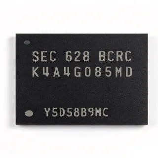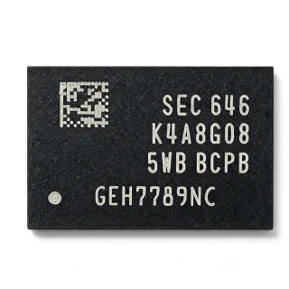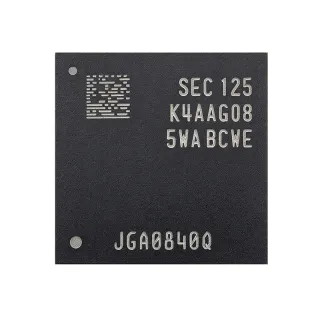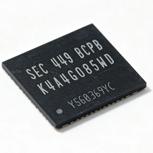
K4A4G085WD - 4Gb DDR4 SDRAM 512Mx8 BGA | Samsung
MPN: K4A4G085WD ✓ Active| Qty | Unit Price | Extended |
|---|---|---|
| 1 | $3.2 | $3.20 |
| 10 | $2.95 | $29.50 |
| 100 | $2.6 | $260.00 |
| 500 | $2.3 | $1,150.00 |
| 1,000 | $2.05 | $2,050.00 |
K4A4G085WD Overview
A DDR4 SDRAM (Double Data Rate 4 Synchronous Dynamic Random Access Memory) is a type of volatile DRAM that transfers data on both clock edges, doubling effective bandwidth versus SDR memory. Within the memory hierarchy it sits as the main-system-memory tier: DRAM cell -> DDR SDRAM -> DDR4 SDRAM -> memory IC -> semiconductor memory. DDR4 introduced the bank-group architecture, lower 1.2V operation, and improved on-die termination (ODT) relative to DDR3.
Key features of the K4A4G085WD include the 8-bit-wide x8 I/O organization with 512M addressable locations, the DDR4 bank-group architecture that accelerates random access by permitting interleaved access to different bank groups, and low 1.2V power operation that cuts power consumption versus DDR3. Built-in termination and the CA parity option improve signal integrity at high bus speeds on long, heavily loaded memory buses.
The D-die core uses Samsung's scaled DRAM cell technology, supporting standard DDR4 timing parameters such as tRCD, tRP and tRAS per the JEDEC DDR4 specification framework and the Samsung product guide. The 78-ball FBGA (Fine-Pitch Ball Grid Array, lead-free solder balls) keeps the footprint compact for dense memory subsystems, and the part is available in commercial speed grades such as -BCPB (DDR4-2400) and -BCRC, as identified in the Samsung DDR4 SDRAM Memory product guide (May 2018).
Typical applications include embedded controllers, industrial computing modules, networking equipment, set-top boxes, and replacement/repair sourcing for PC DIMMs and UDIMM/SODIMM assemblies using x8 DRAM components.
When designing with this device, follow Samsung's layout guidance for fly-by command/address routing, per-byte DQS strobe matching, and 40-ohm ODT calibration; address-bus integrity at DDR4-2400 is the most common failure point in first-turn boards.
This page synthesizes verified datasheet data, drop-in alternatives across Samsung, Micron and SK Hynix families, practical design notes, and procurement information not found in the manufacturer datasheet alone.
Drop-in alternatives for K4A4G085WD — same package, pin-to-pin compatible. Different-package parts requiring PCB rework are excluded.
Variants in this series
Same-series models that are drop-in compatible with K4A4G085WD (same form factor and footprint) — differing in Package, Memory Type, Mounting Type, Data Rate, Interface.
Quick Comparison Tool — Select alternative parts for side-by-side comparison:
K4A4G085WD-BCRC
✓ In Stock
$3.58 / Unit
View Datasheet →K4A4G085WD-BCPB
✓ In Stock
Contact for price
View Datasheet →K4A4G045WD-BCPB
✓ In Stock
$2.2 / Unit
View Datasheet →MT40A512M8RH-075E:B
✓ In Stock
$2.15 / Unit
View Datasheet →H5AN4G8NMFAR
📋 Reference alternative (not in catalog)
K4A4G085WD Maximum Ratings & Electrical Characteristics
| Memory Type | DDR4 SDRAM |
| Die Generation | D-die |
| Density | 4 Gb |
| Organization | 512M x 8 |
| Data Rate | Up to 2400 Mbps (speed-grade dependent) |
| Supply Voltage (VDD) | 1.2 V |
| Package | 78-ball FBGA |
| Mounting Type | Surface Mount |
| Speed Grade (example) | -BCPB (DDR4-2400), -BCRC |
| Interface Type | DDR4 (double data rate, source-synchronous) |
| Bank Group Architecture | Yes (DDR4 bank groups) |
| ODT | On-Die Termination (built-in) |
K4A4G085WD 78-ball fbga Pin Configuration Guide
Pin configuration for K4A4G085WD (78-ball fbga package). This digital IC includes GPIO, communication interfaces (UART, SPI, I2C), and power pins. Refer to the manufacturer datasheet for alternate pin functions and configuration options. Essential for embedded system design and PCB layout.

No detailed pinout data available for K4A4G085WD.
Refer to the datasheet for full pin configuration.
Typical Applications
K4A4G085WD is suitable for 6 applications: Embedded Industrial Controllers, Computing Modules and SBCs, Networking and Communication Equipment, PC DIMM / Memory Module Replacement Sourcing, Video and Display Processing Systems, Data Logging and Firmware Boot Systems.
Embedded Industrial Controllers
Industrial controllers and PLC-class CPUs require dense, reliable main memory, and the K4A4G085WD's 4Gb 512M x 8 DDR4 organization with 1.2V operation fits that role directly. Distributor product descriptions explicitly position the K4A4G085WD-BCRC family for industrial controllers and embedded logging. In this use, the DRAM connects to the processor's DDR4 controller in a fly-by command/address topology with built-in on-die termination (ODT) handling bus loading at DDR4-2400-class speeds. The x8 width lets designers build 64-bit buses with ECC using eight devices. The compact 78-ball FBGA saves board area versus older DDR3 footprints while the bank-group architecture improves effective bandwidth for logging and control-loop workloads. Expect power savings versus DDR3 thanks to the reduced 1.2V rail.
Recommended
Computing Modules and SBCs
Single-board computers and SOM (system-on-module) designs need mainstream DRAM with wide sourcing, and the K4A4G085WD is a mainstream 4Gb x8 DDR4 part cross-referenced across Samsung, Micron and SK Hynix families. In a computing module, four to eight of these x8 devices populate a 32- or 64-bit DDR4 bus, with source-synchronous DQS strobes matched per byte lane. The device's bank-group architecture sustains the random-access throughput that Linux-class SoCs demand, and its 1.2V operation keeps module power budgets tight. Because DDR4 FBGA ballouts are standardized, a layout designed around the K4A4G085WD can typically second-source to Micron MT40A512M8 or Hynix H5AN4G8 parts with minimal requalification, reducing supply risk for long-life module products.
Recommended
Networking and Communication Equipment
Routers, switches and carrier-grade networking line cards use x8 DDR4 SDRAM for packet buffering, route tables and control-plane memory. The K4A4G085WD's DDR4 bank-group structure is specifically valuable here: it allows simultaneous open pages in different bank groups, boosting random-access efficiency for bursty packet I/O patterns. Its 1.2V VDD reduces power per bit, important in fanless network appliances, and the built-in ODT eases signal integrity on the heavily loaded multi-drop address bus typical of 4-8 chip memory subsystems. At DDR4-2400-class rates, one x8 device supplies up to 2.4 GB/s of peak bandwidth, so a 64-bit bank of eight devices provides over 19 GB/s aggregate - sufficient for mid-range switch control planes and network-attached storage buffers.
Recommended
PC DIMM / Memory Module Replacement Sourcing
The K4A4G085WD is a component-level part used in UDIMM, SODIMM and RDMM DDR4 module builds, making it a natural choice for module repair, remanufacturing and replacement sourcing. A standard unbuffered DDR4 DIMM uses eight to sixteen x8 DRAMs exactly like this one per 64-bit rank. Distributor listings highlight replacement sourcing as a primary use case for the K4A4G085WD-BCRC family. When repairing or rebuilding modules, match the speed suffix and refresh binning to the original SPD data so the module's programmed timings remain valid, and verify date-code consistency across the eight or sixteen devices on a rank, since mixed-bin devices can cause intermittent training failures during memory initialization at DDR4-2400-class speeds.
Recommended
Video and Display Processing Systems
Video processors, set-top boxes and digital signage platforms need cost-effective frame-buffer memory, and 4Gb DDR4 provides roughly 512 MB per device - ample for multi-frame 1080p/4K buffering. The K4A4G085WD sustains DDR4-2400-class transfers, delivering the deterministic bandwidth needed for display refresh plus decode pipelines when several x8 devices form a wide bus. Its bank-group architecture helps video engines that read and write different frame regions concurrently, reducing effective row-miss penalties versus single-bank DDR3 designs. The low 1.2V rail simplifies power design in sealed, fanless signage hardware. Designers should budget bus bandwidth between display scan-out and decode engines, and use ODT settings per Samsung's DDR4 design guide to keep eye diagrams clean on longer traces.
Recommended
Data Logging and Firmware Boot Systems
Distributor product data lists embedded logging and firmware boot among the primary applications of the K4A4G085WD-BCRC family. In data loggers, the DRAM acts as a high-speed write buffer between sensors/communication interfaces and slower nonvolatile storage, absorbing burst data at DDR4 speeds before bulk flushing to flash. For boot systems, DRAM is the execution workspace that bootloaders relocate code into after ROM initialization. The K4A4G085WD's 4Gb capacity supports memory-resident analytics on logged data, and its 1.2V operation suits battery-backed and energy-harvesting loggers. Memory-controller training at power-up is the key integration step - ensure your bootloader supports DDR4 leveling (read/write leveling, DQS drift compensation) for robust cold-start behavior across temperature extremes.
Recommended
Recommended Products Summary
Engineering reference data for K4A4G085WD — comparison, design guidance, and compliance information.
Selection Guide
Comparison with Alternatives
| Parameter | This Product | K4A4G085WD-BCRC | MT40A512M8RH-075E | H5AN4G8NMFAR |
|---|---|---|---|---|
| Package | 78-ball FBGA | 78-ball FBGA - same | B: 78-ball FBGA - same | 78-ball FBGA - same |
| Brand | Samsung Electronics | Samsung Electronics | B: Micron Technology | SK Hynix |
| Density | 4 Gb | 4 Gb | B: 4 Gb | 4 Gb |
| Organization | 512M x 8 | 512M x 8 | B: 512M x 8 | 512M x 8 |
| Memory Interface | DDR4 | DDR4 | B: DDR4 | DDR4 |
| Supply Voltage | 1.2 V | 1.2 V | B: 1.2 V | 1.2 V |
| Die Generation / Source | Samsung D-die | Samsung D-die (same) | B: Micron die | SK Hynix die |
Key Differentiators
- Samsung D-die mainstream process with wide second-source ecosystem (vs MT40A512M8RH-075E:B)
- Identical die family across speed grades enables flexible binning (vs K4A4G045WD-BCPB)
- DDR4 bank-group architecture for random-access efficiency (vs H5AN4G8NMFAR)
Design Notes
DDR4 controllers use fly-by routing for command/address/clock: daisy-chain CA signals through each DRAM in the rank, terminating at the far end. Keep clock-to-CA skew tight and match each DQS strobe to its data byte lane within the controller's specified window. Per-device trace-length matching to the clock must follow your processor's memory design guide. Place the 1.2V VDD decoupling network (multiple 100 nF ceramics plus bulk capacitance per device) close to each FBGA, since DDR4 transient currents are sharp and rail droop directly degrades write margins.
On-die termination (ODT) values must be programmed to match your topology - for a two-rank bus the termination on the idle rank heavily influences the far-end eye. Use the processor's ODT and drive-strength table, then verify with read/write eye measurements at DDR4-2400 on first-turn boards. The most common first-silicon failure is a marginal address bus at full speed; if your controller supports it, reduce the initial speed grade during bring-up and step up after confirming leveling results across all ranks and temperatures.
Estimated: a 4Gb DDR4 x8 device at DDR4-2400 draws on the order of a few hundred milliwatts active (background + access power per JEDEC-class current figures), so an eight-device 64-bit bank is a load in the 1-3 W range active - size the 1.2V buck converter and its thermal budget accordingly, and budget VPP (2.5V) per the datasheet. Disable unused ranks via CKE to cut standby power. Confirm exact IDD currents for your speed grade and temperature bin in the Samsung datasheet before finalizing the power tree.
Do not mix speed-grade suffixes (e.g., -BCPB with -BCRC) within one rank: mixed binning can pass POST but fail intermittently at temperature extremes because refresh and timing margins differ. Always verify the complete ordering part number suffix when procuring, since the bare base MPN does not fully define speed, temperature, or refresh binning. Cross-brand substitution (Samsung to Micron or SK Hynix) requires re-running memory-controller training and revalidating SPD data in module applications.
Compliance Information
Verified web data for this page did not include explicit compliance statements; Samsung product pages list RoHS/REACH status per ordering part number. Confirm on the Samsung product page for the exact suffix before use.