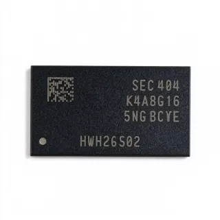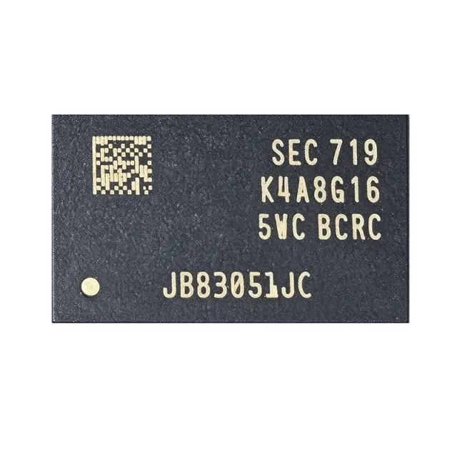
K4A8G165WC-BCRC - 8Gb DDR4 SDRAM 2400Mbps x16 | Samsung
部品番号: K4A8G165WC-BCRC ✓ 生産中| 数量 | 単価 | 小計 |
|---|---|---|
| 1 | $33.75 | $33.75 |
| 10 | $24.375 | $243.75 |
| 100 | $21.5625 | $2,156.25 |
| 500 | $20.625 | $10,312.50 |
| 1,000 | $19.6875 | $19,687.50 |
K4A8G165WC-BCRC 概要
DDR4 SDRAM (Double Data Rate 4 Synchronous Dynamic Random Access Memory) is the fourth generation of the JEDEC-defined DDR memory family. In the system hierarchy it sits under synchronous DRAM -> volatile memory IC -> semiconductor memory, serving as the main working memory for processors, SoCs and controllers. DDR4 lowered operating voltage from DDR3's 1.5 V to 1.2 V, cutting dynamic power by roughly 25% while raising data rates up to 3200 Mbps.
Key features of this C-die part include an 8 Gbit density in a x16 organization with a 16-bit data interface, auto precharge, asynchronous reset, CRC and CA parity for command/address integrity, on-die ZQ calibration, dynamic on-die termination (ODT), and data mask (DM) support per byte lane. These features improve signal integrity and data reliability at high speeds.
Technically, the device uses Samsung's C-die process and a bank-group architecture that allows faster burst access between bank groups. Ballouted per JEDEC DDR4 standards, the 96-ball FBGA is the industry-standard footprint, so JEDEC-compliant x16 8 Gb DDR4 parts from other vendors land on the same PCB land pattern. Operating current is specified around 2 mA (standby idle) and up to 64 mA operating per distributor data.
Typical applications include embedded computing modules, industrial controllers, networking and gateway equipment, set-top boxes, smart TVs, medical monitoring devices, and test and measurement instruments that need a compact, soldered-down memory.
Design tip: route the 16-bit data bus with length-matched traces to the controller, honor VTT termination (dynamic ODT helps), and decouple the 1.2 V VDD rail with low-ESR ceramics close to the ball field; verify speed-grade compatibility with your memory controller's trained timings.
This page synthesizes distributor pricing, verified drop-in alternatives, design notes and FAQs not consolidated in the manufacturer datasheet.
ドロップイン代替品: K4A8G165WC-BCRC — 同一パッケージでピン互換。PCBの作り直しが必要な異なるパッケージの部品は除外されています。
クイック比較ツール — 並列比較する代替部品を選択:
K4A8G165WB-BCRC
✓ 在庫あり
$12.57 / 個
データシートを見る →K4A8G165WB-BCPB
✓ 在庫あり
$2.3 / 個
データシートを見る →K4A8G165WB-BCTD
✓ 在庫あり
$37 / 個
データシートを見る →K4A8G165WC-BCTD
✓ 在庫あり
$41.2 / 個
データシートを見る →MT40A1G8SA-075:E
✓ 在庫あり
$6.3 / 個
データシートを見る →H5AN8G6NAFR-UHC
✓ 在庫あり
$5.7422 / 個
データシートを見る →K4A8G165WC-BCRC 仕様
| メモリタイプ | DDR4 SDRAM |
| メモリサイズ | 8 Gbit |
| メモリ構成 | 512M x 16 |
| データレート | 2400 Mbps |
| Clock Frequency | 1333 MHz |
| 電源電圧 | 1.2 V (1.14 V to 1.26 V) |
| インターフェース | Parallel, 16-bit DDR |
| Standby Current (Idle) | 2 mA |
| Operating Current | 64 mA |
| 動作温度 | 0 C to +95 C |
| パッケージ | 96-FBGA (TFBGA) |
| 実装タイプ | Surface Mount |
| 特長 | Auto precharge, asynchronous reset, CRC, ZQ calibration, dynamic ODT, data mask |
| Die Generation | C-die |
| Memory Format | DRAM |
| RoHS ステータス | Compliant |
K4A8G165WC-BCRC 96-fbga (tfbga) ピン配置ガイド
K4A8G165WC-BCRC (96-fbga (tfbga) パッケージ) のピン配置。 ピン番号、機能、接続図はメーカーのデータシートで定義されています。正確なフットプリントとはんだ付けのガイドラインについては、データシートを参照してください。

詳細なピン配置データはありません: K4A8G165WC-BCRC.
詳細は データシート をご参照ください。
主な用途
K4A8G165WC-BCRC の用途: 6 件s: Embedded Computing Modules, Industrial Controllers and PLCs, Networking and Gateway Equipment, Smart TV and Set-Top Box, Medical Monitoring Devices, Test and Measurement Instruments.
Embedded Computing Modules
The K4A8G165WC-BCRC provides 1 GB of soldered-down system memory in a single 96-ball FBGA, making it ideal for COMs and SoM modules where SO-DIMM sockets are impractical. Its 2400 Mbps data rate and x16 organization give ARM and x86 SoCs sufficient bandwidth with only a 16-bit bus, and the 1.2 V rail simplifies PMIC selection. Dynamic ODT and CA parity maintain signal integrity on four-to-six layer PCBs. Memory training in the bootloader must be re-run when substituting die generations, but the JEDEC ballout keeps the footprint unchanged across Samsung B-die and C-die variants.
おすすめ
Industrial Controllers and PLCs
Industrial controllers benefit from the K4A8G165WC-BCRC's 8 Gb density for data logging, recipe storage caching and HMI frame buffers. The 0 C to +95 C operating range suits cabinet-mounted and fanless equipment, and its CRC plus CA parity features detect command/address errors caused by electrically noisy factory environments. At a typical 2 mA idle and up to 64 mA operating current, thermal design in sealed enclosures is straightforward. The device's asynchronous reset allows the system supervisor to recover the memory subsystem without a full power cycle, improving uptime in 24/7 automation lines.
おすすめ
Networking and Gateway Equipment
Routers, switches and gateways use the K4A8G165WC-BCRC to buffer packets, hold routing tables and feed network processor pipelines. Its 2400 Mbps per-pin rate yields over 4 GB/s on a x16 bus, enough for multi-gigabit forwarding when paired with dual-rank or dual-chip configurations. ZQ calibration keeps output impedance matched over temperature, critical for backplane environments with long trace lengths. Because DDR4 is a JEDEC standard, second sources from the same footprint mitigate DRAM supply risk in long-life networking products without PCB respins.
おすすめ
Smart TV and Set-Top Box
Consumer video platforms require dense, low-cost DDR4 for video decoding buffers and application memory. The K4A8G165WC-BCRC's single-package 1 GB capacity and 1.2 V operation reduce both BOM cost and standby power, important for ENERGY STAR-class consumer devices. Its C-die silicon is Samsung's cost-optimized generation for high-volume consumer builds. The x16 organization matches the memory interfaces of mainstream STB and TV SoCs directly, avoiding the need to pair two x8 devices and saving board area in thin form factors.
おすすめ
Medical Monitoring Devices
Patient monitors and diagnostic equipment use the K4A8G165WC-BCRC for waveform buffering, GUI frame buffers and logged patient data caching. The part's CRC and CA parity protect command integrity in devices where data loss is unacceptable, and its 1.2 V rail keeps internal dissipation low inside compact, fanless medical enclosures - roughly 77 mW maximum dynamic power. The 96-ball FBGA's low profile suits handheld and bedside form factors. Designs should qualify the 0 C to +95 C range against the product's environmental specification and validate memory training across production SoC lots.
おすすめ
Test and Measurement Instruments
Oscilloscopes, logic analyzers and signal generators rely on fast DRAM for acquisition memory and waveform storage. The K4A8G165WC-BCRC's 2400 Mbps rate supports high-throughput streaming from acquisition front ends, and its 8 Gb density extends record length per package. ZQ calibration maintains driver impedance accuracy during long captures that heat the instrument interior. Using the JEDEC-standard FBGA-96 footprint lets instrument makers dual-source with Samsung B-die or C-die and cross-brand x16 DDR4 parts, protecting long production runs against commodity DRAM allocation cycles.
おすすめ
おすすめ製品の概要
エンジニアリング参考データ: K4A8G165WC-BCRC — 比較、設計ガイダンス、コンプライアンス情報。
選定ガイド
代替品との比較
| パラメータ | この製品 | K4A8G165WB-BCRC | K4A8G165WB-BCPB | K4A8G165WB-BCTD | K4A8G165WC-BCTD | MT40A1G8SA-075 |
|---|---|---|---|---|---|---|
| Package | 96-FBGA | 96-FBGA - same | 96-FBGA - same | 96-FBGA - same | 96-FBGA - same | E: 96-FBGA - same (x8 org) |
| Brand | Samsung | Samsung | Samsung | Samsung | Samsung | E: Micron Technology |
| Density | 8 Gbit | 8 Gbit | 8 Gbit | 8 Gbit | 8 Gbit | E: 8 Gbit |
| Organization | 512M x 16 | 512M x 16 | 512M x 16 | 512M x 16 | 512M x 16 | E: 1G x 8 |
| Data Rate | 2400 Mbps | 2400 Mbps | 2400 Mbps class | 2666 Mbps class | 2666 Mbps class | E: 2666 Mbps class |
| Supply Voltage | 1.2 V (1.14-1.26 V) | 1.14 V to 1.26 V | 1.14 V to 1.26 V | 1.14 V to 1.26 V | 1.14 V to 1.26 V | E: 1.2 V |
| Die Generation | C-die | B-die | B-die | B-die | C-die | E: Micron DDR4 (die n/a) |
主な差別化要因
- Newer cost-optimized C-die silicon (vs K4A8G165WB-BCRC)
- 1 GB in a single low-profile package (vs K4A8G085WC-BCWE (4Gb))
- Balanced 2400 Mbps cost/performance bin (vs K4A8G165WC-BCTD)
設計ノート
Route the 16-bit data bus with length-matched traces (skew within controller spec, typically tens of picoseconds) and reference them to a solid ground plane. Enable the device's dynamic ODT and ZQ calibration to keep impedance matched over temperature; place the ZQ ball resistor with precision tolerance per the Samsung datasheet. For fly-by command/address routing on multi-chip designs, CA parity and CRC should be enabled in the controller configuration. Re-run memory training after any die-generation substitution, as C-die and B-die parts can train to slightly different read/write delays.
Supply the part from a 1.2 V rail regulated to 1.14 V to 1.26 V (e.g., a point-of-load buck such as a TPS54218-class converter). Distributor data shows about 2 mA idle standby and up to 64 mA operating current per device; size the rail for inrush during initialization and for termination currents on the data bus, which can exceed core current. Decouple VDD and VDDQ with a network of 10 uF bulk plus 0.1 uF ceramics placed close to the ball field. Estimated: a single device at 64 mA x 1.2 V dissipates roughly 77 mW dynamically.
Verify speed-grade compatibility before substitution: BCRC is a DDR4-2400 bin while BCTD is DDR4-2666; using a faster bin in a slower design is generally safe after training, but the reverse requires derating checks. Note the 0 C to +95 C operating range - this is not an industrial -40 C part, so cold-start environments need a wide-temperature alternative. Also verify organization (x16 vs x8) when cross-referencing to Micron or SK hynix parts, since same-density x8 devices are not pin-identical on an x16 board.
コンプライアンス情報
RoHS compliant per LCSC and JLCPCB product listings. REACH, halogen-free and conflict-minerals status not stated in provided data.