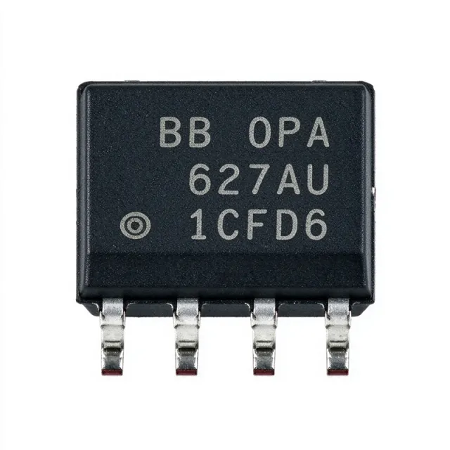
OPA627AU/2K5 - 16MHz Precision JFET Op Amp 55V/us | TI
部品番号: OPA627AU/2K5 ✓ 生産中| 数量 | 単価 | 小計 |
|---|---|---|
| 1 | $13.69 | $13.69 |
| 10 | $12.75 | $127.50 |
| 100 | $11.5 | $1,150.00 |
| 500 | $10.9 | $5,450.00 |
| 1,000 | $10.5 | $10,500.00 |
OPA627AU/2K5 概要
A JFET-input operational amplifier is a voltage-feedback amplifier whose input stage uses junction field-effect transistors to achieve extremely low input bias current and high input impedance. Within the signal-chain hierarchy, it sits under the operational amplifier family, itself a core analog building block of amplifier ICs and precision analog front-end design.
Key features include a very low offset voltage of 100 uV max, maximum drift of 0.8 uV/C, and input bias current as low as 5 pA max thanks to the DiFet (dielectrically isolated FET) input stage. The part is unity-gain stable, settling fast to 0.01% accuracy, and provides very low voltage noise at 10 kHz. Supply operation spans +-4.5 V to +-18 V, supporting both +-15 V industrial analog rails and +-5 V precision systems.
Technically, the OPA6x7 family is fabricated on a high-speed dielectrically isolated (DiFet) process, which gives the OPA627 lower noise, lower offset, and higher speed than the earlier OPA111 while retaining picoampere input currents. The sibling OPA637 shares the die but is stable only at gains of 5 or greater, trading stability margins for wider bandwidth at high gain.
Typical applications include precision data-acquisition front ends, photodiode transimpedance amplifiers, professional and audiophile audio preamplifiers, and test-and-measurement instrumentation where low offset drift and low bias current are decisive.
A key design consideration: because the part is unity-gain stable at 16 MHz, layout with short feedback traces and solid ground planes is essential to avoid parasitic ringing; for gains of 5 or more, the faster OPA637 is often the better choice.
This page synthesizes distributor pricing, drop-in alternatives, and practical design notes not found in the manufacturer datasheet.
ドロップイン代替品: OPA627AU/2K5 — 同一パッケージでピン互換。PCBの作り直しが必要な異なるパッケージの部品は除外されています。
このシリーズのバリエーション
同一シリーズでドロップイン互換のモデル: OPA627AU/2K5 (同一形状・フットプリント) — 相違点: Amplifier Type, Package.
クイック比較ツール — 並列比較する代替部品を選択:
OPA627AU
✓ 在庫あり
$12.1 / 個
データシートを見る →OPA637AU
✓ 在庫あり
$35.86 / 個
データシートを見る →OPA637AU/2K5
✓ 在庫あり
$17.6 / 個
データシートを見る →OPA627BP
✓ 在庫あり
$21.3 / 個
データシートを見る →OPA827AID
📋 参考代替品(カタログ未掲載)
OPA627AU/2K5 最大定格&電気的特性
| Amplifier Type | Precision high-speed JFET (DiFet) operational amplifier |
| Number of Channels | 1 |
| Unity-Gain Bandwidth | 16 MHz |
| Slew Rate | 55 V/us |
| Supply Voltage Range | +-4.5 V to +-18 V |
| Offset Voltage (max) | 100 uV |
| Offset Voltage Drift (max) | 0.8 uV/C |
| Input Bias Current (max) | 5 pA |
| Stability | Unity-gain stable |
| 動作温度範囲 | -25C to +85C |
| パッケージ | SOIC (D), 8 pins |
| 実装タイプ | Surface Mount |
| Packaging Suffix | /2K5 (Tape and Reel, 2500 units) |
| RoHS ステータス | Compliant (standard AU suffix non-E4); E4 variants explicitly RoHS per distributor data |
OPA627AU/2K5 ピン構成
| ピン 1 | TRIM (Offset Trim N) — Offset null trim terminal - connect to trim network or leave open |
| ピン 2 | -IN — Inverting input |
| ピン 3 | +IN — Non-inverting input |
| ピン 4 | V- — Negative supply |
| ピン 5 | TRIM (Offset Trim P) — Offset null trim terminal - connect to trim network or leave open |
| ピン 6 | OUT — Amplifier output |
| ピン 7 | V+ — Positive supply |
| ピン 8 | NC — Not connected (per datasheet) |
主な用途
OPA627AU/2K5 の用途: 6 件s: Precision Data Acquisition Front End, Photodiode Transimpedance Amplifier, High-End Audio Preamplifier and DAC Output Stage, Test and Measurement Instrumentation, Active Filter and Signal Conditioning, Medical and Biomedical Sensor Front Ends.
Precision Data Acquisition Front End
In precision data acquisition systems, the OPA627AU/2K5 buffers sensor and ADC inputs where DC accuracy directly defines system resolution. Its 100 uV max offset voltage and 0.8 uV/C max drift mean that over a 0-70C span the offset contributes under 100 uV of total error, negligible next to a 16-bit ADC LSB of 76 uV on a 5 V reference. The 5 pA max input bias current avoids loading high-impedance sources such as bridge transducers and pH probes with even megaohm source impedance. Placed as a unity-gain buffer directly ahead of successive-approximation ADCs, its 16 MHz bandwidth and 55 V/us slew rate allow it to settle driving dynamic input sampling without adding settling error; a small series resistor at the ADC pin isolates capacitive load transients.
おすすめ
Photodiode Transimpedance Amplifier
Photodiode current-to-voltage conversion demands an amplifier whose input bias current is far below the smallest photocurrent of interest. The OPA627AU/2K5's 5 pA max JFET bias current allows measuring currents down to hundreds of picoamperes with less than a few percent error, and its low input voltage noise limits output noise multiplied by the total input capacitance. With a 1 megaohm feedback resistor, each picoampere yields 1 uV of output, so bias-current-induced offset stays near 5 uV. The 16 MHz gain-bandwidth permits megahertz-range transimpedance bandwidths when feedback capacitance is chosen correctly; designers should add a feedback capacitor calculated from the photodiode junction capacitance to guarantee phase margin, using the OPA627's unity-gain stability as a safety margin.
おすすめ
High-End Audio Preamplifier and DAC Output Stage
The OPA627 family is a reference-grade choice in professional and audiophile audio: its JFET input presents high impedance to volume potentiometers and phono cartridges, while 55 V/us slew rate and 16 MHz bandwidth guarantee that full-scale 20 kHz signals are reproduced with negligible slewing-induced distortion. Very low voltage noise at 10 kHz keeps the noise floor below -110 dBu in typical preamp gains. In DAC output I/V conversion and active low-pass filtering, the unity-gain stability of the OPA627 makes it safe in Sallen-Key and multiple-feedback filter topologies where the OPA637 (stable only at gain >= 5) cannot be used. Community designs often pair one OPA627 per channel with a BUF634 inside the feedback loop to drive headphones or long cables.
おすすめ
Test and Measurement Instrumentation
Bench multimeters, oscilloscope front ends, and automated test equipment require amplifiers combining DC precision with fast settling. The OPA627AU/2K5 settles to 0.01% rapidly (fast settling listed among its core features) while contributing only 100 uV max offset and 0.8 uV/C drift, enabling ranges down to millivolts without auto-zero calibration. Its +-18 V supply rating allows signals riding on high common-mode voltages in legacy +-15 V systems. In programmable-gain front ends operating at gains of 5 or more, the pin-compatible OPA637 can be substituted on the same SOIC-8 footprint for extra high-gain bandwidth, letting one PCB layout serve both slow-precision and fast-acquisition product variants with a single bill-of-materials change.
おすすめ
Active Filter and Signal Conditioning
Active low-pass, band-pass, and anti-aliasing filters benefit from the OPA627AU/2K5's combination of 16 MHz bandwidth and unity-gain stability. In multiple-feedback topologies that present low, frequency-dependent noise gains, amplifiers that are only conditionally stable can oscillate; the OPA627's guaranteed unity-gain stability removes this risk. Its low bias current permits large resistor values (megaohm range) needed for audio and biomedical filter time constants without bias-current-induced offset errors, and the JFET input's low current noise keeps resistor-noise-dominated designs unaffected. Designers should verify that closed-loop noise gain stays above the unity-gain crossover's phase-margin requirements and keep feedback capacitor values small to preserve the intended pole frequencies.
おすすめ
Medical and Biomedical Sensor Front Ends
Biopotential and physiological sensor interfaces - ECG, EEG, photoplethysmography, and lab-scale photometry - require amplifiers that neither load fragile electrodes nor inject offset drift into sub-millivolt signals. The OPA627AU/2K5's 5 pA max bias current and megaohm-level input impedance preserve electrode polarization conditions, while 0.8 uV/C drift keeps baseline wander negligible relative to typical 1 mV ECG amplitudes even across body-temperature swings. Its wide +-4.5 V to +-18 V supply range supports medically conventional +-5 V and +-12 V rails. Used as the first gain block ahead of an instrumentation amplifier or an ADC such as the CS5534, it provides high input headroom and slew capability for transient artifacts; patient-isolation requirements are handled by upstream isolation barriers, not the amplifier itself.
おすすめ
おすすめ製品の概要
エンジニアリング参考データ: OPA627AU/2K5 — 比較、設計ガイダンス、コンプライアンス情報。
選定ガイド
代替品との比較
| パラメータ | この製品 | OPA627AU | OPA637AU | OPA637AU/2K5 | OPA627BP | OPA827AID |
|---|---|---|---|---|---|---|
| Package | SOIC-8 (D) | SOIC-8 (D) - same | SOIC-8 (D) - same | SOIC-8 (D) - same | SOIC-8 (D) - same | SOIC-8 (D) - same |
| Brand | Texas Instruments | Texas Instruments | Texas Instruments | Texas Instruments | Texas Instruments | Texas Instruments |
| Stability | Unity-gain stable | Unity-gain stable | Stable at gain >= 5 only | Stable at gain >= 5 only | Unity-gain stable | Unity-gain stable |
主な差別化要因
- Unity-gain stability at 16 MHz (vs OPA637AU)
- Ultra-low drift for uncalibrated precision (vs OPA827AID)
- 5 pA max input bias current (vs OPA627AU (equivalent) and bipolar-input precision amps)
設計ノート
Decouple V+ (pin 7) and V- (pin 4) with 0.1 uF ceramic capacitors placed within 2-3 mm of the pins, plus 4.7-10 uF bulk capacitance per rail. The OPA627 operates from +-4.5 V to +-18 V; exceeding +-18 V damages the JFET input stage. Reverse-supply protection with series resistors or Schottky clamps is recommended in systems with uncertain power-up sequencing. Quiescent current is modest but the SOIC-8 thermal path limits sustained output drive into heavy loads - Estimated: at 36 V total span with 20 mA load, package dissipation is roughly 0.72 W, so verify junction temperature against the SOIC-8 theta_JA.
With 16 MHz of bandwidth, keep the feedback loop as short as possible and avoid routing the summing junction under high-slew digital traces. Place the feedback resistor directly across pins 2 and 6 with minimal pad area at the inverting input to reduce stray capacitance, which causes gain peaking in transimpedance circuits. Use a solid ground plane and return load currents away from the input ground reference. The offset trim pins (1 and 5) should be left unconnected if trimming is not used - never float trim networks mid-circuit during operation.
The most frequent substitution error is using the OPA637 where an OPA627 is required: the OPA637 is stable only at closed-loop gains of 5 or greater and will oscillate in unity-gain buffers, followers, and MFB filters. Conversely, designers needing maximum high-gain bandwidth should choose the OPA637 on the same footprint. Also note the /2K5 suffix is a packaging code (2500-unit tape and reel), not a different grade - ordering OPA627AU in tube yields the identical die. Finally, this grade is rated -25C to +85C; full industrial -40C designs need grade verification.
コンプライアンス情報
Abacus Technologies lists OPA627AU family as EU RoHS compliant, REACH compliant, PFAS: NO, DRC conflict free; explicit status for the exact /2K5 suffix should be confirmed on the TI product page.





