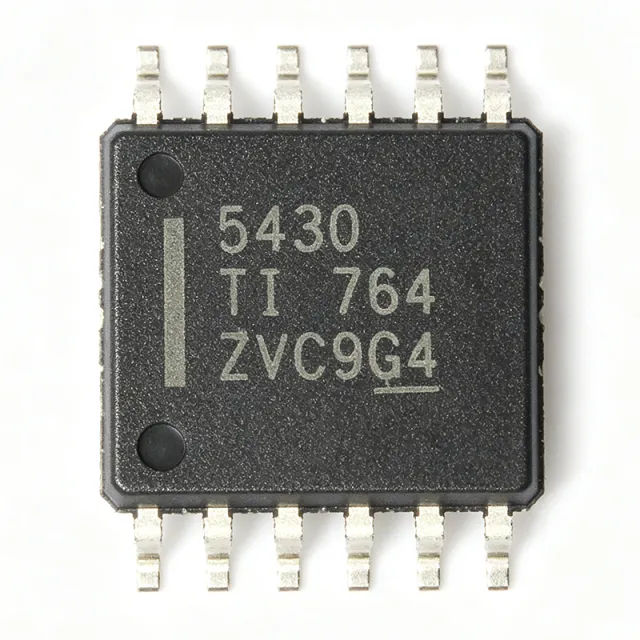
TPS5430DDAR - 3A、36V降圧コンバータ | Texas Instruments
部品番号: TPS5430DDAR ✓ 生産中| 数量 | 単価 | 小計 |
|---|---|---|
| 1 | $2.15 | $2.15 |
| 10 | $1.93 | $19.30 |
| 100 | $1.62 | $162.00 |
| 500 | $1.38 | $690.00 |
| 1,000 | $1.19 | $1,190.00 |
TPS5430DDAR 概要
バックコンバータは、スイッチングMOSFET、インダクタ、出力コンデンサを使用して、より高いDC電圧をより低い電圧に効率的に降圧するスイッチング電圧レギュレータの一種です。リニアレギュレータとは異なり、スイッチングコンバータは通常90%を超える効率を達成し、現代の電源管理IC階層(DC-DCコンバータ -> スイッチングレギュレータ -> ポイント・オブ・ロードコンバータ)の基盤となっています。TPS5430は、TIのSWIFTファミリのDC-DCコンバータに属します。
主な特長は、12Vおよび24Vの産業用・車載バスを直接受け付ける5.5V~36Vの入力範囲、3Aの連続出力電流、小型インダクタを可能にする固定500kHz動作、統合ハイサイドNチャネルMOSFET、内部ループ補償、ソフトスタート、サイクル・バイ・サイクル電流制限、熱シャットダウンです。熱強化SO-8 PowerPADパッケージは、外部ヒートシンクなしで全負荷動作を可能にする低熱抵抗を提供します。
このデバイスは、内部1.221Vバンドギャップリファレンスを備えたPWM電圧モード制御を使用します。出力電圧はVSENSEピンの外部分圧抵抗によって設定されます。BOOTとPH間のブートストラップコンデンサが、ハイサイドMOSFETゲートをVIN以上に駆動します。固定周波数動作は、可変周波数コンバータと比較してEMIフィルタ設計を簡素化します。
一般的なアプリケーションには、FPGA、DSP、マイクロコントローラ用のポイント・オブ・ロード電源、24V産業用バス電源、通信中間レール、12V車載アクセサリ電源、5V/3.3V分散電源システムが含まれます。
設計のヒント:入力/出力コンデンサとブートストラップコンデンサをICの近くに配置し、PowerPADをサーマルビア付きの銅箔に半田付けし、PHスイッチングノードと電力ループを短く保ってリンギングとEMIを最小限に抑えます。
ドロップイン代替品: TPS5430DDAR — 同一パッケージでピン互換。PCBの作り直しが必要な異なるパッケージの部品は除外されています。
このシリーズのバリエーション
同一シリーズでドロップイン互換のモデル: TPS5430DDAR (同一形状・フットプリント) — 相違点: Topology, Output Voltage Range, Package, Input Voltage Range, Control Method.
クイック比較ツール — 並列比較する代替部品を選択:
TPS5430DDA
✅ ドロップイン📋 参考代替品(カタログ未掲載)
TPS5430DDAG4
✅ ドロップイン📋 参考代替品(カタログ未掲載)
TPS5430QDDARQ1
✅ ドロップイン✓ 在庫あり
$1.95 / 個
データシートを見る →TPS5450DDAR
✅ ドロップイン✓ 在庫あり
$2.55 / 個
データシートを見る →TPS54331DR
⚡ 同一パッケージ✓ 在庫あり
$0.85 / 個
データシートを見る →MP1584EN
⚡ 同一パッケージ📋 参考代替品(カタログ未掲載)
RT8279GSP
⚡ 同一パッケージ📋 参考代替品(カタログ未掲載)
TPS5430DDAR 最大定格&電気的特性
| トポロジー | Step-Down (Buck) |
| 入力電圧範囲 | 5.5 V to 36 V |
| 出力電圧 | Adjustable, 1.221 V to near VIN |
| 最大出力電流 | 3 A |
| スイッチング周波数 | 500 kHz (fixed) |
| 基準電圧 | 1.221 V |
| Control Topology | Voltage-mode PWM |
| MOSFET | Integrated high-side N-channel |
| Protection Features | Cycle-by-cycle current limit, thermal shutdown, soft-start |
| 出力数 | 1 |
| パッケージ | 8-PowerSOIC (DDA), PowerPAD, 0.154 in / 3.90 mm width |
| 実装タイプ | Surface Mount |
| Packaging | Tape & Reel (R suffix) |
| RoHS ステータス | Compliant |
| Family | TI SWIFT DC-DC converters |
TPS5430DDAR ピン構成
| ピン 1 | BOOT — Bootstrap capacitor connection to PH for high-side gate drive |
| ピン 2 | NC/GND — No connect / ground per datasheet layout |
| ピン 3 | VSENSE — Feedback input from output voltage divider (1.221V reference) |
| ピン 4 | ENA — Enable input, active high |
| ピン 5 | SS/TR — Soft-start / tracking programming pin |
| ピン 6 | GND — Ground reference (PowerPAD also ground) |
| ピン 7 | VIN — Input supply, 5.5V to 36V |
| ピン 8 | PH — Phase / switch node to inductor |
主な用途
TPS5430DDAR の用途: 6 件s: 24V Industrial Bus Point-of-Load, 12V Automotive Accessory Power, FPGA/DSP Point-of-Load Supply, Telecom Intermediate Rail Conversion, Distributed 5V/3.3V Power Systems, Battery-Powered and Portable Instrumentation.
24V Industrial Bus Point-of-Load
The TPS5430DDAR's 5.5V to 36V input range directly accepts 24V industrial control buses with transient headroom, eliminating a pre-regulator stage. Delivering 3A at a fixed 500kHz, it powers PLC I/O modules, sensors, and motor-drive logic rails. Internal compensation and fixed-frequency PWM simplify EMI filter design, while cycle-by-cycle current limit protects against shorted loads on long factory wiring. Its 1.221V reference allows any intermediate rail from 1.22V upward.
おすすめ
12V Automotive Accessory Power
For 12V automotive accessory rails, the 36V maximum input covers load-dump-adjacent conditions in protected front ends, and the automotive-qualified TPS5430QDDARQ1 variant (same footprint) supports AEC-Q100 programs. The 3A output supplies infotainment sub-rails, telematics, and body-electronics processors at 5V or 3.3V with efficiency above 90%, reducing thermal load in sealed enclosures. Fixed 500kHz switching keeps inductors small for space-constrained modules.
おすすめ
FPGA/DSP Point-of-Load Supply
The TPS5430DDAR provides 3A core and I/O rails for FPGAs, DSPs, and microcontrollers from 5V or 12V intermediates. Its soft-start pin enables controlled inrush for high ceramic capacitance, and the 500kHz fixed frequency allows inductors in the 10-15uH class with fast transient response for logic load steps. The 1.221V reference supports modern low-voltage cores, and the PowerPAD package dissipates conversion losses without a heatsink at typical 2-3A loads.
おすすめ
Telecom Intermediate Rail Conversion
In telecom and networking equipment, the TPS5430DDAR converts intermediate distribution voltages down to point-of-load rails with 90%+ efficiency. The 36V input tolerates -48V-derived rails after a step-down front end, and the wide input range allows one BOM across 12V, 15V, and 24V shelves. The thermal shutdown and hiccup-style current limit protect against fan-failure thermal events common in telecom cabinets, while the SO-8 PowerPAD suits high-density line-card layouts.
おすすめ
Distributed 5V/3.3V Power Systems
For distributed power architectures, the TPS5430DDAR generates 5V or 3.3V logic rails from upstream intermediates at a fixed 500kHz, so ripple falls in a predictable band that standard LC filters attenuate easily. Voltage-mode PWM with internal compensation reduces external component count to an inductor, two divider resistors, and input/output capacitors, cutting BOM cost. The adjustable output and 3A capacity cover backplane-fed subsystems, industrial gateways, and test-instrument auxiliaries.
おすすめ
Battery-Powered and Portable Instrumentation
Portable instruments powered by 12V lead-acid or multi-cell Li-ion packs benefit from the TPS5430DDAR's wide 5.5V-36V input that spans battery discharge curves. Fixed-frequency 500kHz operation keeps the converter out of audible bands and enables magnetics small enough for handheld enclosures, while better than 90% efficiency extends runtime. Thermal shutdown protects against blocked ventilation, and the SS pin can sequence the analog front end after the digital core.
おすすめ
おすすめ製品の概要
エンジニアリング参考データ: TPS5430DDAR — 比較、設計ガイダンス、コンプライアンス情報。
選定ガイド
代替品との比較
| パラメータ | この製品 | TPS5430DDA | TPS5430QDDARQ1 | TPS5450DDAR | TPS54331DR |
|---|---|---|---|---|---|
| Package | 8-PowerSOIC (DDA) | 8-PowerSOIC (DDA) - same | 8-PowerSOIC (DDA) - same | 8-PowerSOIC (DDA) - same | SOIC-8 - different pinout |
| Brand | Texas Instruments | Texas Instruments | Texas Instruments | Texas Instruments | MPS |
| Input Voltage Range | 5.5V to 36V | 5.5V to 36V | 5.5V to 36V | 5.5V to 36V | 4.5V to 28V |
| Output Current | 3 A | 3 A | 3 A | 5 A | 1.5 A |
| Switching Frequency | 500 kHz | 500 kHz | 500 kHz | 500 kHz | 1.5 MHz (adjustable) |
| Automotive Grade | No | No | Yes (AEC-Q100) | No (Q1 version available) | No |
| Reference Voltage | 1.221 V | 1.221 V | 1.221 V | 1.221 V | 0.8 V |
| Approx. Price (1 pc, as of 2026-08-29) | $2.15 | $2.15 | $2.50 | $3.10 | $0.60 |
主な差別化要因
- クラシックSWIFT SO-8ファミリで最も広い入力範囲 (vs TPS54331DR)
- ピン互換5Aアップグレードパス (vs TPS5450DDAR)
- クロスブランド同等品より高い出力電流 (vs MP1584EN)
- 車載認定バリアントが利用可能 (vs TPS5430DDA)
設計ノート
SO-8 PowerPADは熱性能に不可欠です:パッドを内部プレーンへのサーマルビアアレイ(通常1.0mmピッチで3x3)を備えたグランドプレーンに半田付けします。12Vinから3.3V/3A出力時、消費電力は約2Wです。堅牢なPowerPAD接続がないと、ジャンクション温度が制限を超える可能性があります。TIデータシートのEVM熱レイアウトに従ってください。
入力コンデンサ、PHピン、フリーホイーリングダイオードのグランドループをできるだけ短く広く保ちます - これが高di/dtホットループです。BOOTコンデンサ(0.01uF)をBOOTピンとPHピンの間に直接配置します。VSENSEフィードバックトレースをPHとインダクタから遠ざけて配線し、スイッチングノイズがレギュレーションを損なわないようにします。
PHピンはデッドタイム中にVINとグランド未満の間でスイッチングします - 適切な外部ショットキーダイオードを使用し、VINの36V絶対最大定格を超えないようにしてください。大きなセラミック出力バンクでの起動時に電流制限フォールドバックを防ぐため、負荷容量に応じてソフトスタート容量を設定します。抵抗分圧器の公差(1%)を確認して出力を仕様内に保ちます。
固定500kHz動作は予測可能な高調波を生成します - リンギングが部品定格を超える場合はPHからグランドへ小さなRCスナバを追加します。24V産業用バスでの伝導エミッションを満たすためにパイ入力フィルタが必要になる場合があります。固定周波数(MP1584ENのような可変周波数部品と比較して)はフィルタ設計を簡単にします。
コンプライアンス情報
RoHS compliant per DigiKey product listing (non-G4 suffix indicates standard RoHS-compliant TI ordering). AEC-Q100 not applicable to standard part - use TPS5430QDDARQ1 for automotive qualification.







