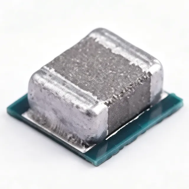
TPS82130SILR - 17V 3A 降圧MicroSiPモジュール | Texas Instruments
部品番号: TPS82130SILR ✓ 生産中| 数量 | 単価 | 小計 |
|---|---|---|
| 1 | $3.44 | $3.44 |
| 10 | $3.1 | $31.00 |
| 100 | $2.75 | $275.00 |
| 500 | $2.45 | $1,225.00 |
| 1,000 | $2.18 | $2,180.00 |
TPS82130SILR 概要
降圧コンバータはバックコンバータとも呼ばれ、高い入力電圧を高効率で低い出力電圧に変換するスイッチングDC-DC電圧レギュレータです。バックコンバータは電源管理IC階層の核となる構成要素であり、LDO、チャージポンプ、電源モジュールと並んで位置づけられます。TPS82130はさらに、ディスクリートのスイッチングFET、インダクタ、ループ補償を単一のマイクロモジュールに集約し、外部FET、パワーインダクタ、補償部品を必要とするディスクリートレギュレータ設計と比較して、外付け部品点数とPCB面積を大幅に削減します。
主な特長は、12Vおよび5Vバスシステムをサポートする広い3V~17V入力範囲、3A連続出力、外付け抵抗分圧による0.9V~5Vの調整可能出力、小さな外付けコンデンサを可能にする2.2MHz固定スイッチング周波数、突入電流制限のための内部ソフトスタート、シーケンス用のパワーグッド出力フラグ、シャットダウン制御用のイネーブルピン、熱シャットダウン保護です。MicroSiPパッケージは底面サーマルパッドを露出し、熱を直接PCBの銅箔に逃がします。
技術的には、TPS82130は固定周波数ピーク電流モード制御を採用し、最小限の出力容量(通常22uFセラミック)で高速過渡応答と安定性を提供します。高いVIN対VOUT比での低ドロップアウトのために100%デューティサイクル動作をサポートします。統合シールドインダクタは放射EMIを低減しながらPCBレイアウトを簡素化し、低い1.5mmプロファイルは標準的な表面実装装置による自動組立に適しています。
一般的なアプリケーションには、産業システムにおけるFPGA、DSP、ASIC向けのポイントオブロード(POL)電源、ファクトリオートメーションのセンサー電源、IoTエッジノードにおける12Vレール分散電源、小型ソリューションサイズが重要なポータブル試験装置などがあります。
設計時は、入出力セラミック容量に関するデータシートの推奨事項に従い、モジュールを負荷の近くに配置し、特に高出力電流時にはサーマルパッド下に十分な銅面積を確保してください。価格の参考値は2026-08-28時点で適用されます。
このページは、ディストリビュータの価格、ドロップイン代替品、およびメーカーのデータシートには記載されていない実用的な設計ノートをまとめたものです。
ドロップイン代替品: TPS82130SILR — 同一パッケージでピン互換。PCBの作り直しが必要な異なるパッケージの部品は除外されています。
このシリーズのバリエーション
同一シリーズでドロップイン互換のモデル: TPS82130SILR (同一形状・フットプリント) — 相違点: Continuous Output Current, MSL Level, Output Voltage Range, Package, Switching Frequency.
クイック比較ツール — 並列比較する代替部品を選択:
TPS82140SILR
✅ ドロップイン✓ 在庫あり
$2.45 / 個
データシートを見る →TPS82150SILR
✅ ドロップイン📋 参考代替品(カタログ未掲載)
TPS82130SILT
✅ ドロップイン📋 参考代替品(カタログ未掲載)
TPS82130SILR 最大定格&電気的特性
| トポロジー | Synchronous Buck (Step-Down) |
| Module Type | MicroSiP Power Module (integrated inductor and FETs) |
| 入力電圧範囲 | 3 V to 17 V |
| 出力電圧範囲 | 0.9 V to 5 V (adjustable) |
| Continuous Output Current | 3 A |
| スイッチング周波数 | 2.2 MHz (typical, fixed) |
| Control Mode | Peak Current Mode |
| Efficiency (typical) | >90% at moderate load |
| ソフトスタート | Internal |
| パワーグッド出力 | Yes |
| イネーブルピン | Yes (active-high) |
| 熱シャットダウン | Yes |
| 動作温度範囲 | -40C to +125C |
| パッケージ | 8-pin uSIP (SIL) 3.0mm x 2.8mm x 1.5mm |
| 実装タイプ | Surface Mount |
| MSLレベル | 2 (1 year floor life) |
| RoHS ステータス | Compliant |
TPS82130SILR ピン構成
| ピン 1 | VIN — Input supply voltage |
| ピン 2 | GND — Signal ground |
| ピン 3 | EN — Enable input (active high) |
| ピン 4 | PGND — Power ground |
| ピン 5 | FB — Feedback voltage input |
| ピン 6 | VOUT — Regulated output voltage |
| ピン 7 | PG — Power good output flag |
| ピン 8 | AGND — Analog ground |
主な用途
TPS82130SILR の用途: 6 件s: FPGA Point-of-Load Power, Industrial Sensor and PLC Supplies, IoT Edge Devices and Gateway Nodes, Portable Test and Measurement Equipment, DSP and ASIC Core Power, Communication Equipment Power.
FPGA Point-of-Load Power
The TPS82130SILR is an ideal point-of-load supply for FPGA core and auxiliary rails in industrial embedded systems. With 3A continuous output, 0.9V to 5V adjustable output range, and a 3.0mm x 2.8mm uSIP footprint, it can power the FPGA core (typically 1.0V-1.2V), auxiliary (1.8V), and I/O (2.5V or 3.3V) rails from a single 12V bus. The 2.2MHz switching frequency avoids interfering with common FPGA clock harmonics around 100-500MHz, eliminating beat-frequency noise issues that plague lower-frequency regulators. Integrated synchronous FETs and shielded inductor eliminate 6-8 discrete components, dramatically reducing PCB area versus discrete buck designs.
おすすめ
Industrial Sensor and PLC Supplies
The TPS82130SILR powers industrial 4-20mA loop transmitters, PLC analog input modules, and 24V-bus sensor conditioning circuits. Its 3V-17V input range directly accepts the 24V industrial bus (after protection/regulation) and 12V backplane rails commonly used in factory automation. The wide operating temperature range of -40C to +125C supports deployment in unconditioned factory environments. With internal thermal shutdown, power-good output, and enable pin for power sequencing, the TPS82130 provides the robustness required for industrial IEC 61010 environments. Typical efficiency above 90% minimizes thermal dissipation in sealed enclosures.
おすすめ
IoT Edge Devices and Gateway Nodes
The TPS82130SILR fits compact IoT edge nodes and gateway designs that require multiple voltage rails in a small footprint. The integrated MicroSiP package occupies 75% less PCB area than equivalent discrete buck designs, freeing space for wireless modules, sensors, and battery management. With 3A peak capability, the TPS82130 can power a small SoC plus Wi-Fi/BLE radio module directly from a 12V or USB-C input. The 2.2MHz switching frequency enables small ceramic output capacitors (typically 22uF), and the internal soft-start limits inrush current that could trip upstream USB current-limit switches.
おすすめ
Portable Test and Measurement Equipment
Handheld oscilloscopes, data loggers, and field test equipment benefit from the TPS82130SILR's compact size, high efficiency, and wide input range. Battery-powered instruments often use a 2-cell or 3-cell Li-ion pack (6V-12.6V) that maps directly to the TPS82130 input range. The 3A continuous capability powers analog front-end ADCs, FPGAs, and display backlight drivers simultaneously. The 1.5mm low-profile uSIP package allows the entire power tree to fit on the back side of small PCBs, leaving the top side for analog signal paths and user interface components. High efficiency above 90% extends battery runtime.
おすすめ
DSP and ASIC Core Power
The TPS82130SILR is well-suited as a POL supply for DSP, ASIC, and high-performance microcontroller core rails. Modern DSPs often require 1.0V to 1.2V at 2-3A peak current with tight transient response - the TPS82130's peak-current-mode control delivers fast transient response with minimal output capacitance. The adjustable output from 0.9V to 5V covers virtually all DSP/ASIC core voltage requirements. The integrated power-good output enables sequencing with other system rails, and the enable pin allows shutdown to microampere-level quiescent current for sleep-mode applications. According to TI datasheet, the device supports 100% duty cycle for low-dropout operation at high VIN-VOUT deltas.
おすすめ
Communication Equipment Power
Networking switches, wireless base stations, and small cell radio units can use the TPS82130SILR to power digital signal processors and baseband chips from 12V backplane rails. The 2.2MHz switching frequency and integrated shielded inductor minimize radiated EMI - critical for communication equipment that must meet FCC and CE conducted/radiated emissions limits. With 3A output capability, the TPS82130 powers baseband SoCs and DDR memory termination rails simultaneously. The small MicroSiP footprint allows power circuits to be placed directly beneath or adjacent to the load IC, minimizing parasitic inductance and improving transient response.
おすすめ
おすすめ製品の概要
エンジニアリング参考データ: TPS82130SILR — 比較、設計ガイダンス、コンプライアンス情報。
選定ガイド
代替品との比較
| パラメータ | この製品 | TPS82140SILR | TPS82150SILR | TPS82130SILT |
|---|---|---|---|---|
| Package | 8-pin uSIP (SIL) 3.0x2.8mm | 8-pin uSIP (SIL) 3.0x2.8mm - same | 8-pin uSIP (SIL) 3.0x2.8mm - same | 8-pin uSIP (SIL) 3.0x2.8mm - same |
| Brand | Texas Instruments | Texas Instruments | Texas Instruments | Texas Instruments |
| Output Current | 3 A | 2 A | 1 A | 3 A |
| Input Voltage Range | 3 V to 17 V | 3 V to 17 V | 3 V to 17 V | 3 V to 17 V |
| Output Voltage Range | 0.9 V to 5 V | 0.9 V to 5 V | 0.9 V to 5 V | 0.9 V to 5 V |
| Switching Frequency | 2.2 MHz | 2.2 MHz | 2.2 MHz | 2.2 MHz |
| Module Type | MicroSiP (integrated inductor) | MicroSiP (integrated inductor) | MicroSiP (integrated inductor) | MicroSiP (integrated inductor) |
主な差別化要因
- TPS821xx uSIPファミリで最高の出力電流 (vs TPS82140SILR)
- 同一フットプリントでコストダウン設計向けの低電流 (vs TPS82150SILR)
- 統合MicroSiPパッケージが6-8個のディスクリート部品を排除 (vs ディスクリートTPS54360バック設計)
設計ノート
推定:VIN=12V、VOUT=3.3V、3A負荷時、TPS82130SILRは約(12-3.3) x 3 = 26.1 Wの電力を消費します。底面サーマルパッドに十分な銅箔(データシートは最小フットプリントパターンを推奨)があれば、ジャンクション-アンビエント間熱抵抗は通常約30-40 C/Wとなり、周囲温度より50-80 C上昇します。連続3A動作では、データシートのリファレンスレイアウトパターンに正確に従い、パッケージの露出パッド下に複数のサーマルビアを使用して熱をPCB内層に移動させてください。
TPS82130SILRモジュールは負荷ICの近く、理想的には5-10mm以内に配置し、出力ループの寄生インダクタンスを最小化してください。VIN、VOUT、PGND、および露出サーマルパッドには広い銅箔(少なくとも50mil)を使用してください。TIデータシートのレイアウトガイドラインに従い、入力セラミックコンデンサ(通常22uF X7R)をVINピンにできるだけ近づけ、出力セラミックコンデンサ(通常22uF X7R)をVOUTピンに直接配置してください。AGNDピンは、出力コンデンサのグランドリターン付近の1点でPGND銅箔に接続する必要があります。
TPS82130SILRを絶対最大VINの17V以上で動作させないでください。12V産業バスの過渡電圧はホットプラグ時にこれを超える可能性があります。設計が長い外部ケーブルに接続される場合は、TVSダイオードまたは入力電圧クランプを追加してください。入力コンデンサを省略しないでください。TPS82130の高いdi/dtスイッチングには、VINリンギングを防ぐために低ESRセラミック入力キャップが必要です。データシートに従い、X7R/X5Rセラミックコンデンサを使用してください。DCバイアスと温度で公称容量の60-80%を失うY5Vに置き換えないでください。
FB(フィードバック)トレースをノイズの多いスイッチングノード(VIN、PGND、VOUT)から遠ざけ、出力コンデンサの上部からFBピンへ直接、グランド銅箔に囲まれた短く細いトレースで配線してください。フィードバック分圧抵抗をインダクタの近くに配置しないでください。磁気結合がフィードバック経路にノイズを注入し、出力リップルや不安定性を引き起こす可能性があります。PG(パワーグッド)出力はオープンドレイン信号であり、VOUTまたはロジックレールへの外付けプルアップ抵抗(通常10k-100k)が必要です。
コンプライアンス情報
RoHS and REACH compliant per TI product page. Not AEC-Q100 qualified; choose TPS62150A-Q1 or similar -Q1 part for automotive applications.







