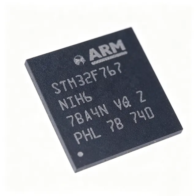
STM32F767NIH6 - 32-bit ARM Cortex-M7 MCU, 2MB Flash, 216MHz | STMicroelectronics
部品番号: STM32F767NIH6 ✓ 生産中| 数量 | 単価 | 小計 |
|---|---|---|
| 1 | $16.8 | $16.80 |
| 10 | $15.2 | $152.00 |
| 100 | $13.55 | $1,355.00 |
| 500 | $12.1 | $6,050.00 |
| 1,000 | $10.85 | $10,850.00 |
STM32F767NIH6 概要
What is a microcontroller? A microcontroller (MCU) is a compact integrated circuit that combines a processor core, on-chip memory (Flash and SRAM), and programmable I/O peripherals on a single die, intended to govern a specific operation in an embedded system. Microcontrollers are the backbone of embedded designs ranging from simple motor controllers to complex IoT gateways. The STM32F767NIH6 belongs to the STM32F7 series, a high-performance family within the broader STM32 ecosystem positioned for graphics-rich HMI, motor control, and audio processing where Cortex-M4 class performance is insufficient.
Key features of the STM32F767NIH6 include 4x I2C, 4x USART, 4x UART, 6x SPI, 3x CAN, 2x USB OTG, 1x Ethernet MAC, 1x SDMMC, a 16-bit ADC at 3.6 MSPS, a 12-bit DAC, hardware AES/3DES/DES cryptographic engines, a true random number generator (TRNG), 159 I/O lines, a 32-bit external data bus, and a 26-bit address bus. The device also integrates a JPEG codec, DFSDM (digital filter for sigma-delta modulators), and a TFT LCD controller for direct display driving without external graphics RAM.
Technically, the STM32F767NIH6 uses an ART Accelerator with branch prediction and a 6-stage pipeline to maintain 0-wait-state Flash access at full 216 MHz, while dual-bank Flash supports read-while-write firmware updates. The MPU, separate instruction and data caches, and DSP extensions allow real-time DSP workloads alongside control tasks. The device operates from 1.7V to 3.6V across -40C to +85C (industrial grade) and offers multiple low-power modes.
Typical applications include industrial control systems, motor drives, IoT gateways, human-machine interfaces (HMIs) with TFT displays, audio processing, and high-end consumer electronics. The combination of 216 MHz performance, large memory, and rich peripherals makes it ideal for applications that demand real-time processing and connectivity.
When designing with this MCU, ensure proper decoupling of the power supply pins and a stable clock source. The device supports multiple boot modes and has a flexible power management scheme with multiple low-power modes. For high-speed interfaces like Ethernet and USB, careful PCB layout is essential to maintain signal integrity.
This page synthesizes distributor pricing, drop-in alternatives, and practical design notes not found in the manufacturer datasheet, plus comparison tables and AEO-optimized application guidance.
ドロップイン代替品: STM32F767NIH6 — 同一パッケージでピン互換。PCBの作り直しが必要な異なるパッケージの部品は除外されています。
このシリーズのバリエーション
同一シリーズでドロップイン互換のモデル: STM32F767NIH6 (同一形状・フットプリント) — 相違点: Package, Operating Temperature, Core, SRAM, Timers.
クイック比較ツール — 並列比較する代替部品を選択:
STM32F769NIH6
✅ ドロップイン✓ 在庫あり
$15.85 / 個
データシートを見る →STM32F767IIT6
✅ ドロップイン✓ 在庫あり
$11.95 / 個
データシートを見る →STM32F767BIT6
✅ ドロップイン✓ 在庫あり
$11.85 / 個
データシートを見る →STM32F765ZIT6
✅ ドロップイン✓ 在庫あり
$10.95 / 個
データシートを見る →STM32F779BIT6
✅ ドロップイン✓ 在庫あり
$11.75 / 個
データシートを見る →STM32F479NIH6
✅ ドロップイン✓ 在庫あり
$11.75 / 個
データシートを見る →STM32F767NIH6 最大定格&電気的特性
| Core | Arm 32-bit Cortex-M7 with double-precision FPU |
| 最大クロック周波数 | 216 MHz |
| CoreMark / DMIPS | 462 DMIPS / 2.14 DMIPS/MHz (Dhrystone 2.1) |
| Cache | 16 Kbytes I/D L1-cache |
| Program Memory Size | 2 MB Flash (dual-bank) |
| RAM Memory Size | 512 KB SRAM |
| Operating Voltage Range | 1.7 V to 3.6 V |
| 動作温度範囲 | -40 C to +85 C (industrial grade) |
| Number of I/O Lines | 159 |
| External Data Bus | 32-bit |
| External Address Bus | 26-bit |
| パッケージ | TFBGA-216 (13x13mm, 0.8mm pitch) |
| I2C Interfaces | 4 |
| UART / USART | 4 USART + 4 UART |
| SPI Interfaces | 6 |
| CAN Interfaces | 3 |
| USB Interfaces | 2x USB OTG |
| Ethernet | 1x 10/100 MAC |
| SDMMC | 1x |
| ADC | 16-bit, up to 3.6 MSPS |
| DAC | 12-bit |
| Cryptography | AES, DES, 3DES, TRNG |
| Graphics | Chrom-ART Accelerator, TFT LCD controller, JPEG codec |
| DSP | Yes (DSP instructions) |
| RoHS ステータス | Compliant |
STM32F767NIH6 ピン構成
| ピン A1 | VSS — Digital ground |
| ピン A2 | PE0 — GPIO PE0 / TIM4_ETR |
| ピン B1 | VDD — Digital power 1.7-3.6V |
| ピン F12 | BOOT0 — Boot mode select |
| ピン L1 | NRST — Reset (active low) |
| ピン N12 | VBAT — RTC backup supply |
| ピン D11 | OSC_IN — HSE oscillator input |
| ピン D12 | OSC_OUT — HSE oscillator output |
| ピン K12 | PA13 — SWDIO (debug data) |
| ピン L12 | PA14 — SWCLK (debug clock) |
| ピン G1 | PD0 — OSC_IN for 32 kHz |
| ピン G2 | PD1 — OSC_OUT for 32 kHz |
主な用途
STM32F767NIH6 の用途: 7 件s: Human-Machine Interface (HMI) with TFT Display, Industrial Motor Control and Drives, IoT Gateway and Edge Connectivity, Audio Processing and Codec Bridging, High-End Consumer Electronics, Test and Measurement Instrumentation, Medical Device User Interfaces.
Human-Machine Interface (HMI) with TFT Display
The STM32F767NIH6 is ideal for graphics-rich HMI panels thanks to its Cortex-M7 core at 216 MHz, integrated TFT LCD controller, and Chrom-ART Accelerator that offloads 2D graphics operations. With 2 MB of dual-bank Flash and 512 KB SRAM, the MCU can run LVGL or STemWin stacks while maintaining responsive touch input. Designers connect a TFT panel via the integrated RGB888 interface and route capacitive touch via I2C, with the JPEG codec accelerating image decoding for splash screens and icons. Compared to a discrete display controller + MCU solution, the F767NIH6 removes the external controller BOM and reduces PCB complexity in industrial control panels and home appliance UIs.
おすすめ
Industrial Motor Control and Drives
In field-oriented control (FOC) applications, the STM32F767NIH6 delivers deterministic DSP performance via Cortex-M7 at 216 MHz and DSP instructions, plus a 16-bit ADC sampling at 3.6 MSPS for current sensing. Three CAN interfaces support CANopen and CiA 402 drive profiles, while the advanced timers provide center-aligned PWM for three-phase bridges. ST's MC SDK and Motor Control Workbench tooling target this part directly, with reference firmware reaching 30 kHz FOC loops. The 512 KB SRAM and 2 MB Flash allow sensorless and encoder-based algorithms to coexist with safety logic, making the F767NIH6 a strong fit for servo drives, pumps, and industrial automation controllers.
おすすめ
IoT Gateway and Edge Connectivity
The STM32F767NIH6 suits industrial IoT gateways because it integrates a 10/100 Ethernet MAC, dual USB OTG (host/device), SDMMC for SD-card storage, and multiple SPI/I2C/UART channels for sensor and modem interfaces. The Cortex-M7 at 216 MHz with 2 MB Flash can host TLS, MQTT, OPC UA, or LwM2M stacks while still servicing local sensor polling. DFSDM channels support sigma-delta MEMS microphones or industrial sensors directly. Compared to MCU + external TCP/IP offload solutions, the F767NIH6 simplifies BOM and accelerates time-to-market for gateways aggregating Modbus, BACnet, and CAN fieldbus data on the factory floor.
おすすめ
Audio Processing and Codec Bridging
Audio applications benefit from the STM32F767NIH6's Cortex-M7 with DSP instructions at 216 MHz, hardware AES/3DES for DRM decryption, and DFSDM channels for digital microphone arrays. The integrated SAI and SPDIF interfaces connect directly to audio DACs and ADCs, while 512 KB SRAM allows buffering of multi-channel audio streams. Designers can run software codecs (MP3, AAC, Opus) and perform real-time mixing/effects on the M7 core. The dual-bank Flash supports safe in-field firmware updates for audio firmware revisions, making the F767NIH6 ideal for smart speakers, professional audio mixers, and hearing-aid development platforms.
おすすめ
High-End Consumer Electronics
Premium consumer products such as smart appliances, fitness equipment, and home automation hubs leverage the STM32F767NIH6's 2 MB Flash for rich UI and feature firmware, 512 KB SRAM for local caching, and Cortex-M7 throughput for responsive interaction. The integrated TFT LCD controller and JPEG codec enable animated UI without external graphics RAM, reducing system cost. Multiple USB OTG, SDMMC, and CAN interfaces support peripherals like printers, card readers, and automotive-grade accessories. The 1.7-3.6V supply range and -40C to +85C industrial temperature range allow deployment in harsh environments such as kitchen appliances and outdoor equipment.
おすすめ
Test and Measurement Instrumentation
Bench-top instruments including oscilloscopes, data loggers, and process calibrators use the STM32F767NIH6 because of its 216 MHz Cortex-M7, 32-bit external data bus for SDRAM/NOR expansion, 16-bit ADC at 3.6 MSPS, and 12-bit DAC. The 2 MB Flash holds calibration tables and complex UI state machines, while 512 KB SRAM plus external SDRAM provides the deep acquisition buffers required for signal capture. Ethernet and USB OTG enable remote control and PC connectivity, and the SD/MMC interface simplifies mass-storage integration for log export. Compared to FPGA + MCU multi-chip designs, the F767NIH6 reduces component count and accelerates firmware development.
おすすめ
Medical Device User Interfaces
The STM32F767NIH6 fits medical user-interface subsystems where TFT displays, audio prompts, and connectivity are required. The Cortex-M7 at 216 MHz handles IEC 62304-style software architectures with clean partitioning, while 2 MB dual-bank Flash supports safe firmware updates required by FDA 510(k) workflows. Hardware AES and TRNG secure patient data at rest, and Ethernet plus USB OTG support HL7/FHIR connectivity. Note that the STM32F767NIH6 is industrial-grade and NOT AEC-Q100 automotive or medical-specific qualified; for full IEC 60601-1-8 alignment, pair with appropriate isolation, watchdog, and verify on the manufacturer's medical-component page.
おすすめ
おすすめ製品の概要
エンジニアリング参考データ: STM32F767NIH6 — 比較、設計ガイダンス、コンプライアンス情報。
選定ガイド
代替品との比較
| パラメータ | この製品 | STM32F769NIH6 | STM32F767IIT6 | STM32F767BIT6 | STM32F479NIH6 |
|---|---|---|---|---|---|
| Brand | STMicroelectronics | STMicroelectronics | STMicroelectronics | STMicroelectronics | STMicroelectronics |
| Package | TFBGA-216 (13x13mm) | TFBGA-216 (13x13mm) - same | TFBGA-176 | TFBGA-176 | TFBGA-216 (13x13mm) - same |
| Core | Cortex-M7 216 MHz | Cortex-M7 216 MHz | Cortex-M7 216 MHz | Cortex-M7 216 MHz | Cortex-M4 180 MHz |
| Flash | 2 MB | 2 MB | 2 MB | 2 MB | 1 MB |
| SRAM | 512 KB | 512 KB | 512 KB | 208 KB | 256 KB |
| Operating Voltage | 1.7-3.6 V | 1.7-3.6 V | 1.7-3.6 V | 1.7-3.6 V | 1.7-3.6 V |
| Ethernet MAC | Yes | Yes | Yes | Yes | Yes |
| Display Interface | TFT-LCD (RGB888) | TFT-LCD + MIPI-DSI | TFT-LCD | TFT-LCD | TFT-LCD |
| Approx 1k Price (USD) | $10.85 | $12.50 | $11.20 | $9.80 | $11.40 |
主な差別化要因
- 2 MB dual-bank Flash for read-while-write updates (vs STM32F479NIH6)
- Cortex-M7 vs Cortex-M4 core for 2x DSP performance (vs STM32F479NIH6)
- Integrated AES/3DES/DES and TRNG for security (vs STM32F767BIT6)
設計ノート
The TFBGA-216 package uses 0.8 mm ball pitch, requiring microvia HDI PCB technology with 100 um laser-drilled vias and 75 um traces. Place four-layer decoupling directly under the BGA: one 100 nF X7R + 4.7 uF X5R pair per VDD/VDDA pin, with vias stub length under 0.3 mm to suppress parallel-plate resonance. Use a continuous GND plane on layer 2 directly beneath the package to provide low-impedance return paths for high-speed signals such as SDRAM and RGB LCD. Reference ST Application Note AN4666 for BGA escape patterns and AN4488 for STM32 PCB layout.
Estimated: with the 216 MHz M7 core fully active driving SDRAM, USB, and Ethernet, the STM32F767NIH6 typically draws 120-180 mA at 3.3V, dissipating 0.4-0.6 W. The TFBGA-216 with thermal pad has theta_JA of approximately 25-30 C/W, so a junction rise of 10-18 C above ambient is expected in still air. Forced-air cooling or thermal vias to inner copper layers is recommended when the MCU drives a TFT panel with strong backlight drivers on the same PCB. The internal die temperature sensor on ADC channel TSENSE can be read for thermal management, per the STM32F7 reference manual RM0410.
Route SDRAM traces (D0-D31, A0-A25, plus control) with controlled impedance (50 ohm single-ended) and matched length within +/- 50 mils to avoid setup/hold violations at 100 MHz SDRAM clock. Place series 33 ohm damping resistors near the MCU on heavily-loaded signals. For Ethernet, follow the MII/RMII layout rules in ST AN4187 and use a center-tapped magnetics with 50 ohm single-ended and 100 ohm differential impedance. Keep RGB LCD data/clock traces away from switching DC-DC nodes; route HSYNC/VSYNC on inner layers adjacent to a solid GND plane.
Common mistakes: (1) failing to strap the BOOT0 pin correctly during reset - leave it low for normal Flash boot, or use a 10 kΩ pulldown with optional button to GND for bootloader access; (2) omitting the VCAP pins decoupling (1 uF X5R each, low-ESL) on the internal regulator outputs - the M7 core will brownout otherwise; (3) using the internal HSI without calibration for USB or Ethernet - USB requires 48 MHz +/- 0.25% accuracy, so use the HSE crystal + PLL; (4) not enabling the watchdog (IWDG or WWDG) before critical loops; (5) forgetting to enable the PWR clock before modifying voltage scaling (PWR->CR VOS register).
Design the power tree with a 3.3V buck (e.g. ST L6984 or TPS62840) feeding VDD, plus a separate low-noise LDO (e.g. LT3042 or MIC37100) for VDDA/REF+ to minimize ADC noise floor. The MCU supports four low-power modes (Sleep, Stop, Standby, VBAT) with RTC retention down to ~1 uA in Standby. Use the PWR->CR register to select voltage scaling range 1 (high performance) or range 2 (lower power). For battery backup applications, route VBAT through a 0.1 uF bypass and a series Schottky to support RTC retention during main power loss, per STM32F7 reference manual section on PWR block.
コンプライアンス情報
Industrial-grade temperature range -40C to +85C. The STM32F767NIH6 is not AEC-Q100 qualified - for automotive applications, request the -Q1 suffix variant from STMicroelectronics. RoHS and REACH compliance per ST product page. Halogen-free status not explicitly stated in retrieved data.







