THS6072CD - Low-Power ADSL Differential Receiver, 175 MHz | Texas Instruments
部品番号: THS6072CD ✓ 生産中THS6072CD 概要
A differential receiver is an interface IC that converts a small differential signal arriving over a twisted pair into a single-ended logic-level output suitable for an ADC, DSP, or codec. Within the broader hierarchy of semiconductor interfaces, the THS6072CD sits in the DSL line-receiver family: line receiver > differential receiver > interface IC > semiconductor. In an ADSL/POTS terminal it is the analog front end that recovers the modulated carrier band before digitization.
Key features include the low 3.4 mA per-channel quiescent current, which the manufacturer states cuts receiver power to roughly half that of competing ADSL receivers, making the device well suited to line cards where dozens of channels share one power supply. Input voltage noise of 10 nV/√Hz keeps the receiver's contribution well below the quantization floor of the downstream codec, and total harmonic distortion of -79 dBc at 1 MHz limits intermodulation products in the recovered spectrum. The 175 MHz -3 dB bandwidth provides headroom above the ADSL downstream band.
Architecturally the device is a low-noise differential input stage followed by a high-gain, high-speed output stage, with per-channel bias currents scaled so that the total supply draw stays near 6.8 mA for the dual version. Because the part is a receiver rather than a driver, it consumes no significant output drive current and can source only the CMOS-level loads expected of a following converter stage.
Typical applications include ADSL central-office line cards, remote terminal units, customer-premises equipment with integrated splitters, and upstream/downstream PONS-over-ADSL style transport gear. Because it is intended for pair-terminated copper lines, common-mode rejection and noise performance matter more than wide output swing.
When designing with the THS6072CD, place the input network so the differential pair sees matched impedances and identical trace lengths, and decouple the supply pins locally to keep switching-riser energy from folding into the input stage. Keep the analog path short and do not add extra gain ahead of the receiver, since that degrades the noise figure the part was designed to preserve.
This page consolidates distributor availability, same-footdrop alternatives, and practical layout guidance for the THS6072CD that is not reproduced on standard distributor listings.
ドロップイン代替品: THS6072CD — 同一パッケージでピン互換。PCBの作り直しが必要な異なるパッケージの部品は除外されています。
このシリーズのバリエーション
同一シリーズでドロップイン互換のモデル: THS6072CD (同一形状・フットプリント) — 相違点: Operating Temperature Range, Package, Total Harmonic Distortion.
THS6072
✅ ドロップイン ⚠️ 仕様未検証📋 参考代替品(カタログ未掲載)
THS6072ID
✅ ドロップイン ⚠️ 仕様未検証価格はお問い合わせください
データシートを見る →THS6072IDG4
✅ ドロップイン📋 参考代替品(カタログ未掲載)
THS6072IDRG4
✅ ドロップイン📋 参考代替品(カタログ未掲載)
THS6072CDG4
✅ ドロップイン ⚠️ 仕様未検証📋 参考代替品(カタログ未掲載)
THS6072CD 仕様
| Device Type | Low-Power ADSL Differential Receiver |
| Number of Channels | 2 |
| Quiescent Current per Channel | 3.4 mA |
| Input Voltage Noise Density | 10 nV/√Hz |
| Small-Signal Bandwidth (-3 dB) | 175 MHz |
| Total Harmonic Distortion | -79 dBc at 1 MHz |
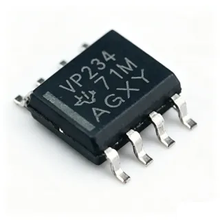
| パッケージ | SOIC-8 (D) |
| Number of Terminals | 8 |
| 実装タイプ | Surface Mount |
| 動作温度範囲 | 0 °C to 70 °C (commercial grade) |
| Terminal Form | Gull wing |
| Package Shape | Rectangular |
| RoHS Compliance | unknown - G4 ordering suffix denotes the lead-free/RoHS-compliant variant |
| Primary Application | ADSL central office and remote terminal line cards |
THS6072CD rectangular ピン配置ガイド
THS6072CD (rectangular パッケージ) のピン配置。 ピン番号、機能、接続図はメーカーのデータシートで定義されています。正確なフットプリントとはんだ付けのガイドラインについては、データシートを参照してください。

詳細なピン配置データはありません: THS6072CD.
詳細は データシート をご参照ください。
主な用途
THS6072CD の用途: 6 件s: ADSL Central Office Line Cards, ADSL Remote Terminal Units, ADSL Customer Premises Equipment with Splitters, Upstream and Downstream POTS/ADSL Transport Gear, Broadband Access Test and Measurement, Industrial Communication and Control Panels.
ADSL Central Office Line Cards
The THS6072CD suits central-office line cards where dozens of ADSL channels share a single power budget. Its 3.4 mA quiescent current per channel is roughly half that of competing ADSL receivers, so a 64-channel card using 32 dual devices draws only about 217 mA of receiver bias current, which directly shrinks the size of the card's supply and its thermal load. The 175 MHz -3 dB bandwidth gives margin above the ADSL downstream band, while 10 nV/√Hz input noise keeps the receiver contribution below the downstream ADC quantization floor. Place each receiver close to its line transformer and magnetics termination, and decouple locally so card-level switching converters do not inject differential noise into the input stage.
おすすめ
ADSL Remote Terminal Units
In remote terminal units, the THS6072CD delivers the analog receive path from the twisted pair down to the modem codec. Because the same rail powers the radio, DSP and line drivers, receiver power draw is a meaningful share of the thermal envelope; at 3.4 mA per channel the dual part contributes about 6.8 mA, freeing budget for DSP and transmit stages. The low 10 nV/√Hz voltage noise and -79 dBc distortion at 1 MHz minimize both in-band SNR loss and intermodulation products that would otherwise degrade upstream burst-mode decoding. Keep the differential input traces matched and short, and avoid adding gain ahead of the receiver, which would degrade the noise floor the part was designed to preserve.
おすすめ
ADSL Customer Premises Equipment with Splitters
The THS6072CD fits CPE designs that terminate both POTS and ADSL on the same pair, such as integrated splitter gateways. Its 175 MHz bandwidth comfortably passes the ADSL band while the low quiescent current keeps standby and always-on consumption low, which matters for CPE designs with strict power-consumption targets for home energy. The differential input structure naturally rejects the common-mode POTS voice-band energy that shares the line. Use it with a line filter and transformer network whose insertion loss is accounted for in the gain plan, and check that the receiver's supply sits where the datasheet allows, because supply noise on a low-noise receiver shows up directly as output noise.
おすすめ
Upstream and Downstream POTS/ADSL Transport Gear
Transport and aggregation equipment at the edge of the access network uses the THS6072CD where a differential receive stage must sit between line magnetics and a high-speed converter. The 175 MHz -3 dB bandwidth means one receiver can serve both upstream and downstream band requirements in a shared magnetics path, reducing the number of analog front-end channels per line. At 3.4 mA per channel the thermal design stays simple, and the low-noise input stage preserves headroom for downstream digital filtering. Keep the analog and digital return currents separated on the board so the switching returns of downstream converters do not share the receiver ground reference.
おすすめ
Broadband Access Test and Measurement
Test equipment that measures loop characteristics and receiver sensitivity benefits from a wideband, low-noise receive path, and the THS6072CD provides 175 MHz of bandwidth with a 10 nV/√Hz noise floor in a small 8-pin SOIC footprint. This leaves board area for instrumentation front ends and instrument-control interfaces. The wide bandwidth also allows the same receiver to observe harmonics and intermodulation products up to 1 MHz, and its -79 dBc distortion at 1 MHz is sufficient for loop-quality characterization. Provide a clean, low-impedance reference ground near the device and decouple the supply pins with short traces to keep measurement noise from dominating the result.
おすすめ
Industrial Communication and Control Panels
Industrial panels that combine legacy copper lines with digital field buses can use the THS6072CD as the analog receive front end for a legacy differential pair while modern data is handled by lower-speed transceivers. Its commercial 0 °C to 70 °C rating covers indoor panels, and the SOIC-8 footprint is easy to hand-assemble and rework. Because it is a receiver, the part does not need output drive current, so it can be powered from a modest 5 V-style rail shared with logic if the data sheet's supply range allows. Review the maximum supply voltage and total quiescent draw against your rail budget, and avoid placing the device adjacent to switching regulators without an LC filter on its supply pin.
おすすめ
おすすめ製品の概要
エンジニアリング参考データ: THS6072CD — 比較、設計ガイダンス、コンプライアンス情報。
選定ガイド
代替品との比較
| パラメータ | この製品 | THS6072 | THS6072ID | THS6072IDG4 | THS6072IDRG4 | THS6072CDG4 |
|---|---|---|---|---|---|---|
| Package | SOIC-8 (D) | SOIC-8 (D) - same | SOIC-8 (D) - same | SOIC-8 (D) - same | SOIC-8 (D) - same | SOIC-8 (D) - same |
| Brand | Texas Instruments | Texas Instruments | Texas Instruments | Texas Instruments | Texas Instruments | Texas Instruments |
| Device Type | Low-Power ADSL Differential Receiver | Low-Power ADSL Differential Receiver | Low-Power ADSL Differential Receiver | Low-Power ADSL Differential Receiver | Low-Power ADSL Differential Receiver | Low-Power ADSL Differential Receiver |
| Quiescent Current per Channel | 3.4 mA | 3.4 mA | 3.4 mA | 3.4 mA | 3.4 mA | 3.4 mA |
| Bandwidth (-3 dB) | 175 MHz | 175 MHz | 175 MHz | 175 MHz | 175 MHz | 175 MHz |
| Input Voltage Noise | 10 nV/√Hz | 10 nV/√Hz | 10 nV/√Hz | 10 nV/√Hz | 10 nV/√Hz | 10 nV/√Hz |
| Total Harmonic Distortion | -79 dBc at 1 MHz | -79 dBc at 1 MHz | -79 dBc at 1 MHz | -79 dBc at 1 MHz | -79 dBc at 1 MHz | -79 dBc at 1 MHz |
| Operating Temperature Range | 0 °C to 70 °C | 0 °C to 70 °C | -40 °C to 85 °C | -40 °C to 85 °C | -40 °C to 85 °C | 0 °C to 70 °C |
| RoHS / Lead-Free Marking | No G4 suffix on order code | No G4 suffix on order code | No G4 suffix on order code | G4 lead-free/RoHS marked | G4 lead-free/RoHS marked | G4 lead-free/RoHS marked |
主な差別化要因
- Half the quiescent power of other ADSL receivers, per channel (vs THS6072ID)
- Wide bandwidth headroom above the ADSL passband (vs THS6072IDG4)
- Commercial grade availability with an industrial-footprint sibling for rugged builds (vs THS6072IDRG4)
- Low noise floor combined with wide bandwidth in an 8-pin footprint (vs THS6072CDG4)
設計ノート
Treat the differential input path as a controlled-impedance pair. Route the two inputs with identical length, geometry, and reference plane so that common-mode noise and channel skew cancel in the receiver's differential stage. Terminate the line through the intended transformer or filter network directly at the input pins; every extra millimetre of trace adds parasitic inductance that interacts with the input capacitance and can degrade the 175 MHz response. Keep the analog ground reference for the receiver separate from the return currents of on-card switching converters by using a single-point or star connection at the supply entry.
The headline benefit of the THS6072CD is channel power density: at 3.4 mA per channel, a 64-channel ADSL line card consumes roughly 217 mA in receiver bias current, less than half of what competing ADSL receivers would draw. Use that budget headroom to specify local decoupling close to the supply pins rather than relying on bulk capacitance, and keep the supply rail itself clean. Because the input stage is low noise, supply ripple referenced through the device can dominate the noise floor, so an LC filter or separate regulator branch for the receiver section is justified on high-channel-count cards.
Do not place gain in front of the THS6072CD. The receiver is designed to present a low 10 nV/√Hz noise floor, and any pre-amplifier placed between the line and the receiver amplifies its own noise and adds distortion before the signal ever reaches the differential stage. A second common error is assuming the 175 MHz -3 dB figure applies to a closed-loop gain setting other than the datasheet condition; verify the gain and bandwidth combination in the typical performance curves before committing to a system bandwidth budget.
Because the receiver dissipates little power - roughly 6.8 mA of quiescent current across two channels at a typical 5 V-class supply - thermal design is rarely limiting for the device itself. It does matter at system level, because high channel counts concentrate heat into a small PCB area and raise the temperature of neighbouring magnetics and precision components. Space the SOIC-8 devices across the card rather than in a dense row, and check that the ambient rise does not push the receiver's case temperature above the 70 °C commercial limit of the CD grade; if it might, step up to the -40 °C to 85 °C THS6072ID ordering code.
コンプライアンス情報
The THS6072CD order code does not carry the TI 'G4' lead-free/RoHS suffix; lead-free G4 variants (THS6072CDG4, THS6072IDG4, THS6072IDRG4) exist in the same SOIC-8 (D) footprint and are the correct choice where RoHS-marked components are contractually required. AEC-Q100 does not apply to this commercial-grade communications interface IC.