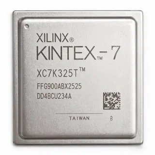
XC7K410T-1FFV900I Kintex-7 FPGA 900-BBGA | AMD Xilinx
部品番号: XC7K410T-1FFV900I ✓ 生産中XC7K410T-1FFV900I 概要
A field-programmable gate array is a semiconductor whose digital logic and interconnect can be configured after manufacture. Kintex-7 belongs to the FPGA hierarchy, combining programmable logic blocks, block RAM, digital signal processing resources, high-speed serial transceivers and programmable I/O. This combination allows complex parallel pipelines and high-speed interfaces to be implemented in one integrated device rather than across several fixed-function components.
The XC7K410T-1FFV900I provides 406,720 logic cells and 29,306,880 bits of total RAM according to the product listing. Its 500 ordinary user I/O support broad external connectivity, while 16 GTX serial lanes support high-speed serial links when the design, pin assignments, power architecture and device configuration are compatible. The -1 designation identifies the performance grade, while the I suffix identifies the industrial-temperature option.
The FFV900 package is a 900-ball FCBGA package, so PCB design must follow the AMD package pinout and escape-routing guidance rather than treating the device as a generic BGA. Power delivery, decoupling, GT transceiver connectivity and ball-map verification are central implementation concerns. Industrial deployments must also observe the device's operating-temperature and power-management requirements.
Typical applications include industrial automation, test and measurement, high-speed interface aggregation, communications infrastructure, video and image processing, and embedded control systems with substantial parallel logic. The device is appropriate when design flexibility, parallel processing capacity and serial connectivity are more important than the simplicity of a fixed-function ASIC.
Before schematic capture, verify the exact FFV900 ball assignments, voltage requirements, configuration pins, power rails and permitted I/O standards in the Kintex-7 package documentation. A drop-in candidate must match the same package and pin map exactly; speed-grade or package-suffix changes should not be assumed to preserve a completed board without engineering review.
This page combines the verified product listing, family-level FPGA specifications, practical design guidance, sourcing information and strict drop-in comparison criteria to support component selection and board-level implementation.
ドロップイン代替品: XC7K410T-1FFV900I — 同一パッケージでピン互換。PCBの作り直しが必要な異なるパッケージの部品は除外されています。
このシリーズのバリエーション
同一シリーズでドロップイン互換のモデル: XC7K410T-1FFV900I (同一形状・フットプリント) — 相違点: Block RAM, Logic Cells, Package, Process Technology, Speed Grade.
XC7K410T-1FFG900I
✅ ドロップイン価格はお問い合わせください
データシートを見る →XC7K410T-2FFG900I
✅ ドロップイン価格はお問い合わせください
データシートを見る →XC7K410T-2FF900I
✅ ドロップイン📋 参考代替品(カタログ未掲載)
XC7K410T-1FF900I
✅ ドロップイン価格はお問い合わせください
データシートを見る →XC7K410T-1FFG900C
✅ ドロップイン価格はお問い合わせください
データシートを見る →XC7K410T-L2FFG900I
✅ ドロップイン価格はお問い合わせください
データシートを見る →XC7K410T-1FFV900I 最大定格&電気的特性
| Device Type | Kintex-7 Field Programmable Gate Array (FPGA) |
| Logic Cells | 406,720 cells |
| Total RAM | 29,306,880 bits |
| Ordinary User I/O | 500 I/O |
| GTX Serial Lanes | 16 lanes |
| パッケージ | 900-BBGA, FCBGA |
| Package Dimensions | 31 x 31 mm |
| 実装タイプ | Surface Mount |
| Speed Grade | -1 |
| Temperature Grade | Industrial |
| Junction Temperature Range | -40 °C to +100 °C |
| Programmable Logic | Configurable FPGA logic and interconnect |
| Block RAM | 29,306,880 bits total RAM |
| Serial Interface | 16 GTX lanes |
| Device Family | Kintex-7 |
XC7K410T-1FFV900I 31 x 31 mm ピン配置ガイド
XC7K410T-1FFV900I (31 x 31 mm パッケージ) のピン配置。 このデジタルICには、GPIO、通信インターフェース (UART、SPI、I2C)、および電源ピンが含まれています。代替ピン機能と設定オプションについては、メーカーのデータシートを参照してください。組み込みシステム設計とPCBレイアウトに不可欠です。

詳細なピン配置データはありません: XC7K410T-1FFV900I.
詳細は データシート をご参照ください。
主な用途
XC7K410T-1FFV900I の用途: 6 件s: Industrial Automation Control, High-Speed Communications, Test and Measurement, Video and Image Processing, Aerospace and Defense Processing, Secure Network Infrastructure.
Industrial Automation Control
The XC7K410T-1FFV900I fits industrial automation systems that combine extensive parallel control logic with numerous field interfaces. Its 406,720 logic cells can host motion-control, sequencing, safety-interlock and machine-communication functions, while 500 ordinary user I/O provide substantial connectivity for sensors, actuators and discrete controls. The industrial-temperature designation and -40 °C to +100 °C junction range support designs intended for extended environmental operation. In implementation, engineers should partition I/O by voltage and bank constraints, verify the exact FFV900 ball map, and use the package pinout files before assigning external circuitry.
おすすめ
High-Speed Communications
The XC7K410T-1FFV900I is appropriate for communications aggregation, protocol conversion and high-speed data-processing systems because it combines 16 GTX serial lanes with a large programmable logic fabric. The 406,720 logic cells can implement framing, lane alignment, buffering and application-specific packet processing around the serial transceivers. Its 500 user I/O support parallel data paths and control interfaces. The design must still confirm each GTX lane's assigned package ball, supported protocol, reference-clock architecture, transceiver power rail and external termination before schematic completion.
おすすめ
Test and Measurement
The XC7K410T-1FFV900I suits test and measurement equipment requiring parallel acquisition, real-time processing, flexible control logic and multiple instrument interfaces. Its 406,720 logic cells and 29,306,880 bits of total RAM allow substantial buffering and digital signal-processing pipelines to be consolidated into one device. Sixteen GTX lanes can support high-speed data transfer when the selected FPGA configuration and package support the intended link standard. Practical implementation should address clock jitter, GT reference-clock routing, I/O standards, bank voltage compatibility and deterministic timing across the full industrial temperature range.
おすすめ
Video and Image Processing
The XC7K410T-1FFV900I can implement parallel video pipelines, pixel processing, frame buffering and image-format conversion because its 406,720 logic cells provide substantial configurable processing capacity. The 29,306,880 bits of total RAM support line buffers, frame storage or working memory depending on the selected architecture. Its 500 user I/O allow connection to sensors, capture devices and display-processing components when voltage and timing requirements align. Layout teams should plan high-speed memory and interface routing, control impedance, and separate analog-supply return paths to minimize data-converter or display noise coupling.
おすすめ
Aerospace and Defense Processing
The XC7K410T-1FFV900I can support programmable signal-processing and embedded-control tasks where logic density, I/O flexibility and industrial-grade operation are important. The 16 GTX lanes and 500 user I/O enable integration of acquisition, telemetry, control and auxiliary interfaces, while the programmable fabric permits algorithm updates without changing the PCB. Qualification for a specific aerospace program is separate from the industrial suffix. Engineers must review the exact radiation, screening, temperature, package and procurement requirements before treating this device as suitable for flight hardware.
おすすめ
Secure Network Infrastructure
The XC7K410T-1FFV900I is suitable for network infrastructure functions requiring parallel packet processing, deep control logic and flexible hardware acceleration. Its 406,720 logic cells can support packet classification, encryption pipelines, traffic management and test engines, while 16 GTX lanes provide high-speed backplane or line-card connectivity. The 500 ordinary user I/O can connect status, administration and lower-speed network interfaces. Designers must evaluate timing closure, memory bandwidth, power budget and transceiver configuration for the target traffic profile, while using secure boot and bitstream-protection features only after reviewing the applicable device documentation.
おすすめ
おすすめ製品の概要
エンジニアリング参考データ: XC7K410T-1FFV900I — 比較、設計ガイダンス、コンプライアンス情報。
選定ガイド
代替品との比較
| パラメータ | この製品 | XC7K410T-1FFG900I | XC7K410T-2FFG900I | XC7K410T-2FF900I | XC7K410T-1FF900I | XC7K410T-1FFG900C |
|---|---|---|---|---|---|---|
| Brand | AMD | AMD | AMD | AMD | AMD | AMD |
| Package | 900-BBGA, FCBGA | 900-BBGA, FCBGA | 900-BBGA, FCBGA | 900-BBGA, FCBGA | 900-BBGA, FCBGA | 900-BBGA, FCBGA |
| Logic Cells | 406,720 cells | 406,720 cells | 406,720 cells | 406,720 cells | 406,720 cells | 406,720 cells |
| Ordinary User I/O | 500 I/O | 500 I/O | 500 I/O | 500 I/O | 500 I/O | 500 I/O |
| GTX Serial Lanes | 16 lanes | 16 lanes | 16 lanes | 16 lanes | 16 lanes | 16 lanes |
| Speed Grade | -1 | -1 | -2 | -2 | -1 | -1 |
| Package Pin Compatibility | FFV900 ball map | FFG900 suffix; exact ball-map confirmation required | FFG900 suffix; exact ball-map confirmation required | FF900 suffix; exact ball-map confirmation required | FF900 suffix; exact ball-map confirmation required | FFG900 suffix; exact ball-map confirmation required |
主な差別化要因
- Full industrial-grade resource configuration (vs XC7K410T-1FFG900C)
- Lower speed grade than the -2 alternatives (vs XC7K410T-2FFG900I)
- Large programmable logic and memory combination (vs XC7K410T-1FFG900I)
- Same-family 16-lane GTX connectivity (vs XC7K410T-2FF900I)
設計ノート
Start the layout from the exact FFV900 package drawing and official ball map, not from a generic 900-BBGA template. Verify every power, ground, configuration, clock and user-I/O assignment against the package pinout files. Preserve the documented ball-pad geometry, solder-mask definition and component placement rules, and perform a manufacturing stack-up review before releasing the PCB.
Plan separate, low-impedance distribution for core, I/O and transceiver supplies. Place local decoupling close to the appropriate device balls and follow the AMD decoupling recommendations in the Kintex-7 power guidance. Estimated: supply-current and voltage values must be taken from the selected configuration and operating corner; multiply each rail's calculated current by its supply voltage to obtain rail power, then include conversion and distribution losses in the system thermal budget.
Treat GTX and high-speed user-I/O routes as controlled-impedance interconnects. Use the package pinout and transceiver documentation to confirm legal lane assignments, reference-clock pins, external component placement and insertion-loss requirements. Avoid routing high-speed signals through split planes, and validate the complete stack-up with simulation before fabrication because the 31 x 31 mm FCBGA package limits escape-routing flexibility.
Do not infer equivalence from matching logic-cell counts or the 900-BBGA package name alone. FFV900, FF900, FFG900 and L2 designations can represent different package, speed, power or temperature options. Before substitution, compare the exact ordering code, package drawing, ball map, supported I/O standards, configuration method, power rails, timing grade and required qualification status.
コンプライアンス情報
The verified listings identify the product, package and industrial-temperature classification but do not provide explicit RoHS, REACH, lead-free, halogen-free or conflict-minerals declarations. AEC-Q100 is not an appropriate qualification category for this FPGA.