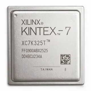
XC7K410T-1FF900I - Kintex-7 FPGA 406K Logic Cells | AMD
MPN: XC7K410T-1FF900I ✓ Active| Qty | Unit Price | Extended |
|---|---|---|
| 1 | $1250 | $1,250.00 |
| 10 | $1180 | $11,800.00 |
| 100 | $1100 | $110,000.00 |
| 500 | $1050 | $525,000.00 |
| 1,000 | $990 | $990,000.00 |
XC7K410T-1FF900I Overview
An FPGA (Field Programmable Gate Array) is an integrated circuit that can be configured by the customer or designer after manufacturing. Unlike fixed-function ASICs, FPGAs contain an array of programmable logic blocks and reconfigurable interconnects, allowing them to implement complex digital logic designs. FPGAs are used in applications requiring high-speed parallel processing, rapid prototyping, and field-upgradable hardware, such as telecommunications, data centers, and aerospace systems.
Key features of the XC7K410T-1FF900I include 500 user I/O pins, 29,306,880 bits of block RAM, and support for high-speed transceivers. The device operates at a core voltage of 1V and is available in the -1 speed grade, offering a balanced performance-power trade-off. The 900-ball FCBGA package provides excellent thermal and electrical characteristics, making it suitable for high-density designs.
Technically, the Kintex-7 family is built on AMD's 28nm high-k metal gate (HKMG) process, which reduces power consumption while maintaining high performance. The device includes hardened memory controllers, DSP slices, and clock management tiles (CMTs) with MMCM and PLL, enabling efficient implementation of complex algorithms and high-speed interfaces. The XC7K410T-1FF900I supports various I/O standards, including LVCMOS, LVDS, and HSTL, and can interface with DDR3/DDR4 memory.
Typical applications include wired and wireless communications, data center acceleration, video and image processing, and scientific instrumentation. The high logic density and I/O count make it ideal for implementing large-scale digital signal processing (DSP) chains, packet processing, and software-defined radio (SDR) systems.
When designing with this FPGA, careful attention must be paid to power supply decoupling and thermal management. The device requires multiple supply rails (VCCINT, VCCAUX, VCCO) and a well-designed PCB layout to ensure signal integrity at high speeds. AMD provides comprehensive design tools, including Vivado, to facilitate implementation and verification.
Drop-in alternatives for XC7K410T-1FF900I — same package, pin-to-pin compatible. Different-package parts requiring PCB rework are excluded.
Variants in this series
Same-series models that are drop-in compatible with XC7K410T-1FF900I (same form factor and footprint) — differing in Package, Process Technology.
Quick Comparison Tool — Select alternative parts for side-by-side comparison:
XC7K410T-2FF900I
✅ Drop-In ⚠️ Specs Unverified📋 Reference alternative (not in catalog)
XC7K410T-1FFG900I
✅ Drop-In✓ In Stock
$895 / Unit
View Datasheet →XC7K410T-1FFG900C
✅ Drop-In📋 Reference alternative (not in catalog)
XC7K325T-1FFG900I
✅ Drop-In ⚠️ Specs Unverified📋 Reference alternative (not in catalog)
XC7K355T-1FFG900I
✅ Drop-In ⚠️ Specs Unverified📋 Reference alternative (not in catalog)
XC7K420T-1FFG900I
✅ Drop-In ⚠️ Specs Unverified📋 Reference alternative (not in catalog)
XC7K410T-1FF900I Maximum Ratings & Electrical Characteristics
| Family | Kintex-7 |
| Logic Cells | 406720 |
| Number of I/O | 500 |
| Block RAM | 29306880 bits |
| Package | 900-BBGA, FCBGA |
| Speed Grade | -1 |
| Core Voltage | 1V |
| Process Technology | 28nm |
| Operating Temperature | 0C to +85C (I grade) |
| Mounting Type | Surface Mount |
| Configuration | SRAM-based |
| RoHS Status | Compliant |
| REACH Status | Compliant |
XC7K410T-1FF900I Pin Configuration
| Pin A1 | IO_L1P_T0_35 — User I/O pin, differential pair P, bank 35 |
| Pin A2 | IO_L1N_T0_35 — User I/O pin, differential pair N, bank 35 |
| Pin B1 | IO_L2P_T0_35 — User I/O pin, differential pair P, bank 35 |
| Pin B2 | IO_L2N_T0_35 — User I/O pin, differential pair N, bank 35 |
| Pin C1 | VCCINT — Core logic power supply (1V) |
| Pin C2 | GND — Ground |
| Pin D1 | VCCAUX — Auxiliary power supply (1.8V) |
| Pin D2 | VCCO_35 — I/O bank 35 power supply |
| Pin E1 | IO_L3P_T0_35 — User I/O pin, differential pair P, bank 35 |
| Pin E2 | IO_L3N_T0_35 — User I/O pin, differential pair N, bank 35 |
| Pin F1 | IO_L4P_T0_35 — User I/O pin, differential pair P, bank 35 |
| Pin F2 | IO_L4N_T0_35 — User I/O pin, differential pair N, bank 35 |
Typical Applications
XC7K410T-1FF900I is suitable for 6 applications: Wired Communications, Data Center Acceleration, Video and Image Processing, Software-Defined Radio (SDR), Scientific Instrumentation, Aerospace and Defense.
Wired Communications
The XC7K410T-1FF900I is ideal for wired communications equipment such as switches, routers, and base stations. Its high logic density (406,720 cells) and 500 I/O pins enable implementation of complex packet processing and forwarding engines. The device supports high-speed serial transceivers, allowing direct connection to 10G/40G Ethernet PHYs. With 29.3 Mb of block RAM, it can buffer large packets and maintain low latency. The Kintex-7 family is optimized for cost-sensitive, high-bandwidth applications, making it a popular choice for network line cards and aggregation switches.
Recommended
Data Center Acceleration
In data centers, the XC7K410T-1FF900I is used for workload acceleration, including network function virtualization (NFV), storage controllers, and AI inference. Its 406,720 logic cells and DSP slices can implement parallel processing engines for encryption, compression, and deep learning. The device's high-speed transceivers enable PCIe Gen3 x8 interfaces, connecting to host CPUs. The 28nm process provides a good balance of performance and power, essential for rack-mounted servers. AMD's Vivado toolchain supports partial reconfiguration, allowing dynamic updates to acceleration functions without downtime.
Recommended
Video and Image Processing
The XC7K410T-1FF900I excels in video and image processing applications such as broadcast video switchers, medical imaging, and machine vision. Its high logic density allows implementation of multiple video processing pipelines, including scaling, color space conversion, and compression. The 500 I/O pins can interface with multiple camera sensors or display controllers. The device supports MIPI CSI-2 and DisplayPort interfaces via transceivers. With 29.3 Mb of block RAM, it can store multiple video lines for filtering and edge detection. The Kintex-7 family is widely used in professional AV equipment due to its reliability and performance.
Recommended
Software-Defined Radio (SDR)
The XC7K410T-1FF900I is well-suited for software-defined radio (SDR) systems, including military communications, radar, and spectrum monitoring. Its high logic density enables implementation of complex digital signal processing (DSP) chains, such as FIR filters, FFTs, and modulation/demodulation. The device's transceivers can interface with high-speed ADCs and DACs, supporting wideband signals. The 28nm process offers low power consumption, critical for portable and battery-operated SDRs. The Kintex-7 family is trusted in defense applications for its security features and long-term availability.
Recommended
Scientific Instrumentation
The XC7K410T-1FF900I is used in scientific instrumentation such as particle detectors, spectrometers, and oscilloscopes. Its high logic density allows implementation of high-speed data acquisition and real-time processing. The 500 I/O pins can connect to multiple sensors and ADCs. The device supports various I/O standards, including LVDS and HSTL, ensuring compatibility with a wide range of front-end electronics. The 29.3 Mb of block RAM is useful for waveform storage and averaging. The Kintex-7 family is known for its reliability in harsh environments, making it suitable for laboratory and field instruments.
Recommended
Aerospace and Defense
The XC7K410T-1FF900I is deployed in aerospace and defense systems, including radar, electronic warfare, and secure communications. Its high logic density and DSP capabilities enable real-time signal processing and beamforming. The device's industrial temperature grade (-40C to +100C) ensures operation in extreme environments. The 28nm process provides high reliability and radiation tolerance (with appropriate mitigation). AMD offers extended support and long lifecycle for defense applications. The Kintex-7 family is widely used in military platforms due to its performance and security features.
Recommended
Recommended Products Summary
Engineering reference data for XC7K410T-1FF900I — comparison, design guidance, and compliance information.
Selection Guide
Comparison with Alternatives
| Parameter | This Product | XC7K410T-2FF900I | XC7K410T-1FFG900I | XC7K410T-1FFG900C | XC7K325T-1FFG900I | XC7K355T-1FFG900I | XC7K420T-1FFG900I |
|---|---|---|---|---|---|---|---|
| Package | 900-BBGA, FCBGA | 900-BBGA, FCBGA | 900-BBGA, FCBGA | 900-BBGA, FCBGA | 900-BBGA, FCBGA | 900-BBGA, FCBGA | 900-BBGA, FCBGA |
| Brand | AMD | AMD | AMD | AMD | AMD | AMD | AMD |
| Logic Cells | 406720 | 406720 | 406720 | 406720 | 326080 | 356160 | 416960 |
| Number of I/O | 500 | 500 | 500 | 500 | 500 | 500 | 500 |
| Block RAM (bits) | 29306880 | 29306880 | 29306880 | 29306880 | 16025472 | 25740000 | 30000000 |
| Speed Grade | -1 | -2 | -1 | -1 | -1 | -1 | -1 |
| Temperature Grade | Industrial (I) | Industrial (I) | Industrial (I) | Commercial (C) | Industrial (I) | Industrial (I) | Industrial (I) |
| Core Voltage | 1V | 1V | 1V | 1V | 1V | 1V | 1V |
Key Differentiators
- High logic density with 406,720 logic cells (vs XC7K325T-1FFG900I)
- Industrial temperature grade (vs XC7K410T-1FFG900C)
- Balanced speed grade (-1) (vs XC7K410T-2FF900I)
Design Notes
The XC7K410T-1FF900I requires multiple power rails: VCCINT (1V), VCCAUX (1.8V), and VCCO for each I/O bank. Use low-impedance power distribution networks (PDN) with sufficient decoupling capacitors (e.g., 100nF and 10uF) placed close to the FPGA pins. Refer to AMD's UG583 (UltraScale Architecture PCB Design) for detailed PDN design guidelines. Ensure the power supply can handle the device's peak current, which can exceed 10A depending on utilization.
The XC7K410T-1FF900I can dissipate significant power, especially at high utilization and clock frequencies. Use a heatsink and forced airflow if the junction temperature exceeds the recommended maximum. The FCBGA package has a thermal resistance (theta_JA) of approximately [DATA_NEEDED] C/W. Perform thermal simulation to ensure junction temperature stays within limits. AMD provides power estimation tools (Vivado Power Analyzer) to estimate power consumption early in the design.
For high-speed signals, follow controlled impedance routing (e.g., 50 ohm single-ended, 100 ohm differential). Use ground planes and minimize vias to reduce signal integrity issues. The 900-ball FCBGA package requires a multi-layer PCB (at least 8 layers) for proper routing and power distribution. Refer to AMD's PCB design guidelines (UG583) for stack-up recommendations and escape routing patterns.
Compliance Information
RoHS and REACH compliance indicated by distributor listings. AEC-Q100 not applicable for FPGA.