DC-DC 컨버터
제품 (764)

TPSM33615FRDNR - 36V 1.5A Sync Buck Module | Texas Instruments
The Texas Instruments TPSM33615FRDNR is a 3-V to 36-V input, 1-V to 15-V output, 1.5-A synchronous buck power module integrated in a HotRod QFN-FCMOD (RDN) package with 11 pins. Headline parameters include 36-V maximum input voltage, 1.5-A continuous load current, and 88% typical efficiency, all delivered in a 3.5 mm x 4.5 mm surface-mount footprint. A buck converter (step-down switching regulator) is a switching-converter topology that reduces a higher DC input voltage to a lower regulated DC output voltage using an inductor, capacitor, and synchronous MOSFET switches. It sits within the broader power management IC hierarchy: buck converter -> DC-DC converter -> switching regulator -> power management IC. A power module such as the TPSM33615FRDNR integrates the controller, MOSFETs, inductor, and compensation network into one package, simplifying PCB layout and reducing design risk versus discrete buck implementations. Key features include 1.5-uA quiescent current, 1-MHz fixed switching frequency, programmable output voltage from 1 V to 15 V, and selectable PFM or FPWM light-load operation. The HotRod QFN-FCMOD package reduces parasitic inductance and improves thermal performance. Integrated protections include over-current, over-temperature, under-voltage lockout, automatic fault recovery, and 1% output voltage accuracy across load and line. The integrated inductor and shielding minimize radiated EMI, which is critical for industrial and instrumentation applications that must pass CISPR 25 or CISPR 32. Technically, the TPSM33615FRDNR uses a peak current-mode control topology with internal compensation, an external RT resistor to program switching frequency, and a MODE pin to select PFM (light-load efficiency) versus FPWM (constant-frequency low-noise) behavior. The HotRod flip-chip QFN package eliminates bond wires, reducing switching-node ringing and DC resistance losses. Typical applications include industrial 24-V rail point-of-load regulation, factory automation sensors, building automation controllers, low-noise bias supplies for analog front ends, and portable or battery-powered equipment operating from multi-cell lithium packs. The wide 3-V to 36-V input range supports 12-V and 24-V industrial buses directly. When designing with this device, keep the input capacitors close to VIN and PGND pins to minimize switching-node ringing, and connect the exposed thermal pad to a sufficient ground copper pour. Select PFM mode for highest light-load efficiency, or FPWM when low EMI is the top priority. This page synthesizes distributor pricing, drop-in alternatives, design notes, and application guidance not found in the manufacturer datasheet alone, giving engineers a single reference for component selection, PCB implementation, and sourcing decisions.

TPSM53604RDAR - 36V 4A Step-Down Power Module | TI
The Texas Instruments TPSM53604RDAR is a 36-V input, 4-A step-down DC/DC power module that integrates power MOSFETs, a shielded inductor, and passives in a thermally enhanced 15-pin Enhanced HotRod QFN package measuring 5.5 mm x 5 mm x 4 mm, delivering an adjustable 1 V to 7 V output from a 3.8 V to 36 V input. A power module is a highly integrated point-of-load (PoL) DC/DC converter: within the broader hierarchy of power management ICs, a step-down (buck) converter reduces a higher input voltage to a lower regulated output, and a power module goes one step further by co-packaging the controller or converter IC, switching MOSFETs, inductor, and key passives into a single surface-mount package. This integration eliminates inductor selection and magnetics design from the engineering workflow, dramatically reducing board area, bill-of-materials count, and design risk compared with a discrete buck converter solution. Key features of the TPSM53604 include its wide 3.8 V to 36 V input range, which directly supports 12-V, 24-V, and industrial 24 V nominal rails with transient headroom; an adjustable output spanning 1 V to 7 V; a continuous 4-A output current rating; and a fixed-frequency peak-current-mode control topology with optimized internal compensation. The Enhanced HotRod QFN construction places the die close to the package pins, minimizing parasitic inductance for low EMI and improved thermal performance. Technically, the module integrates a shielded inductor that produces low radiated electromagnetic emissions, simplifying CISPR-class EMI compliance work. The thermally enhanced package dissipates heat through the PCB, and the simple footprint with all pins on the perimeter makes layout and inspection straightforward. Shutdown quiescent operation and enable functionality support low standby power designs. Typical applications include industrial automation and PLC I/O modules, 12-V and 24-V distributed power systems, test and measurement instrumentation, telecom and networking equipment auxiliary rails, and embedded processor point-of-load supplies derived from wide-input industrial buses. Design consideration: at high input voltages and high output current, verify junction temperature using the datasheet thermal derating curves; adequate PCB copper area beneath the module is the primary thermal solution. This page synthesizes verified distributor data, same-family drop-in alternatives, and practical design guidance not found in the manufacturer datasheet alone. Pricing shown reflects distributor data as of 2026-10-19.
TPSM5601R5 - 60V In, 1.5A Step-Down Power Module | TI
The Texas Instruments TPSM5601R5 is a highly integrated 1.5-A step-down DC/DC power module combining a 60-V maximum input converter, power MOSFETs, a shielded inductor, and support passives in a thermally enhanced 5-mm x 5.5-mm x 4-mm 15-pin Enhanced HotRod QFN package. It delivers an adjustable output voltage of 1.0 V to 6 V from a 4.2-V to 60-V input range with a fixed 400-kHz switching frequency. A power module is a complete DC-DC converter solution that integrates the controller, switching MOSFETs, inductor, and compensation network into a single surface-mount package. Within the power management hierarchy (power module -> step-down converter -> DC-DC converter -> power management IC), modules eliminate magnetics selection and loop compensation design, reducing time-to-market and layout risk compared to discrete converter solutions. Key features include the wide 60-V input rating suited to 24-V and 48-V industrial rails with transient headroom, an output range of 1.0 V to 6 V set by a single external resistor divider, and as few as four external components for the complete solution. The Enhanced HotRod QFN construction places the die directly against the thermal pad, delivering low EMI, excellent thermal performance, and all pins accessible from the package perimeter for simple layout and inspection. The internal compensation and integrated shielded inductor provide stable operation across the load range while reducing solution height and BOM count. The device operates from a -40C to +125C junction temperature range, supporting industrial and automotive-adjacent environments. The TPSM5601R5S variant adds spread-spectrum operation for lower EMI peaks, and the TPSM5601R5H variant extends output capability up to 16 V. Typical applications include 24-V and 48-V industrial bus power supplies, factory automation and PLC I/O modules, test and measurement point-of-load rails, and distributed power systems that need a compact, regulated 1-V to 6-V rail from a wide input. Design tip: because the inductor is integrated, thermal design centers on the PCB copper pour under the thermal pad - provide at least a 1-square-inch ground plane with thermal vias for reliable operation at full 1.5-A load at elevated ambient temperatures.
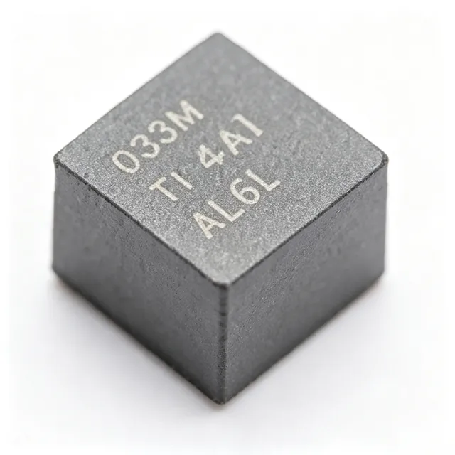
TPSM81033VCDR - 2A 2.4MHz Synchronous Boost Module | TI
The Texas Instruments TPSM81033VCDR is a 5.5V, 2A synchronous boost power module using TI MagPack packaging technology, integrating a 0.43uH power inductor, power MOSFETs, and control circuitry into a 2.6mm x 2.5mm QFN-FCMOD (9) package. It accepts 1.8V to 5.5V input and delivers a 2.2V to 5.5V output with a 2A typical valley switching current limit. A boost converter (step-up switching regulator) is a DC-DC converter that raises an input voltage to a higher regulated output by storing energy in an inductor and releasing it at higher voltage through a switching FET. Boost converters form part of the power management IC hierarchy and are essential wherever battery voltage is lower than the load rail, such as single-cell Li-ion or alkaline systems needing a 5V rail. Key features include the integrated inductor enabled by MagPack technology, 2.4MHz switching frequency that allows tiny external components and fast transient response, fixed 5.0V output option by connecting FB to AVIN, selectable light-load mode (auto PFM or forced PWM) via the MODE pin, and power-good output. Protection features include 5.75V output overvoltage protection, output short-circuit protection, and thermal shutdown. The device uses adaptive constant on-time valley-current-control topology, providing fast load transients and predictable behavior. Forced PWM mode trades light-load efficiency for constant switching frequency, important for noise-sensitive RF and analog rails. Typical applications include smart devices and portable battery-powered equipment, RF power amplifiers needing a stable 5V from Li-ion cells, and OLED or display bias supplies. The tiny footprint and minimum external component count make it ideal for space-constrained wearables and IoT devices. Design consideration: boost converter output current capability decreases as input voltage drops; verify the 2A valley current limit supports your load at minimum VIN, and follow the datasheet PCB layout for thermal performance of the exposed package.
TPSM81033VCDR - 2A, 2.4MHz Boost Power Module | TI
The Texas Instruments TPSM81033VCDR is a 5.5V, 2A, 2.4MHz synchronous boost power module using MagPack packaging technology. It integrates a 0.43uH power inductor, power switches, and control circuitry into a compact 2.6mm x 2.5mm QFN-FCMOD (9) package, providing a nearly complete DC-DC boost converter solution with a minimum of external components. A power module is a type of DC-DC converter that integrates the power inductor and MOSFETs of a switching regulator into a single surface-mount package, sitting within the broader hierarchy of power management ICs that also includes LDOs, buck converters, and controllers. By integrating magnetics, modules dramatically reduce solution size and simplify layout compared to discrete converter designs. Key features include a 1.8V to 5.5V input voltage range, an adjustable 2.2V to 5.5V output voltage range (with fixed 5.0V output when FB is connected to AVIN), a 2A valley switching current limit, and integrated 0.43uH power inductor with excellent thermal performance. The device operates at 2.4MHz switching frequency using an adaptive constant on-time valley-current-control topology, enabling small external components and fast transient response. The module offers two light-load modes selected via the MODE pin: automatic PFM mode for highest efficiency and forced PWM mode for fixed-frequency noise immunity. Protection features include 5.75V output overvoltage protection, output short-circuit protection, and thermal shutdown. A power good output supports power-rail monitoring and sequencing. Typical applications include battery-powered smart devices, portable equipment, Li-ion cell to 5V conversion, and point-of-load boost rails in compact electronics where board space is constrained. The small 2.6mm x 2.5mm footprint suits wearables and handheld instrumentation. Design consideration: because the current limit is a valley limit of 2A typical, verify peak inductor current under worst-case load, minimum input voltage, and maximum output power to avoid hitting current limit during load transients.
TPSM81033VCDR - 5.5V 2A Boost Power Module | Texas Instruments
The Texas Instruments TPSM81033VCDR is a 5.5V, 2A synchronous boost power module with MagPack packaging technology, integrating a 0.43uH power inductor and power MOSFETs in a compact 2.6mm x 2.5mm QFN-FCMOD (9) package. It operates from a 1.8V to 5.5V input and delivers an adjustable 2.2V to 5.5V output, with a fixed 5.0V option by connecting FB to AVIN. A boost converter is a DC-DC switching regulator that steps an input voltage up to a higher output voltage. It is essential in battery-powered systems where cell voltage falls below the required rail. The TPSM81033 belongs to the power module family within power management ICs, integrating the magnetic component and power stage to reduce design effort and board space versus discrete solutions. Key features include a 2A valley switching current limit, fixed 2.4MHz switching frequency for small external components and low ripple, and an integrated 0.43uH inductor with excellent thermal performance. Adaptive constant on-time valley-current-control topology regulates the output, while two light-load modes (auto PFM and forced PWM) selected via the MODE pin balance efficiency and noise immunity. Optional spread spectrum frequency modulation minimizes EMI. The synchronous rectifier architecture eliminates the external Schottky diode, improving efficiency, and the integrated inductor reduces parasitic losses and radiated EMI. Only input and output capacitors plus feedback resistors are required. Protection features include 5.75V output overvoltage protection, output short-circuit protection, thermal shutdown, and a power good output for sequencing in multi-rail systems. Typical applications include smart devices and portable equipment powered by batteries, IoT sensor power supplies, and TFT-LCD bias or OLED display rails. The wide input range and high switching frequency suit space-constrained designs. Design tip: ensure adequate input and output capacitance for stability and low ripple, and use the MODE pin to trade efficiency against noise. For a fixed 5V output, tie FB to AVIN per the datasheet layout guidelines.
TPSM82813 - 3A 6V Step-Down Power Module | TI
The Texas Instruments TPSM82813 is a synchronous step-down DC/DC power module with integrated inductor, delivering up to 3A output current from a 2.75V to 6V input supply. Available in QFN and MagPack (SIL) packages, output voltage is adjustable from 0.6V to 5.5V via external resistors. A step-down (buck) converter is a DC/DC power converter that efficiently reduces a higher input voltage to a lower regulated output. Power modules integrate the inductor and control circuitry into a single package, sitting one level above discrete buck converters in the power management IC hierarchy and dramatically reducing design effort and PCB area compared to controller-plus-inductor solutions. Key features include optional frequency synchronization, adjustable soft-start, and output voltage tracking for power sequencing. The device also offers spread spectrum for EMI reduction, a power good output, adjustable UVLO, and light-load efficiency mode. Efficiency reaches approximately 95%, minimizing losses in high-current point-of-load designs. Technically, the TPSM82813 uses a fixed-frequency peak current-mode control topology, providing fast transient response and stable loop behavior. The integrated inductor is optimized for low loss and contained EMI, while the MagPack package improves thermal performance. Thermal behavior is characterized on a JEDEC 51-7 defined PCB. Typical applications include point-of-load converters for FPGAs, DSPs, and ASICs, plus power supplies for telecommunication, test and measurement, medical, and industrial sensor equipment. The wide 2.75V-6V input supports 5V and 3.3V bus conversions, and the small footprint enables dense rail designs. Design tip: follow datasheet input/output capacitance recommendations, configure soft-start and tracking for your power-up sequence, and use thermal vias under the module per the recommended land pattern. Pricing as of 2026-08-30, see tiers below.
TPSM82816 - 6A Step-Down Power Module 2.7-6V | TI
The Texas Instruments TPSM82816 is a 2.7V to 6V input, 6A output synchronous step-down DC/DC power module with an integrated inductor, packaged in the compact MicroSiP (SIE) package. It belongs to the TPSM8281x family of pin-to-pin 1A, 2A, 3A, 4A, and 6A compatible modules, delivering high power density and ease of use for point-of-load (PoL) power supplies. A step-down power module is a complete DC/DC converter solution that combines the switching regulator, power MOSFETs, and magnetic components in a single package. Unlike discrete regulators that require separate inductor selection and layout optimization, power modules simplify design, shrink solution size, and reduce EMI and efficiency risk. Power modules sit within the power management IC hierarchy, bridging discrete converters and fully integrated PMICs. Key features include an adjustable output voltage from 0.6V to 5.5V via a single resistor divider, optional frequency synchronization to an external clock, adjustable soft-start, and output voltage tracking for rail sequencing. Peak efficiency exceeds 90% for typical 5V-to-1.8V conversions, with the shielded integrated inductor improving EMI behavior. The device is based on a fixed-frequency peak current-mode control topology, which provides fast transient response and stable operation with ceramic output capacitors. The package integrates everything needed for a minimal-footprint POL supply, and protection features include overcurrent, overvoltage, and thermal shutdown. The switching frequency can be programmed to trade efficiency against solution size. Typical applications include POL power for FPGAs, ASICs, and processors in telecommunication, test and measurement, medical, and industrial systems, where TI cites high power density and ease of use as primary benefits. Because the family is pin-to-pin compatible, a single PCB layout supports current tiers from 1A to 6A, simplifying BOM scaling across product variants. When designing with the TPSM82816, provide adequate input and output ceramic capacitance for stability and transient response, and use the SS/TRACK pin to sequence multiple rails in multi-voltage systems.
TPSM82822A - 2A Step-Down Module, Integrated Inductor | TI
The Texas Instruments TPSM82822A is a 5.5-V input, 2-A synchronous step-down converter power module with an integrated inductor and forced PWM mode, housed in a compact 2 x 2.5 x 1.1 mm MicroSiP (uSiP) package. It delivers an adjustable output from 0.6 V to 4 V, simplifying point-of-load power design. A step-down converter, or buck converter, is a switching voltage regulator that efficiently reduces a higher DC input voltage to a lower regulated output. Within the power management IC hierarchy, the TPSM82822A is a power module: it integrates the buck converter IC, power MOSFETs, and the magnetic inductor into one surface-mount package, collapsing an entire DC-DC solution into about 5 mm2 of board area. Key features include a 2.4 V to 5.5 V input range, 2 A continuous output current, forced PWM operation for constant 2.2 MHz switching frequency and predictable EMI, power-good output, enable pin, and internal soft-start. Efficiency reaches approximately 95% at typical loads, and the high operating frequency allows small external capacitors and low output ripple. Technically, the module uses a synchronous buck architecture with integrated low-DS(on) MOSFETs and a proprietary control scheme. Integrating the inductor inside the package minimizes parasitic loop inductance, reduces radiated EMI, and enables automated assembly with standard surface-mount equipment per the TPSM8282x datasheet. Typical applications include powering FPGAs, DSPs, ASICs, and MCUs in industrial systems, optical modules, solid-state drives, and portable devices where board space is at a premium. Forced PWM keeps output ripple low and constant-frequency, suiting noise-sensitive analog and RF rails. Design consideration: follow the datasheet input/output capacitor recommendations exactly for stability, and provide adequate thermal copper area for sustained 2 A loads; the module does not eliminate thermal design entirely.
TPSM828303 - 3A Low-EMI Buck Module 2.25-5.5V | Texas Instruments
The Texas Instruments TPSM828303 is a 3A synchronous step-down DC/DC power module with integrated inductor, operating from a 2.25V to 5.5V input and providing an adjustable output from 0.5V to 4.5V in a compact QFN (RDS) or MagPack (PVC) package. A DC/DC power module is a complete point-of-load power supply that integrates the controller, power MOSFETs, inductor, and compensation into a single surface-mount package. As a member of the buck (step-down) converter family within the broader power management IC hierarchy, it efficiently reduces a higher input voltage to a lower output voltage while minimizing external component count, layout effort, and design risk compared to discrete converter solutions. Key features include the DCS-Control topology for fast load transient response with small output capacitance, 1% feedback voltage accuracy over the full operating range, and integrated EMI reduction technologies that ease radiated emissions compliance. Automatic PWM/PFM transition maximizes light-load efficiency, and enable, power good, output discharge, and overcurrent protection functions simplify system integration. The TPSM828303 is pin-to-pin compatible with the 1A (TPSM828301) and 2A (TPSM828302) family members, enabling current-rating scalability on one PCB layout. The integrated inductor with MagPack magnetic shielding (TPSM828303APVCBR variant) reduces radiated EMI and board area versus discrete designs. Operation over a -40C to +125C junction range suits industrial environments. Typical applications include point-of-load (POL) power for FPGAs, DSPs, and ASICs, optical module supplies, test and measurement equipment, and noise-sensitive portable designs where low EMI is mandatory. Design tip: follow the datasheet input/output capacitance recommendations - the DCS-Control topology supports output capacitors up to 200uF, and the EN pin plus power good signal enable proper rail sequencing in multi-rail systems. Prices as of 2026-08-30.
TPSM82866A - 6A Step-Down Power Module | Texas Instruments
The Texas Instruments TPSM82866A is a 6A step-down power module with an integrated inductor, operating from a 2.4V to 5.5V input and providing an adjustable output from 0.6V to 5.5V. It comes in a 3.5mm x 4.0mm thin overmolded QFN package (RDJ), integrating a synchronous buck converter and shielded inductor for a compact point-of-load solution. A step-down power module is a complete DC-DC converter solution that integrates the controller, power FETs, and inductor into a single package. Belonging to the power management IC family of non-isolated point-of-load (PoL) converters, such modules reduce design complexity, minimize PCB area, and improve thermal performance compared to discrete buck converter designs, which is essential for powering modern digital loads. Key features include 6A continuous output current, high efficiency, and DCS-Control topology for fast transient response and stable operation. The integrated 220nH shielded inductor (±20% tolerance in RDJ/RDM packages) provides excellent EMI performance. The module offers power-good output, enable pin, and adjustable switching frequency for flexible power sequencing and design optimization. Technically, the TPSM8286xA family uses the DCS-Control (Direct Control with Seamless transition into energy saving mode) architecture, delivering fixed-frequency operation with excellent load and line regulation. The TPSM82864A and TPSM82866A in RDJ and RDM packages are pin-to-pin and BOM-to-BOM compatible, allowing a 4A option on the same footprint. The TPSM8286xAA0HRDMR variants provide higher efficiency due to increased package height, and the RCF MagPack variant uses a 200nH inductor with enhanced EMI shielding. Typical applications include core power supplies for FPGAs, CPUs, and ASICs, optical modules, and medical and industrial equipment, where board space is at a premium and high current density is required. When designing with this module, ensure adequate input and output capacitance for stability. The integrated inductor simplifies layout, but proper grounding and thermal vias remain essential for optimal thermal performance at full 6A load.
TPSM82866C - 6A Step-Down Power Module I2C | Texas Instruments
The Texas Instruments TPSM82866C is a 6A step-down power module with an integrated inductor and I2C interface, designed for compact, high-density power delivery. It operates from a 2.4V to 5.5V input and provides an adjustable output voltage, making it suitable for a wide range of point-of-load (PoL) applications. The module is housed in a MagPack (RCF) QFN package measuring only 2.3mm x 3mm, achieving a power density of nearly 1A per 1mm2 of area. A step-down power module is a complete DC-DC converter that integrates the controller, power FETs, inductor, and compensation into a single package. This integration simplifies design, reduces external component count, and minimizes PCB footprint compared to discrete buck regulator solutions. The TPSM82866C belongs to the TPSM8286xx family, which includes 4A (TPSM82864x) and 6A (TPSM82866x) variants, all pin-to-pin and BOM-to-BOM compatible, allowing easy scalability between current ratings. Key features include a 200nH shielded inductor that enhances EMI performance, an I2C interface for dynamic voltage scaling and telemetry, and high efficiency across the load range. The module supports output voltage programming via I2C or external resistors, and includes soft-start, overcurrent protection, and thermal shutdown. The RCF MagPack package shields both the inductor and the IC, further improving EMI performance. The TPSM82866C uses a synchronous buck topology with integrated MOSFETs, achieving high efficiency at light and full loads. The I2C interface allows real-time monitoring of output voltage, current, and temperature, enabling adaptive power management. The integrated, shielded inductor reduces EMI and simplifies layout. Typical applications include FPGA, ASIC, and DSP power supplies, server and networking equipment, and industrial automation. The I2C interface is particularly useful in systems requiring dynamic voltage scaling or telemetry. When designing with this module, ensure proper input and output capacitance for stability and transient response. Configure the I2C address and output voltage settings per system requirements, and provide adequate PCB copper area for heat dissipation.
TPSM82901SISR - 1A 17V Buck Power Module | TI MicroSiP
The Texas Instruments TPSM82901SISR is a 1 A, 3 V to 17 V input synchronous buck (step-down) DC-DC converter power module with an adjustable output voltage range of 0.4 V to 5.5 V, integrated inductor, and high switching frequency of 2.5 MHz, housed in an 11-terminal MicroSiP (SIS) surface-mount package. A buck power module is a complete DC-DC point-of-load converter that integrates the power semiconductor switches, control IC, and magnetics into a single encapsulated surface-mount package. Power modules sit at the top of the power management IC hierarchy (power module > switching regulator > voltage regulator > power management IC), trading a modest cost premium for dramatically reduced design effort, smaller solution footprint, and guaranteed magnetics integration. Key features of the TPSM82901SISR include its wide 3 V to 17 V input range covering 5 V, 12 V, and buffered industrial rails, its 0.4 V to 5.5 V adjustable output capable of powering modern microcontrollers and FPGAs, its integrated inductor that eliminates magnetics selection, and its high 2.5 MHz switching frequency that enables the compact MicroSiP footprint and fast transient response. Per TI's product page, the module targets high efficiency and low quiescent current (IQ) operation, making it attractive for always-on and battery-backed systems. The device uses a synchronous buck topology with internal power MOSFETs and an integrated shielded inductor, packaged using TI's MicroSiP technology that co-packages silicon and passives in a rectangular HSON-style 11-terminal outline. The SIS package is the smallest buck power module format TI offers, enabling point-of-load conversion in space-constrained boards where a discrete inductor would not fit. According to Partstack data, the 2.5 MHz switching frequency permits small external input and output capacitors. Typical applications include point-of-load power for microcontrollers and DSPs (such as NXP S12 and Kinetis families), sensors and IoT edge nodes powered from 12 V rails, communication modules, and industrial auxiliary supplies where a compact, low-IQ step-down converter is required. The wide input range means one module design can serve 5 V USB, 12 V industrial, and 13.5 V automotive intermediate buses. Design considerations: although the inductor is integrated, input ceramic capacitance and careful PCB layout around the VIN, SW, and GND pins remain essential for EMI and stability; always follow the layout guidance in the manufacturer datasheet. This page synthesizes distributor pricing context, alternative-part analysis, and practical design notes not found in the manufacturer datasheet alone.

TS30011-M000QFNR - 1A 24V Sync Buck DC/DC Converter | Semtech
The Semtech TS30011-M000QFNR is a high-efficiency synchronous buck DC/DC switching regulator with fully integrated power MOSFETs, internal compensation, and 1A continuous output current capability, housed in a 16-pin VQFN exposed-pad (QFNR) package. It accepts an input voltage range of 4.5V to 24V and produces an adjustable output from 0.9V up to approximately 5V, with a fixed 1 MHz switching frequency that simplifies external filter design. The device is qualified for operation across -40C to +125C junction temperature, making it suitable for harsh automotive and industrial environments. A buck converter (also called a step-down switching regulator) is a type of switched-mode power supply (SMPS) that efficiently converts a higher DC input voltage to a lower DC output voltage by rapidly switching a power transistor and storing energy in an inductor. Compared with linear regulators (LDOs), buck converters waste far less power as heat when the input-to-output voltage difference is large, which is why they dominate point-of-load conversion in modern electronics. The buck regulator sits within the broader hierarchy: SMPS -> DC/DC converter -> step-down (buck) regulator -> power management IC -> semiconductor. Key features of the TS30011 include integrated high-side and low-side MOSFETs that eliminate the need for external switches, a Power Good (PG) open-drain output for system sequencing, internal soft-start to limit inrush current, and a comprehensive protection suite consisting of input under-voltage lockout (UVLO), cycle-by-cycle current limit, and thermal shutdown. The 1 MHz fixed switching frequency allows the use of small inductors and ceramic capacitors, enabling a total solution footprint typically under 50 mm square. The TS30011 architecture is a voltage-mode control loop with internal compensation, which removes the burden of external RC compensation networks that burden many competing parts. The exposed thermal pad on the QFN package provides a low thermal resistance path to PCB copper, supporting continuous 1A output at elevated ambient temperatures with proper board layout. Typical applications include 24V industrial sensor rails, automotive infotainment and body electronics, distributed 5V/3.3V POL converters, PoE powered devices, battery-powered portable equipment, and LED driver auxiliary rails. The wide 4.5V-24V input range particularly suits 12V/24V industrial bus systems. When designing with the TS30011, observe the minimum input-to-output headroom required for regulation (typically 1V or less at light load) and follow the datasheet inductor selection guidance to maintain stability. Place the input ceramic capacitor as close as possible to the PVIN and PGND pins to minimize switching-node ringing and EMI.
TS30011-M033QFNR - 1A Sync Buck 3.3V 1MHz QFN-16 | Semtech
The Semtech TS30011-M033QFNR is a 1 A high-efficiency synchronous buck DC/DC switching regulator with a fixed 3.3 V output, switching at 1 MHz, housed in a 16-pin VQFN (QFN) exposed-pad package. It operates from 4.5 V to 24 V input and integrates both high-side and low-side MOSFETs, internal compensation, and full fault protection. A buck (step-down) DC/DC converter is a switching power topology that reduces a higher DC rail to a lower regulated DC rail by chopping the input with a switching element and averaging energy through an LC filter. The TS30011 belongs to the synchronous buck family, meaning the rectifier diode is replaced by a second MOSFET to lower conduction loss and raise efficiency. Within the power-management hierarchy, it sits under DC-DC converters -> voltage regulators -> power management ICs -> analog semiconductors. Key features of the TS30011-M033QFNR include a fixed 3.3 V output (no external feedback resistors required), 1 A continuous load capability, 1 MHz fixed switching frequency that allows small inductors and ceramic output capacitors, and an internal soft-start that limits inrush current at power-up. The device also integrates input under-voltage lockout (UVLO), cycle-by-cycle current limit, thermal shutdown, and a Power Good (PG) open-drain output for system-level sequencing. The synchronous architecture uses peak current-mode control with internal slope compensation, providing clean loop response and simple external compensation. The exposed thermal pad on the QFN-16 package provides a low thermal-resistance path to PCB copper, enabling continuous 1 A operation across the industrial -40 °C to +125 °C junction temperature range without forced air cooling. Typical applications include 24 V industrial bus point-of-load regulation, FPGA/CPLD core and I/O rails, microcontroller peripheral supplies, and distributed power architectures in telecom and networking equipment. The fixed 3.3 V output eliminates resistor-divider design effort, while the 1 MHz switching frequency keeps the fundamental ripple well above the AM band and enables a small 1 µH-class inductor. When designing with the TS30011-M033QFNR, use a 22 µF X5R/X7R ceramic input capacitor and a 22 µF ceramic output capacitor placed within 5 mm of the IC, plus a 1 µH to 4.7 µH shielded inductor rated for at least 1.5 A saturation current. Place the exposed pad on a continuous ground copper pour of at least 1 square inch to keep junction temperature within derating limits. This page consolidates distributor pricing, parametric alternatives, and engineering design notes that go beyond the manufacturer datasheet, giving procurement and design engineers a single-source decision aid for the TS30011-M033QFNR.
TS30011-M050QFNR - 1A 5V Sync Buck DC/DC | Semtech | QFN-16
The Semtech TS30011-M050QFNR is a 1 A high-efficiency synchronous buck DC/DC switching regulator with a fixed 5 V output, housed in a 16-pin QFN exposed-pad (3x3 mm) package. It operates from a 4.5 V to 24 V input range, switches at 1 MHz, and integrates both high-side and low-side MOSFETs along with internal compensation and full fault protection including input under-voltage lockout, output soft start, cycle-by-cycle current limit, and thermal shutdown. A buck (step-down) DC/DC converter is a switch-mode power supply topology that rapidly switches an input voltage across an inductor to produce a lower, regulated output voltage. Compared with linear regulators, buck converters achieve much higher efficiency (typically >90%) at large VIN-VOUT differentials because they recycle energy through the inductor rather than dissipating it as heat. The TS30011 family (TS30011/12/13) spans 1 A/2 A/3 A current ratings, positioning it for compact, thermally-constrained distributed power architectures. Key specifications include a fixed 5 V output, 1 A continuous load current, 1 MHz switching frequency (enabling small ceramic output capacitors), and 4.5 V to 24 V input range. The fully integrated power switches eliminate the need for external MOSFETs, while internal compensation removes the external RC network required by many controllers. A Power Good (PG) open-drain output provides supervisory reporting to downstream system components for sequencing and fault handling. Architecturally, the device uses a peak-current-mode control loop that provides cycle-by-cycle current limiting and simplifies frequency compensation. Synchronous rectification (replacing the external Schottky with an internal low-side FET) reduces conduction loss and improves light-load efficiency, while the high 1 MHz switching frequency shrinks the external LC filter to a few small ceramic capacitors, keeping the total solution footprint under 50 mm^2. Typical applications include 24 V industrial bus point-of-load regulation, USB-powered 5 V rails, set-top box and home gateway supply rails, and distributed 5 V power in FPGA/CPLD-based systems. The wide 4.5 V-24 V input range supports direct connection to 12 V or 24 V industrial backplanes. When designing with this device, note that the fixed 5 V output cannot be adjusted. Designers needing 3.3 V, 2.5 V, 1.8 V, or adjustable rails should select the TS30011-M033QFNR, -M025QFNR, -M018QFNR, or -M000QFNR variants instead. The exposed pad must be soldered to a thermal copper pour to keep junction temperature within ratings at full load. This page synthesizes verified distributor pricing from DigiKey, Mouser, Arrow, LCSC and Newark, cross-references drop-in package-compatible alternatives from the TS30011/12/13 family and competing 1 A synchronous buck converters, and adds practical design notes beyond what is found in the manufacturer datasheet alone.

TS30011-MC00QFNR - 1A Sync Buck DC/DC Converter, 4.5-24V | Semtech
The Semtech TS30011-MC00QFNR is a 1A high-efficiency synchronous buck DC/DC switching regulator integrated in a 16-pin VFQFN exposed pad (QFNR) package, with an adjustable output variant from the TS30011 family. The device accepts a 4.5V to 24V input supply and operates at a fixed 1 MHz switching frequency, integrating both high-side and low-side MOSFET switches, internal compensation, and full protection (UVLO, soft-start, current limit, thermal shutdown) on-chip. A synchronous buck converter (also called synchronous step-down or synchronous switching regulator) is a DC/DC topology that uses two MOSFETs to convert a higher DC input voltage into a lower DC output voltage with high efficiency. It belongs to the hierarchy: DC/DC switching regulator -> buck converter -> switching regulator -> voltage regulator -> power management IC. The synchronous architecture replaces the conventional Schottky diode with a low-side MOSFET, dramatically reducing conduction losses at heavy loads and pushing typical efficiency above 90 percent - compared to ~70-80 percent for asynchronous buck converters. Key specifications include 1 MHz PWM switching (enabling small L/C filter components and low EMI), 1A continuous output current, integrated 130 mOhm high-side and 70 mOhm low-side MOSFETs (typical), 4.5V to 24V input range, and a Power Good (PG) open-drain output for system-level sequencing. The exposed-pad package keeps junction-to-ambient thermal resistance low for 1A applications without an external heatsink. The TS30011 uses peak current-mode control with internal slope compensation to simplify loop compensation. The 1 MHz switching frequency is intentionally placed outside the AM broadcast band to ease EMI compliance for consumer audio and industrial applications. Soft-start, input under-voltage lockout, cycle-by-cycle current limiting, and thermal shutdown are all integrated as protection functions, and the PG output flags when VOUT is within regulation for multi-rail processors. Typical applications include point-of-load (POL) converters for 12V-distributed industrial systems, USB-C powered device downstream rails, solid-state drive (SSD) and 5V auxiliary rails, FPGA/CPLD core and I/O supplies, and 24V-to-5V/3.3V intermediate bus converters in factory automation. When designing with this part, choose an external inductor in the 2.2 uH to 4.7 uH range, place the input and output ceramic bypass capacitors (typically 10 uF X7R) within 2 mm of the IC pins, and connect the exposed pad to a copper pour of at least 0.5 square inches to achieve the datasheet thermal ratings.
TUHS3F12 - 3W 12V 250mA PCB Mount AC-DC Converter | Cosel
The Cosel TUHS3F12 is a 3 W PCB-mount enclosed AC-DC converter module delivering a single regulated 12 V output at 250 mA, with a universal input range of 85 to 264 VAC (50/60 Hz) or 120 to 370 VDC. The module belongs to Cosel's TUHS series of compact board-mount power supplies designed for direct installation onto a printed circuit board without an external enclosure. An AC-DC converter (also called an off-line power supply module) converts mains alternating current into a low-voltage regulated direct-current output. Within the power-management hierarchy, it sits above DC-DC converters, which only convert an already-rectified DC rail; an AC-DC module handles rectification, power-factor correction, isolation, regulation, and protection in a single encapsulated package. Key features of the TUHS3F12 include built-in overcurrent and overvoltage protection circuits, a small footprint that greatly reduces board area, and design flexibility for hold-up time and expected life. Cosel's series documentation highlights low-noise technology and soft switching circuits that achieve high efficiency and low standby power across the TUHS range (3 W to 30 W). Notably, the module is not built with aluminum or tantalum electrolytic capacitors, which improves long-term reliability and extends expected service life compared with conventional designs. Technically, the TUHS3F12 is a member of the 3 W tier of the TUHS family; larger family members such as the TUHS25 employ synchronous rectification for further efficiency gains. The universal input permits direct connection to worldwide single-phase mains without jumper selection, making the module suitable for globally deployed equipment. The encapsulated through-hole construction provides resistance to dust, moisture, and vibration. Typical applications include industrial control equipment, household appliances, network and communication devices, LED lighting drivers, and instrumentation where a compact, isolated low-power auxiliary supply is required directly on the main PCB. A key design consideration is thermal derating: at 3 W output the module must be mounted with adequate airflow and spacing to keep case temperature within the datasheet limit, and output current should not exceed 250 mA continuously. Hold-up time can be extended with an external output capacitor per Cosel's application guidance. This page synthesizes distributor pricing, drop-in family alternatives, and practical design notes not found in the manufacturer datasheet.

UC2825DWTR - 1A, 30V High-Speed PWM Controller | Texas Instruments
The Texas Instruments UC2825DWTR is a high-speed, double-ended PWM controller delivering up to 1A peak output drive current in a 16-pin SOIC (DW) package. It supports switching frequencies up to 1 MHz and is designed for topologies including Boost, Flyback, Forward, Full-Bridge, Half-Bridge, and Push-Pull converters, with a wide 10V to 30V supply range and enhanced 9.2V/8.4V UVLO thresholds. A PWM controller (Pulse-Width Modulation controller) is a semiconductor device that regulates power converter switching by modulating the duty cycle of the driver output stage. PWM controllers belong to the hierarchy: PWM controller -> switching controller -> DC-DC controller -> power management IC -> semiconductor. Compared with simple voltage regulators, PWM controllers provide the high-side/low-side gate drive, current sensing, and protection logic needed to build discrete switching converters. Key features of the UC2825DWTR include a 1V-threshold current-limit comparator, a TTL-compatible shutdown pin, a soft-start pin that doubles as a maximum duty-cycle clamp (programmable to 80%), and an under-voltage lockout with 800 mV of hysteresis. The output stage delivers ±1.5 A peak totem-pole drive, fully latched logic prevents multiple output pulses, and an internal 5.1V reference powers the control loop. Architecturally, the UC2825 uses a bipolar process with a double-ended push-pull output stage. The high peak drive current and 30V rating allow direct gate drive of power MOSFETs or small IGBTs in high-frequency SMPS designs. The fully-latched comparator logic eliminates jitter and double-pulsing that can occur in edge-triggered designs, producing clean gate waveforms at high frequency. Typical applications include telecom and server DC-DC converters, isolated bus converters using push-pull or bridge topologies, industrial power supplies, motor drivers, and high-frequency SMPS modules. The wide input range and high peak drive current make it well suited to 48V telecom rails, industrial 24V systems, and automotive-grade variants exist as UC2825-Q1. When designing with this device, choose external R/C timing values for the oscillator to set frequency and maximum duty cycle. Use Kelvin connections to the current-sense resistor for accurate 1V-threshold current limiting, and place bypass capacitors close to VCC and the 5.1V reference pin to maintain stability. This page synthesizes distributor pricing, drop-in compatible alternatives, and practical design notes not found in the manufacturer datasheet alone.

UC3824 - 1.5A High Speed PWM Controller | Texas Instruments
The Texas Instruments UC3824 is a high-speed, double-ended PWM controller designed for switch-mode power supplies requiring operating frequencies up to 1 MHz. It integrates a 30-V, 1.5-A totem-pole output stage capable of driving power MOSFETs directly, along with a 9.2-V/8.4-V undervoltage lockout (UVLO) and a maximum duty cycle of 85%. The device is available in a 16-pin PDIP package (UC3824N) and operates over the commercial temperature range of 0°C to 70°C. A PWM controller is an integrated circuit that generates the pulse-width-modulated signals used to control the switching elements in a DC-DC converter or power supply. It forms the core of the control loop, regulating output voltage or current by varying the duty cycle of the switching waveform. The UC3824 belongs to the family of current-mode PWM controllers, which offer superior line regulation and simpler compensation compared to voltage-mode controllers. In the hierarchy of power management, it sits between the power stage (MOSFETs, transformers) and the supervisory circuitry, providing the precise timing and drive signals essential for efficient power conversion. Key features of the UC3824 include a 50-ns propagation delay to output, enabling high-frequency operation with minimal phase lag. The dual totem-pole outputs can source and sink 1.5 A, providing robust gate drive for large MOSFETs. The device also includes a current-limit comparator with a 1-V threshold, a TTL-compatible shutdown port, and a soft-start pin that doubles as a maximum duty cycle clamp. The logic is fully latched to ensure jitter-free operation and prevent multiple pulses at the output. Technically, the UC3824 uses a fixed-frequency, current-mode architecture with an internal oscillator whose frequency is set by external timing components RT and CT. The ramp generator is designed so that the voltage at Pin 9 crosses the 1-V threshold at the same time the desired maximum volt-second product is reached, allowing precise control of the duty cycle. The device's high-speed comparator and latch ensure accurate cycle-by-cycle current limiting, making it suitable for demanding applications such as push-pull and half-bridge converters. Typical applications include switch-mode power supplies for telecommunications, industrial power converters, and battery chargers. The UC3824's high-frequency capability allows for smaller magnetic components, reducing overall system size and cost. Its double-ended output configuration makes it ideal for push-pull and full-bridge topologies where two interleaved drive signals are required. When designing with the UC3824, careful attention must be paid to grounding and bypassing, as the high-speed switching can introduce noise. A ground plane is highly recommended, and the timing components should be placed close to the IC to minimize parasitic inductance. The soft-start pin should be used to limit inrush current during startup, and the current-limit threshold should be set appropriately for the application.
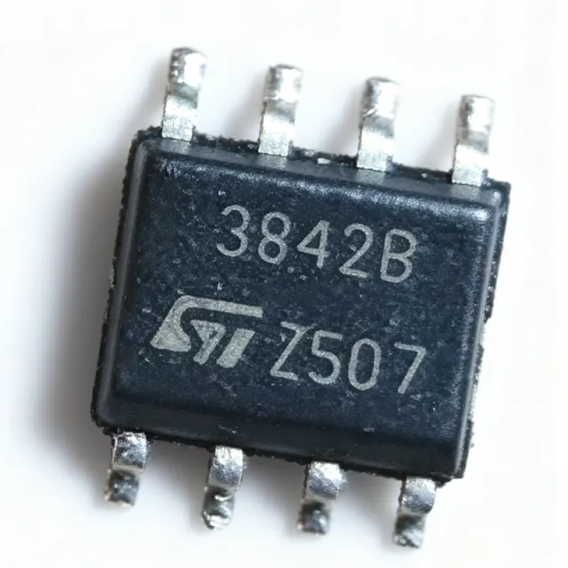
UC3842BD1 - Current Mode PWM Controller | STMicroelectronics | SMPS
The STMicroelectronics UC3842BD1 is a high-performance current-mode PWM controller designed for off-line and DC-to-DC converter applications. It operates with an input voltage range of 7.5V to 30V and provides a 1A peak output current for driving power MOSFETs. The device is available in an SOIC-8 package, making it suitable for compact power supply designs. A current-mode PWM controller is a type of switching regulator control IC that regulates output voltage by comparing the output error signal with a current-sense signal from the power switch. This architecture provides inherent feed-forward compensation, cycle-by-cycle current limiting, and simplified loop compensation compared to voltage-mode controllers. The UC3842BD1 belongs to the UC3842 family of PWM controllers, which are widely used in AC-DC adapters, battery chargers, and industrial power supplies. Key features of the UC3842BD1 include a trimmed oscillator for precise frequency control, an under-voltage lockout (UVLO) with hysteresis, a 5V reference output, and a high-gain error amplifier. The oscillator frequency is programmable up to 500 kHz, allowing designers to optimize transformer size and efficiency. The device also features a low startup current of 0.5 mA, which is critical for efficient power-up in battery-powered systems. The UC3842BD1 uses a fixed-frequency current-mode architecture with a maximum duty cycle of 96%. The error amplifier has a bandwidth of 1 MHz, enabling fast transient response. The current-sense comparator has a threshold of 1V, providing accurate cycle-by-cycle current limiting. The device is designed to operate over a junction temperature range of -40°C to +150°C, ensuring reliability in harsh environments. Typical applications include switch-mode power supplies (SMPS) for consumer electronics, industrial power converters, and battery chargers. The UC3842BD1 is also used in flyback and boost converter topologies, where its current-mode control simplifies loop compensation and improves line regulation. When designing with the UC3842BD1, ensure that the current-sense resistor is placed close to the IC to minimize parasitic inductance. The oscillator timing resistor and capacitor should be located near the RT/CT pin to reduce noise coupling. Proper grounding and decoupling of the VCC pin are essential for stable operation. This page synthesizes distributor pricing, drop-in alternatives, and practical design notes not found in the STMicroelectronics datasheet, providing engineers with a comprehensive resource for selecting and implementing the UC3842BD1.

UC3842BD1013TR - Current Mode PWM Controller | STMicroelectronics
The UC3842BD1013TR is a high-performance current-mode PWM controller from STMicroelectronics, designed for off-line and DC-to-DC converter applications. It operates as a boost or flyback regulator with isolation capability, providing a cost-effective solution for power supply designs. The device is housed in an 8-SOIC package and supports a switching frequency up to 500 kHz, with a peak output current of 1 A. Its input voltage is rated at 15 V, and it operates over a temperature range of 0°C to 70°C. A current-mode PWM controller is a type of switching regulator controller that uses the inductor current as a feedback signal to modulate the duty cycle of the output switch. This architecture provides inherent cycle-by-cycle current limiting, improved transient response, and simplified loop compensation compared to voltage-mode controllers. The UC3842BD1013TR belongs to the UC3842 family, which is widely used in AC-DC adapters, battery chargers, and isolated DC-DC converters. Key features of the UC3842BD1013TR include a trimmed oscillator for precise frequency control, current-mode operation up to 500 kHz, automatic feed-forward compensation, latching PWM for cycle-by-cycle current limiting, and an internally trimmed reference. These features enable stable and reliable operation in demanding power conversion applications. The device also includes under-voltage lockout (UVLO) and a totem-pole output stage capable of sourcing and sinking 1 A peak current to drive power MOSFET gates directly. Technically, the UC3842BD1013TR integrates a 5V reference, an error amplifier, a current-sense comparator, and a PWM latch. The oscillator frequency is set by an external resistor and capacitor, allowing designers to program the switching frequency from 50 kHz to 500 kHz. The current-sense input provides overcurrent protection by comparing the sensed voltage to a 1V threshold. The device's low startup current and low operating current contribute to high efficiency in power supplies. Typical applications include switch-mode power supplies (SMPS) for consumer electronics, industrial power converters, and isolated flyback converters for telecom and networking equipment. The UC3842BD1013TR is particularly suited for designs requiring a simple, reliable current-mode controller with minimal external components. When designing with this controller, ensure proper PCB layout to minimize noise on the current-sense and feedback paths. Use a low-ESR capacitor on the VCC pin and place the timing components close to the IC. Adequate thermal relief on the SOIC package is recommended for high-power applications.

UCC25800-Q1 - Ultra-Low EMI Transformer Driver | Texas Instruments
The Texas Instruments UCC25800-Q1 is an ultra-low EMI transformer driver designed for isolated bias supplies in automotive and industrial applications. It integrates the switching power stage, control, and protection circuits into an 8-pin HVSSOP (DGN) package with an exposed thermal pad. The device operates from a wide input voltage range of 9 V to 34 V and delivers up to 9 W from a 34-V input. It uses an LLC resonant topology, which allows the use of transformers with higher leakage inductance but much smaller parasitic primary-to-secondary capacitance, significantly reducing common-mode EMI. A transformer driver is a power management IC that generates an AC voltage from a DC input to drive an isolation transformer, providing isolated DC outputs for gate drivers, sensors, and other bias supplies. It sits within the power management hierarchy: transformer driver -> isolated bias supply -> power management IC -> semiconductor. The UCC25800-Q1 simplifies isolated bias supply design by integrating the half-bridge power stage, oscillator, and protection features, eliminating the need for external high-side drivers and complex control loops. Key features include programmable switching frequency from 0.1 MHz to 1.2 MHz, enabling optimization for transformer size and EMI. The device offers a dedicated multi-function pin for external disabling and fault code reporting, enhancing system reliability. Its ultra-low EMI performance is achieved through the LLC topology and low interwinding capacitance transformer design, making it ideal for noise-sensitive automotive environments such as electric vehicles (EVs) and hybrid electric vehicles (HEVs). The UCC25800-Q1 integrates a high-efficiency half-bridge driver with adaptive dead-time control, reducing switching losses and improving efficiency. The device includes comprehensive protection features such as overcurrent protection, thermal shutdown, and undervoltage lockout (UVLO). The 8-pin DGN package with thermal pad provides excellent thermal handling, allowing operation at high ambient temperatures up to 125°C. Typical applications include isolated gate driver bias supplies for traction inverters, on-board chargers, DC-DC converters, and battery management systems in automotive. It is also suitable for industrial isolated power supplies, motor drives, and renewable energy systems. The wide input range and programmable frequency make it versatile for various power levels and isolation requirements. When designing with the UCC25800-Q1, ensure proper transformer selection with low interwinding capacitance to maximize EMI benefits. The SYNC pin allows external synchronization, but the external frequency must be set such that half the sync frequency is between 15% and 30% of the nominal frequency to maintain output regulation. Adequate input decoupling and a low-ESR output capacitor are essential for stable operation.

UCC28019ADR - 65kHz CCM PFC Controller | Texas Instruments
The Texas Instruments UCC28019ADR is an 8-pin active Power Factor Correction (PFC) controller using boost topology in Continuous Conduction Mode (CCM). Designed for systems from 100 W to over 2 kW with wide-range universal AC line input, it operates at a fixed 65-kHz frequency with a maximum duty cycle of 98% (typ). Start-up current during undervoltage lockout is below 200 uA, and low-power standby mode is entered by pulling the VSENSE pin below 0.77 V. The DR suffix denotes the 8-pin SOIC (D) package supplied in tape and reel. A PFC controller is a specialized power management IC that shapes the input current of an AC-DC power supply to be sinusoidal and in phase with input voltage, improving power factor and reducing harmonics to meet standards such as IEC 61000-3-2. In a boost PFC, the controller regulates the DC bus voltage while forcing input current to follow input voltage. PFC controllers belong to the broader family of switch-mode power supply control ICs within power management. Key features include the 8-pin solution that reduces external component count, wide-range universal AC input, fixed 65-kHz switching, output over/under voltage protection, open-loop protection, overcurrent protection, and enhanced start-up and transient response. Average current mode control delivers stability and noise immunity, supported by an internal reference, error amplifier, and PWM comparator. UVLO thresholds are 10.5 V on and 9.5 V off, with a maximum Vin of 21 V. Typical applications include desktop computer and server power supplies, telecom rectifiers, industrial power systems, LED lighting drivers, and battery chargers that must meet power quality regulations. The controller supports both sub-150 W and above-750 W application ranges. When designing with the UCC28019ADR, keep gate drive and current-sense paths short and low inductance, place the sense resistor near the IC with a Kelvin connection, and avoid accidental triggering of the 0.77 V VSENSE standby threshold during normal operation.