제품 (38,000+)

R7S721021VCFP#AA1 - RZ/A1L 400MHz ARM Cortex-A9 MPU 3MB SRAM
R7S721021VCFP#AA1

R7S721021VCFP#AA1 - RZ/A1L 400MHz ARM Cortex-A9 MPU 3MB SRAM

The Renesas R7S721021VCFP#AA1 is an ARM Cortex-A9 microprocessor from the RZ/A1L group, operating at 400 MHz with 3 MB of on-chip SRAM, packaged in a 208-pin LFQFP (28x28 mm). Designed for compact embedded designs, it integrates rich peripherals including Ethernet, USB 2.0 host/function, CAN, LIN, SCI, SPI, I2C, UART, and an external bus interface, and is ROMless so external flash is required for code storage. A microprocessor (MPU) is an integrated circuit containing a full CPU core plus system logic, distinguished from a microcontroller (MCU) by higher processing throughput, external memory addressing, and complex peripheral integration. The RZ/A1L sits in the hierarchy: MPU -> application processor -> SoC -> RISC ARM Cortex-A family -> Renesas RZ/A1L product line. With 3 MB of embedded SRAM, the part targets graphical HMI applications where eliminating external DRAM reduces BOM cost and EOL risk. Key features of the R7S721021VCFP#AA1 include single-core 32-bit ARM Cortex-A9 at 400 MHz, 3 MB on-chip SRAM, integrated TFT LCD controller supporting up to 2x WVGA (800x480) or one WSVGA (1024x600) display, 10/100 Ethernet MAC, USB 2.0 host/function with PHY, multiple CAN/LIN/SPI/I2C interfaces, 12-bit ADC, timers, PWM, real-time clock, and watchdog timer. Architecture-wise, the Cortex-A9 core is paired with NEON SIMD and a dual-issue pipeline. The 3 MB unified SRAM can serve as frame buffer and code execution area without external DRAM, lowering system cost. The integrated TFT LCD controller with hardware-accelerated 2D graphics (raster engine) simplifies HMI design. Typical applications include industrial HMI panels, building automation control displays, home appliances with graphical UI, point-of-sale terminals, and medical device interfaces. The chip's high memory bandwidth plus display controller make it suited for graphics-rich embedded products. When designing, note that this is a ROMless device, so external NOR/NAND flash is mandatory. Power sequencing and decoupling per the Renesas hardware manual are critical for reliable boot. Use the Renesas e2studio IDE and Smart Configurator for pin and clock setup. This page synthesizes distributor stock status, drop-in alternatives, thermal/PCB guidance, and pricing benchmarks from multiple sources - engineering content complementing the manufacturer datasheet.

견적 요청 문의하기
RA8T2 - 1GHz Arm Cortex-M85 Motor Control MCU | Renesas
RA8T2

RA8T2 - 1GHz Arm Cortex-M85 Motor Control MCU | Renesas

The Renesas RA8T2 is a high-performance ASSP microcontroller featuring a 1 GHz Arm Cortex-M85 core paired with a 250 MHz Arm Cortex-M33 core, up to 1 MB of code MRAM, and 2 MB of SRAM with ECC, engineered specifically for industrial motor control applications requiring high real-time performance and high-precision control. A microcontroller (MCU) is a single-chip integrated circuit that combines a processor core, memory, and peripherals to execute dedicated control tasks. Within the hierarchy of embedded processors, the RA8T2 sits at the top of Renesas' RA family of Arm-based MCUs, above general-purpose Cortex-M4/M33 parts, and competes with high-end digital signal controllers in the industrial automation domain. Key features include over 7,000 CoreMark performance enabled by an advanced 22 nm process, advanced-function PWM and high-resolution PWM timers for precise motor drive waveforms, and high integration with a Layer 3 Ethernet Switch Module, USB 2.0 Full-Speed, CAN FD, SDHI, I3C, and Octal SPI with decryption on-the-fly. MRAM code storage provides fast, reliable non-volatile memory with high endurance compared to conventional Flash. Technically, the dual-core architecture separates high-speed field-oriented control (FOC) loops on the 1 GHz Cortex-M85 from communication stacks and supervisory tasks on the 250 MHz Cortex-M33, delivering deterministic real-time behavior. Hardware ECC on the 2 MB SRAM and functional-safety-oriented peripherals support demanding industrial equipment requirements. Typical applications include industrial servo drives, brushless DC (BLDC) and permanent magnet synchronous motor (PMSM) control, robotics, and high-end factory automation equipment where sub-microsecond control-loop latency is essential. EtherCAT-class industrial networking is supported via the Ethernet switch module. Design consideration: choose the correct speed-grade orderable part number (e.g., 1 GHz vs 600 MHz variants such as R7KA8T2LFLCAB#UC0 vs R7KA8T2AFECAB#BC1) and validate thermal design at full 1 GHz operation, as 22 nm high-frequency operation demands attention to power dissipation and PCB thermal relief. This page synthesizes distributor data, datasheet highlights, orderable-part variants, and practical design guidance not consolidated in the manufacturer datasheet alone.

견적 요청 문의하기
RC28F128P33B85B - 128Mbit NOR Flash, 52MHz, 85ns, 64-EasyBGA | Intel/Altera
RC28F128P33B85B

RC28F128P33B85B - 128Mbit NOR Flash, 52MHz, 85ns, 64-EasyBGA | Intel/Altera

The Intel/Altera RC28F128P33B85B is a 128-Mbit parallel NOR Flash memory device organized as 8M x 16, built on Intel's StrataFlash Embedded Memory technology and housed in a 64-ball EasyBGA (8x10 mm) package. It supports 2.5V/3.3V dual-voltage operation, offers 52 MHz CFI (Common Flash Interface) read throughput with 85 ns initial access time, and provides hardware-accelerated 33-bit ECC for reliable code and data storage. A NOR Flash memory is a non-volatile storage technology that provides random read access at byte or word granularity, in contrast to NAND Flash which is read in large pages. NOR Flash retains code directly executable in-place (XIP), making it the historical choice for boot ROM, firmware storage, and embedded systems where deterministic read latency matters. Within the memory hierarchy, NOR Flash sits above NAND Flash and below SRAM/DRAM, trading higher density for fast random reads and long-term data retention. Key features of the RC28F128P33B85B include 128 Mbit (16 Mbyte) density, x16 data bus, Common Flash Interface (CFI) for vendor-independent identification, 33-bit hardware ECC, and a uniform 64-Kbyte symmetric block architecture with configurable read-while-write (RWW) capability. The P33 process technology delivers lower power consumption and faster program/erase times than earlier Numonyx/Intel P30 devices. This part supports simultaneous read-while-write operations, allowing the host CPU to fetch instructions from one bank while another bank is being programmed or erased. The EasyBGA-64 (8x10 mm) package offers a compact footprint suitable for space-limited embedded designs while exposing the full multiplexed address/data bus needed for legacy parallel interfaces. Typical applications include embedded boot ROM for networking equipment, industrial control firmware storage, automotive telematics and infotainment code storage, and legacy parallel-interface designs that require deterministic read latency. The 52 MHz synchronous burst-read mode also enables higher-throughput data streaming. When designing with this device, ensure the host platform supports the legacy CFI query protocol and the 33-bit hardware ECC engine for production-grade reliability. Designers transitioning from older Numonyx/Intel P30 devices must verify pinout compatibility, as the EasyBGA ball map differs from earlier TSOP packaging. This page synthesizes distributor pricing from LCSC, DigiKey Marketplace and Octopart, drop-in package-compatible alternatives from the same P33 family, and practical design considerations not consolidated in the manufacturer datasheet.

견적 요청 문의하기
RH4Z2501BJ3GNM#HD0 - IO-Link PHY Transceiver | Renesas
RH4Z2501BJ3GNM#HD0

RH4Z2501BJ3GNM#HD0 - IO-Link PHY Transceiver | Renesas

The Renesas RH4Z2501BJ3GNM#HD0 is a single-channel IO-Link physical layer master/device transceiver with enhanced protection, housed in a 12-pin DFN (3x3 mm) package with the #HD0 tape-and-reel suffix. It functions as a line driver and level shifter IC for IO-Link communication, integrating push-pull output drivers with RDS(ON) below 2.5 ohm and tolerating supply voltage transients up to 60 V. The part supports both IO-Link master and device roles, making it suitable for sensor/actuator nodes and master-side communication. An IO-Link physical layer (PHY) transceiver is a dedicated interface IC that implements the IEC 61131-9 single-drop digital communication interface for industrial sensors and actuators. The PHY sits between the microcontroller UART/IO-Link stack and the 3-wire sensor cable (L+, L-, CQ), handling 24 V line drive levels, reverse-polarity protection, surge suppression, and the 8 mA / 16 mA / 24 mA current-sinking modes defined by the IO-Link standard. It belongs to the hierarchy: IO-Link PHY -> industrial transceiver -> interface IC -> integrated circuit -> semiconductor. Key features include configurable CQ output stages (push-pull, high-side, low-side), integrated reverse-polarity blocking on the supply pin, 60 V transient robustness on L+, an OWI (One-Wire Interface) configuration channel for parameter storage, and CMOS mixed-signal technology that supports 4.5 V to 30 V supply operation. The 12-DFN package offers a compact 3x3 mm footprint for space-constrained sensor heads. The RH4Z2501 includes internal protection features that simplify the external TVS/Schottky network typically required by IO-Link designs: over-temperature shutdown, under-voltage lockout, and reverse-polarity handling. The OWI channel allows the MCU to write configuration and identification data to on-chip non-volatile memory during end-of-line commissioning. Typical applications include IO-Link sensor signal conditioning in factory automation, IO-Link master communication modules, 24 V industrial valve and actuator drivers, and PLC digital I/O cards implementing single-drop IO-Link ports. When designing with this part, place the decoupling capacitor (10 V on L+) as close to the pin as possible and keep the CQ trace short to minimize radiated EMI. Configure the OWI address during manufacturing only - do not reconfigure OWI in the field without a controlled procedure. This page synthesizes distributor pricing, drop-in alternatives, and practical design notes for the RH4Z2501BJ3GNM#HD0 that are not found in the manufacturer datasheet alone.

견적 요청 문의하기
RK3168 - Dual-Core Cortex-A9 SoC | Rockchip | Mobile/Embedded
RK3168

RK3168 - Dual-Core Cortex-A9 SoC | Rockchip | Mobile/Embedded

The Rockchip RK3168 is a low-power, high-performance dual-core ARM Cortex-A9 SoC for smartphones, tablets, personal mobile internet devices, and digital multimedia applications. The RK3168 integrates two Cortex-A9 cores with separate NEON and FPU coprocessors, a PowerVR SGX540 GPU clocked at 400 MHz, and a hardware video decoder supporting up to 1080p H.264/MJPEG/VC-1/MPEG-4, all in a low-power BGA package. A SoC (System-on-Chip) is an integrated circuit that consolidates CPU cores, GPU, video codecs, display controllers, and peripheral interfaces on a single silicon die. Within the broader taxonomy, the RK3168 belongs to the application processor family, sitting between a microcontroller (no display/multimedia capability) and a full multimedia SoC. The Cortex-A9 microarchitecture places the RK3168 in the mid-2010s generation of ARMv7 application processors, which succeeded the Cortex-A8 and was later overtaken by Cortex-A53/A55 designs. Key features include dual-core 1.2 GHz Cortex-A9 with out-of-order execution, PowerVR SGX540 graphics, integrated HDMI/LVDS display controllers, USB 2.0 OTG, MIPI CSI camera interface, multiple SDIO/EMAC/SD card controllers, and a hardware crypto block. The SoC is fabbed on a low-power process with typical smartphone power dissipation below 1 W, enabling fanless designs in tablets and set-top boxes. Architecturally, the RK3168 uses a dual-core Cortex-A9 with NEON SIMD for media acceleration and a separate VPU (Video Processing Unit) that offloads 1080p decode from the CPU. This hardware partitioning delivers the multimedia performance of higher-priced application processors while maintaining the power profile of mobile devices. The SGX540 GPU provides OpenGL ES 2.0 and OpenVG 1.1 support suitable for 3D UI and casual gaming. Typical applications include Android smartphones and tablets in the 7-10 inch class, Miracast/dongle wireless display adapters, low-cost media players and set-top boxes, in-vehicle infotainment (IVI) systems, and industrial HMI panels. The Miracast reference design (RK3168 + Wi-Fi companion chip) became a $10 retail adapter form factor in 2013. When designing with this part, ensure the PCB stack-up meets the BGA escape routing requirements and provide adequate thermal relief on the package substrate. Designers should pair the RK3168 with LPDDR2 or DDR3 memory validated by Rockchip's hardware reference manual to avoid boot issues. This page synthesizes distributor pricing, datasheet details, and Rockchip family alternatives not available on a single manufacturer datasheet, helping procurement engineers and engineering teams source the part with confidence.

견적 요청 문의하기
RK3288 - Quad-Core Cortex-A17 SoC | Rockchip | BGA-636
RK3288

RK3288 - Quad-Core Cortex-A17 SoC | Rockchip | BGA-636

The Rockchip RK3288 is a low-power, high-performance 32-bit quad-core application processor built around four ARM Cortex-A17 cores with a separately clocked NEON SIMD coprocessor and an ARM Mali-T764 GPU, packaged in a 636-ball BGA. It is designed for mobile phones, personal mobile internet devices (PMID), and other digital multimedia applications, integrating CPU, GPU, multimedia, memory controller, and peripheral I/O into a single SoC. A quad-core application processor (AP) is a system-on-chip that integrates multiple CPU cores, a graphics processor, memory interfaces, display controllers, and standard peripherals (USB, SDIO, I2C, SPI, UART, Ethernet, HDMI, LVDS, MIPI) on a single die. In a system architecture, the AP sits between power management ICs (PMICs), DRAM (LPDDR2/LPDDR3/DDR3), and the display/camera subsystems. The RK3288 belongs to a broader family of Rockchip ARM APs and is part of the Cortex-A17 generation that targeted Android tablets, set-top boxes, Chromebooks, and digital signage during the mid-2010s. Key features include quad-core ARM Cortex-A17 up to 1.8 GHz, Mali-T764 GPU with OpenGL ES 3.1 support, hardware-accelerated 4K H.264/H.265 video decode, HDMI 2.0 output up to 4K@60Hz, dual-channel 32-bit LPDDR3/DDR3/LPDDR2 interface, MIPI DSI and LVDS display outputs, USB 2.0, SD/MMC, eMMC 5.0 support, and integrated audio codec with SPDIF/I2S. The chip supports Android 5.x/6.x and Linux kernels, making it a versatile multimedia AP for consumer and embedded OEMs. The RK3288 uses a 28 nm HKMG CMOS process, which balances performance with reasonable power consumption. Its quad-core Cortex-A17 out-of-order design delivers significantly higher single-threaded performance than the Cortex-A9 predecessor (RK3188) and enables efficient multitasking. The Mali-T764 GPU supports modern graphics APIs, while the 4K hardware codec block offloads video decode from the CPU cores. Typical applications include Android tablets, Chromebooks, digital signage, smart home control panels, set-top boxes, industrial HMI terminals, and embedded kiosks. Designers choose the RK3288 when they need a mature quad-core Cortex-A17 SoC with strong multimedia capabilities and broad Linux/Android BSP support. When designing with the RK3288, pay attention to PCB layout for the BGA-636 footprint - it requires microvia / HDI PCB technology for reliable BGA escape routing. Thermal management is critical because the SoC can dissipate 2 to 5 W under full CPU+GPU+4K decode load. Use a multi-layer PCB with a continuous ground plane under the BGA and provide adequate copper thermal relief around the package. Validate the PMIC compatibility (e.g., RK808 or ACT8846 family) and DRAM timing margins before committing to volume production. This page synthesizes distributor pricing, drop-in same-package Rockchip SoC variants, application pairings, and practical PCB/system design notes not typically consolidated in the manufacturer datasheet.

견적 요청 문의하기
RK3368 - Octa-Core 64-bit ARM Cortex-A53 SoC | Rockchip
RK3368

RK3368 - Octa-Core 64-bit ARM Cortex-A53 SoC | Rockchip

The Rockchip RK3368 is a low-power, high-performance 64-bit application processor integrating an octa-core ARM Cortex-A53 CPU cluster with separately clocked NEON coprocessors and an ARM Mali-T720MP2 GPU, targeted at smart TV boxes, OTT streaming devices, set-top boxes, and personal mobile internet devices. The part is manufactured in a 28 nm HPC process, supports up to 1.5 GHz core frequency, integrates 4K H.265/H.264 hardware decoding, HDMI 2.0 output up to 4K@60 Hz, and dual-channel DDR3/DDR3L/LPDDR2/LPDDR3 memory controllers. The RK3368 ships in a 19 mm x 19 mm BGA-453 package (0.8 mm pitch) and is specified for commercial-grade operation at 0 C to +80 C ambient. What is an application processor SoC? An application processor SoC (System-on-Chip) integrates the CPU, GPU, memory controller, video decoder/encoder, display pipeline, and connectivity peripherals onto a single silicon die. In the broader taxonomy: SoC -> application processor -> microprocessor unit (MPU) -> semiconductor. Rockchip positions the RK3368 in its 64-bit octa-core family below the RK3399 (big.LITTLE A72+A53) and above the entry-level RK3328 (quad-core A53). Key features include 64-bit ARMv8 instruction set with full AArch64 execution, hardware H.265 Main Profile decoding up to 4K@60 Hz with H.265 Main10 support, OpenGL ES 3.1 / OpenCL 1.2 capable Mali-T720MP2 GPU running at up to 600 MHz, USB 2.0 host and OTG ports, Gigabit Ethernet MAC, and a flexible VOP (Video Output Processor) supporting HDMI 2.0, eDP, and MIPI-DSI. The integrated Cortex-A53 cores provide 2-3x the performance-per-watt of the previous-generation Cortex-A7 used in the RK3288. The RK3368 architecture uses a single homogeneous octa-core cluster with coherent L2 cache, simplifying software scheduling compared to big.LITTLE designs. The 28 nm process keeps idle power low, while the integrated LPDDR3 controller with 32-bit width and 800 MHz clock provides up to 6.4 GB/s memory bandwidth suitable for 4K video decode. Typical applications include 4K Android TV boxes, OTT streaming sticks, smart signage players, industrial HMI panels, and education tablets. The Cortex-A53's power efficiency also makes the part suitable for fanless enclosures. Design consideration: the RK3368 requires careful 4-layer or 6-layer PCB stack-up with matched-length DDR3 traces and a robust PMIC (RK806 or compatible). LPDDR3 routing demands 100 ohm differential impedance; deviations will cause read/write errors at high temperatures. This page synthesizes distributor pricing, drop-in Rockchip alternatives (same BGA-453 family where applicable), and design notes not consolidated in the public RK3368 datasheet.

견적 요청 문의하기
RMLV0816BGSD-4S2 - 8Mb Low-Power SRAM 512Kx16 45ns TSOP | Renesas
RMLV0816BGSD-4S2

RMLV0816BGSD-4S2 - 8Mb Low-Power SRAM 512Kx16 45ns TSOP | Renesas

The Renesas RMLV0816BGSD-4S2 is an 8-Mbit Advanced Low-Power Static RAM organized as 524,288-word x 16-bit (512K x 16), fabricated on Renesas' high-performance Advanced LPSRAM process technology. The device is offered in a 52-pin TSOP-II package and delivers 45 ns parallel access time, making it suitable for low-power embedded systems that require fast random read/write cycles. An LPSRAM (Low-Power SRAM) is a class of asynchronous static random-access memory that retains data without refresh and is optimized for ultra-low standby current consumption. LPSRAMs occupy a distinct position in the memory hierarchy: faster than NOR flash, lower pin-count than DRAM (no refresh controller required), and dramatically lower quiescent current than legacy SRAM - typically in the microamp range. They are widely used as working RAM, data buffers, and backup-memory companions to MCUs in industrial and consumer designs. Key features of the RMLV0816BGSD-4S2 include a single 2.7 V to 3.6 V supply, 45 ns address access time, fully static asynchronous operation (no clock required), TTL-compatible I/O, three-state outputs, and an operating temperature range of -40 C to +85 C for the industrial grade variant. The device supports byte-wise control via /LB and /UB pins for 8-bit/16-bit flexible access, plus standard /CS, /OE, and /WE control signals. Advanced LPSRAM technology achieves low standby current while maintaining fast access, suitable for battery-backed applications. Architecturally, the RMLV0816BGSD-4S2 employs a 6-transistor (6T) CMOS memory cell array with on-chip sense amplifiers and self-timed write circuitry. The advanced LPSRAM process allows smaller cell size while preserving the low-leakage characteristics that define the family. Internal address latches and a common I/O bus enable efficient 8-bit (byte) and 16-bit (word) access without external logic. Typical applications include industrial controls, factory automation PLCs, networking line cards, portable instrumentation, medical devices, POS terminals, and any battery-backed data-logging system requiring reliable byte-wide or word-wide buffering. Designers often pair this LPSRAM with low-power MCUs such as Renesas RX or RA families for energy-harvesting or sleep-mode designs. A key design consideration is the decoupling strategy: place a 0.1 uF ceramic bypass capacitor within 5 mm of the VCC pin and a 10 uF bulk capacitor on the supply rail. Avoid driving the I/O bus faster than the rated access time to prevent bus contention during read/write transitions. This page synthesizes distributor pricing, drop-in alternatives, and practical design notes not found in the manufacturer datasheet.

견적 요청 문의하기

RMLV0816BGSD-4S2#AC0 - 8Mb Advanced LPSRAM | Renesas | TSOP-II 52
RMLV0816BGSD-4S2#AC0

RMLV0816BGSD-4S2#AC0 - 8Mb Advanced LPSRAM | Renesas | TSOP-II 52

The Renesas RMLV0816BGSD-4S2#AC0 is an 8-Mbit advanced low-power static RAM organized as 524,288-word × 16-bit (or 1M × 8), fabricated on Renesas's high-performance Advanced LPSRAM process. The device operates from a single 2.4V to 3.6V supply, provides 45 ns access time, and ships in a 52-pin TSOP-II surface-mount package. It is part of the RMLV0816BGSD family aimed at embedded systems that need byte-wide or word-wide battery-backed memory. A low-power SRAM (LPSRAM) is a type of volatile static random-access memory that retains data without refresh cycles and consumes very low standby current, making it the preferred choice for battery-powered or always-on subsystems. Within the broader memory hierarchy, LPSRAM sits between small on-chip MCU SRAM and larger DRAM, filling the role of fast, byte-addressable working memory. Compared to DRAM, LPSRAM eliminates the need for periodic refresh, simplifies board design, and improves immunity to bit errors caused by particle hits, at the cost of lower density per die. Key features of the RMLV0816BGSD-4S2 include a wide 2.4V–3.6V single-supply range, 45 ns access time, byte-control via UB#/LB# pins for x16 operation, support for x8 / x16 bus width selection, and very low standby current. The 52-TSOP II footprint is the industry-standard pinout for 8-Mbit word-wide SRAM, allowing it to replace legacy parallel SRAMs from Cypress, ISSI, and Alliance on existing PCB layouts. The Advanced LPSRAM cell technology keeps active current low while delivering fast read/write cycles for data logging or boot-loader scratchpad use. Internally, the die uses a six-transistor (6T) SRAM cell with CMOS I/O, including a chip-enable (CE#), write-enable (WE#), output-enable (OE#), and upper/lower byte select (UB#/LB#) for flexible bus sizing. The wide voltage range is achieved through on-chip charge-pump-free regulation, so no external VCCQ or VPP rail is required. The 45 ns access time is sufficient for direct connection to most microcontrollers and low-end microprocessors without wait-state insertion at ≤33 MHz, which covers typical MCU-class applications. Typical applications for the RMLV0816BGSD-4S2 include industrial control data buffers, metering and instrumentation scratch memory, networking router packet buffers, automotive infotainment working memory, and battery-backed data retention when paired with an external supercapacitor or coin cell. The wide 2.4V–3.6V range also suits USB, Bluetooth, and Zigbee module working memory. When designing with this part, ensure that decoupling (0.1 µF + 10 µF bulk) is placed within 5 mm of VCC, and respect the data retention voltage (typically 2.0V) if you intend to operate from a battery backup rail. UB# and LB# must be tied low for full 16-bit access; leaving them floating introduces bus contention and increases standby current. This page synthesizes Renesas datasheet parameters, distributor pricing as of 2026-10-10, same-package Renesas drop-in alternatives, and cross-package notes not found in the manufacturer datasheet.

견적 요청 문의하기
RMWV3216AGBG-5S2#AC0 - 32Mb Advanced LPSRAM, 2Mx16, 55ns | Renesas
RMWV3216AGBG-5S2#AC0

RMWV3216AGBG-5S2#AC0 - 32Mb Advanced LPSRAM, 2Mx16, 55ns | Renesas

The Renesas Electronics RMWV3216AGBG-5S2#AC0 is a 32-Mbit Advanced Low-Power SRAM (LPSRAM) organized as 2,097,152 words × 16 bits, fabricated in Renesas's high-performance Advanced LPSRAM CMOS technology. It is offered in a 48-ball TFBGA package measuring 7.5 mm × 8.5 mm, operates from a single 2.7 V to 3.6 V supply, and delivers a 55 ns fast access time in parallel mode. The I-temperature grade (-40 °C to +85 °C) makes it suitable for industrial environments. An LPSRAM (Low-Power SRAM) is a class of asynchronous static random-access memory that retains data without refresh and offers dramatically lower active and standby current than conventional SRAM. LPSRAM sits in the broader memory hierarchy between volatile DRAM (which needs refresh and is dense) and true non-volatile memory (Flash/EEPROM, which is slow to write). Within Renesas's portfolio, Advanced LPSRAM targets battery-backed and energy-harvesting applications where every microwatt of quiescent current matters, while still delivering the byte-level random access that Flash cannot. Key features include very low standby current for battery-backup retention, a wide 2.7 V to 3.6 V single-rail supply range that simplifies power-tree design, common parallel SRAM interface pinout (CS, OE, WE, UB/LB byte enables) for drop-in replacement of legacy async SRAMs, and 3-STATE outputs for bus-sharing. The 48-ball TFBGA footprint is also substantially smaller than TSOP or SOJ packaging used by older 32-Mbit parallel SRAMs. Technically, the device uses a six-transistor (6T) CMOS memory cell array with on-chip address decoding and sense amplifiers, plus internal voltage generation for the memory core. The die is organized as 2M × 16 with separate upper-byte and lower-byte write enables (UB, LB), which simplifies 8-bit and 16-bit bus designs in the same socket. Power-saving features include automatic power-down when CS is deselected, plus data-retention modes down to 2.0 V for coin-cell backup. Typical applications include industrial metering and data loggers, factory automation controllers, point-of-sale terminals, automotive infotainment buffers, medical handheld instruments, networking line cards requiring fast read/write buffers, and battery-backed equipment such as e-meter or PLC retentive memory. The low standby current makes it attractive as a shadow RAM for systems that must preserve state through power loss. When designing with this part, follow the datasheet's decoupling guideline of a 0.1 µF ceramic capacitor placed within 5 mm of each VCC ball, plus a bulk 10 µF tantalum or ceramic on the supply rail. Place the device close to the host controller to keep the address/data bus traces short, since the 55 ns access time assumes modest capacitive loading. This page synthesizes distributor pricing and stock, drop-in alternative comparisons across Renesas's own RMWV3216A speed-grade family and competing 48-ball TFBGA LPSRAMs, and practical design notes not consolidated in the manufacturer datasheet.

견적 요청 문의하기
RS512M16Z2DD-62DT - 8Gbit DDR4 SDRAM 512Mx16 | Rayson
RS512M16Z2DD-62DT

RS512M16Z2DD-62DT - 8Gbit DDR4 SDRAM 512Mx16 | Rayson

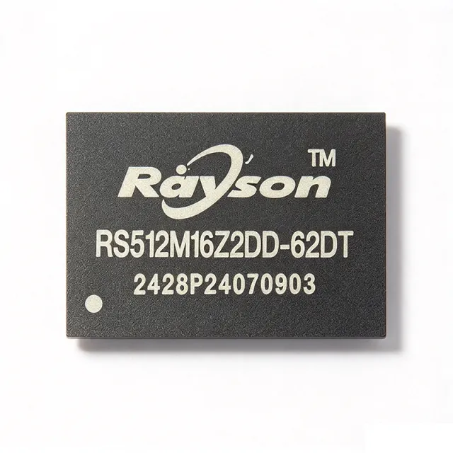
The Rayson RS512M16Z2DD-62DT is a high-performance DDR4 SDRAM (Double Data Rate Fourth Generation Synchronous Dynamic Random-Access Memory) device organized as 512M words by 16 bits, providing a total density of 8Gbit. It operates at a data rate of 3200 Mb/s/pin (DDR4-3200) with a CAS latency of 22, and is housed in a compact FBGA-96 package measuring 7.5x13 mm. This memory component is designed for mission-critical applications in industrial automation, telecommunications, edge computing, and embedded systems that require robust memory performance across extended temperature ranges. DDR4 SDRAM is the fourth generation of double data rate synchronous dynamic random-access memory, succeeding DDR3. It achieves higher speed and lower power consumption through a prefetch of 8n, a lower operating voltage of 1.2V, and improved signal integrity features such as on-die termination (ODT) and write leveling. DDR4 is a key component in modern computing systems, serving as the main memory for processors, and is also used in networking equipment, servers, and high-performance embedded designs. Key features of the RS512M16Z2DD-62DT include an operating temperature range of 0°C to +95°C, a supply voltage of 1.14V to 1.26V for VDD and 2.375V to 2.75V for VDDQ, and a clock frequency of 1.6GHz. It supports auto self-refresh, auto precharge, asynchronous reset, data mask, CRC, dynamic on-chip termination, ZQ calibration, and write leveling functions. These features ensure reliable operation and data integrity in demanding environments. The device utilizes advanced DDR4 architecture with a 16-bit I/O interface, enabling high-bandwidth data transfer. The FBGA-96 package provides excellent thermal and electrical performance, with a ball pitch that supports high-density PCB routing. The 512Mx16 organization is ideal for applications requiring large memory capacity with a moderate bus width, balancing density and pin count. Typical applications include industrial automation controllers, telecommunications infrastructure, edge computing gateways, and embedded systems that require high-speed, reliable memory. The wide temperature range and robust feature set make it suitable for harsh environments where standard commercial memory might fail. When designing with this DDR4 device, ensure proper termination and signal integrity practices are followed, including controlled impedance traces and appropriate on-die termination settings. The ZQ calibration pin must be connected to a 240-ohm resistor to ground for proper calibration.

USD $30.80 재고 있음
RTAX1000S-1LG624V - 1M-Gate Rad-Tolerant FPGA | Microchip
RTAX1000S-1LG624V

RTAX1000S-1LG624V - 1M-Gate Rad-Tolerant FPGA | Microchip

The Microchip Technology RTAX1000S-1LG624V is a radiation-tolerant antifuse FPGA delivering 1,000,000 equivalent system gates with 12096 CLBs, 18144 logic cells, and up to 418 user I/Os, housed in a 624-ball ceramic column grid array (LG624) package. A radiation-tolerant FPGA is a field-programmable gate array engineered to survive the ionizing radiation and single-event effects encountered in orbital and deep-space environments. Unlike reprogrammable SRAM FPGAs, the RTAX-S family uses nonvolatile antifuse technology, in which permanent interconnects are formed at one-time programming. This eliminates configuration-storage vulnerabilities, gives true live-at-power-up operation, and makes the device a single-chip solution in the power management hierarchy of spacecraft avionics systems. Key features include one-time-programmable antifuse interconnect with no external configuration PROM, up to 540 kbits of embedded SRAM with optional EDAC protection, segmentable clock resources, chip-wide highway routing, and carry logic inherited from the commercial Axcelerator architecture. Total ionizing dose tolerance is 300 krad (functional) and 200 krad (parametric), with SEU rates below 1E-10 errors per bit-day. The CMOS architecture achieves a maximum combinatorial delay of 0.93 ns on the -1 speed grade. Embedded FIFO control logic and dual-port SRAM blocks support on-board data processing, telemetry formatting, and payload signal chains without external memory in many designs. Typical applications include satellite payload processing, spacecraft telemetry and command interfaces, radiation-hardened bus controllers, and Earth-observation instrument data acquisition where live-at-power-up behavior is mandated. Design consideration: because the device is one-time programmable, complete functional simulation and a prototyping pass on the pin-mapped commercial Axcelerator device via Microchip Extender boards or Aldec CG624 adaptor boards are strongly recommended before committing flight parts. This page synthesizes distributor availability data, same-footprint drop-in alternatives, and space-flight design guidance not consolidated on the manufacturer product page.

견적 요청 문의하기
RTAX1000SL-1CQ352V - 1M-Gate Rad-Tolerant Antifuse FPGA | Microchip
RTAX1000SL-1CQ352V

RTAX1000SL-1CQ352V - 1M-Gate Rad-Tolerant Antifuse FPGA | Microchip

The Microchip Technology (Actel/Microsemi) RTAX1000SL-1CQ352V is a radiation-tolerant, antifuse-based FPGA delivering 1,000,000 equivalent system gates with 12,096 CLBs and 18,144 logic cells, housed in a 352-pin ceramic quad flat pack (CQ352) package with military/space screening per the -V ordering suffix. A radiation-tolerant FPGA is a field-programmable gate array qualified to survive the total ionizing dose (TID) and single-event effect (SEE) environments encountered in space flight. Within the power-management hierarchy of spacecraft avionics, the RTAX-S/SL family sits at the top of Microchip's rad-hard logic portfolio: FPGA -> radiation-tolerant programmable logic -> space-grade IC. Unlike flash- or SRAM-based FPGAs, the RTAX-S/SL family uses antifuse programmable interconnect that is one-time programmed, providing live-at-power-up operation with no external configuration storage required. Key features include 1,000,000 system gates of capacity, embedded SRAM blocks with built-in FIFO control logic, segmentable clock resources, chip-wide highway routing, and dedicated carry logic for arithmetic chains. Because the configuration is locked into the antifuse fabric, the device is immune to configuration upsets that plague SRAM FPGAs, dramatically reducing SEU-driven system-level mitigation overhead. The RTAX1000SL is based on the commercial Axcelerator architecture, so designers can prototype on cost-effective Axcelerator devices and migrate using Microchip's footprint-compatible adaptor board methodology and EDIF netlist/pinout conversion flow described in the RTAX-S/SL datasheet. Typical applications include spacecraft avionics buses, satellite payload data processing, telemetry/command interfaces, and instrument control in low-Earth-orbit and deep-space missions where low power and single-chip form factor matter. A key design consideration: antifuse devices are one-time programmable, so functional verification (simulation and hardware prototyping on Axcelerator equivalents) must be completed before programming flight units. This page synthesizes distributor sourcing data, drop-in same-package alternatives, and practical design notes not found in the manufacturer datasheet.

견적 요청 문의하기
RTAX1000SL-1LG624V - 1M-Gate Rad-Tolerant FPGA | Microchip
RTAX1000SL-1LG624V

RTAX1000SL-1LG624V - 1M-Gate Rad-Tolerant FPGA | Microchip

The Microchip Technology RTAX1000SL-1LG624V is a radiation-tolerant Field Programmable Gate Array (FPGA) from the RTAX-SL family delivering 1,000,000 equivalent system gates, 18,144 logic cells, and 12,096 CLBs in a 624-pin LG (LGA) package. Built on 0.15 um CMOS process technology at a 1.5V core voltage, it offers a maximum CLB combinatorial delay of 0.93 ns. A radiation-tolerant FPGA is a programmable logic device qualified for space-flight environments, where cosmic rays and trapped-particle radiation would corrupt or destroy commercial FPGAs. The RTAX-SL family sits within the broader hierarchy: FPGA -> radiation-tolerant FPGA -> space-grade programmable logic, and is based on the commercial Actel Axcelerator architecture with anti-fuse one-time-programmable interconnect that is inherently immune to configuration upsets. Key differentiating features include true single-chip operation (no external configuration PROM required), live-at-power-up functionality, low static power consumption, embedded SRAM blocks with built-in FIFO control logic, segmentable clock resources, and chip-wide highway routing. The one-time-programmable anti-fuse fabric eliminates the need for SEU-sensitive configuration memory, a major system-level advantage in orbit. Architecturally, the device combines combinatorial and sequential logic modules (CLBs) with dedicated embedded SRAM and high-speed interconnect derived from Axcelerator, supporting system performance up to hundreds of MHz while remaining latch-up immune and tolerant to total ionizing dose. Typical applications include satellite payload processing, spacecraft telemetry and command interfaces, orbital instrument control, and spaceflight avionics bus bridges where single-chip, low-power, radiation-tolerant logic is mandatory. Designers should note that anti-fuse programming is irreversible: finalize the design using the footprint-compatible prototyping flow before committing flight units. This page synthesizes verified distributor data, drop-in family alternatives, and design guidance not consolidated in the manufacturer datasheet.

견적 요청 문의하기
RTAX1000SL-LG624V - Rad-Tolerant FPGA, 1M Gates | Microchip
RTAX1000SL-LG624V

RTAX1000SL-LG624V - Rad-Tolerant FPGA, 1M Gates | Microchip

The Microchip Technology (Microsemi/Actel) RTAX1000SL-LG624V is a radiation-tolerant, antifuse-based field-programmable gate array (FPGA) delivering 1,000,000 equivalent system gates with 12,096 configurable logic blocks (CLBs) in a 624-terminal ceramic column grid array (CGA) package qualified for space-flight environments. A radiation-tolerant FPGA is a semiconductor device designed to operate reliably in the presence of cosmic radiation and solar particle events found in space orbits. Within the semiconductor hierarchy, it belongs to the programmable logic family: FPGA -> programmable logic IC -> digital integrated circuit. Unlike SRAM FPGAs, the RTAX-S/SL family uses antifuse technology, meaning configuration is permanent and non-volatile - the device is live-at-power-up with no external configuration memory required. Key features include single-chip form factor, low-power CMOS operation, built-in FIFO control logic within embedded SRAM blocks, segmentable clock structures, chip-wide highway routing, and dedicated carry logic for arithmetic functions. The related RTAX1000SL-1LG624V speed-grade variant specifies a maximum CLB combinatorial delay of 0.93 ns, indicating the family's high-speed capability. The RTAX-S architecture is based on the commercial Axcelerator device family, providing designers with proven system-level features while adding radiation tolerance through process and design hardening. Designers program the device once, and the antifuse connections retain the design through power cycles and radiation exposure - a critical property for launcher electronics, satellites, and planetary probes. Typical applications include satellite payload processing, spacecraft command and data handling, telemetry and telecommand interfaces, bus controllers, and radiation-exposed instrumentation for low-Earth-orbit and deep-space missions. When designing with this device, plan the power budget around the CMOS static current plus dynamic switching, and use Microchip's Libero SoC design suite with the provided footprint-compatible prototyping flow. This page synthesizes distributor stock listings, family datasheet parameters, drop-in alternative analysis, and practical design notes not consolidated in the manufacturer datasheet alone.

견적 요청 문의하기
RTAX2000D-1CQ352E - 2M-Gate Rad-Tolerant FPGA CQFP352 | Microchip
RTAX2000D-1CQ352E

RTAX2000D-1CQ352E - 2M-Gate Rad-Tolerant FPGA CQFP352 | Microchip

The Microchip Technology RTAX2000D-1CQ352E is a 2,000,000-equivalent-gate radiation-tolerant antifuse FPGA organized as 19,712 Configurable Logic Blocks (CLBs), housed in a 352-terminal ceramic quad flat pack (CQFP352) and specified for operation from -55C to +125C. It belongs to the RTAX-S/SL and RTAX-DSP family of high-reliability, nonvolatile antifuse FPGAs designed for space-based applications. A radiation-tolerant FPGA is a field-programmable gate array engineered to survive the ionizing radiation environment of orbital and deep-space missions, where commercial devices would suffer total ionizing dose (TID) degradation and single-event effects. Within the power-management and processing hierarchy of a spacecraft avionics system, an FPGA such as the RTAX2000D sits between the onboard computer and sensor/interface electronics, implementing glue logic, bus interfaces, and high-throughput datapath functions. Key features include highly reliable nonvolatile antifuse technology, which retains its programmed configuration permanently and eliminates configuration-memory upset, and a DSP-rich architecture with up to 120 DSP mathblocks supporting 125 MHz 18-bit x 18-bit multiply-accumulate operations. Embedded memory extends to 540 kbits with optional EDAC protection, mitigating single-event upsets in on-chip SRAM. The RTAX2000D is a digital CMOS device based on the commercial Axcelerator architecture, with the radiation-tolerant RT variant distinguished by screening of ICCA current limits at 125C final electrical test. TID performance is 300 krad (functional) and 200 krad (per the RTAX-DSP family characterization), enabling multi-year missions in medium Earth orbit and beyond. Typical applications include spacecraft command and data handling, payload processing and sensor-data formatting, and telecommunications payload beam-forming, where the DSP mathblocks accelerate filtering and FFT workloads. Design consideration: antifuse FPGAs are one-time-programmable; prototypes should be validated on commercial Axcelerator Extender boards before flight-unit programming. This page synthesizes distributor sourcing data, drop-in alternatives, and practical design notes not found in the manufacturer datasheet.

견적 요청 문의하기
RTAX2000D-CQ352B - 2M-Gate Rad-Tolerant FPGA, CQFP-352 | Microchip
RTAX2000D-CQ352B

RTAX2000D-CQ352B - 2M-Gate Rad-Tolerant FPGA, CQFP-352 | Microchip

The Microchip (Actel/Microsemi) RTAX2000D-CQ352B is a radiation-tolerant, antifuse-based FPGA with 2,000,000 equivalent system gates, 29,568 logic cells organized as 19,712 CLBs, and a 1.5V core supply, housed in a 352-pin ceramic quad flat pack (CQFP-352) with burn-in screening (B suffix). A radiation-tolerant FPGA is a programmable logic device qualified for space-flight environments where total ionizing dose (TID) and single-event effects threaten conventional SRAM FPGAs. Within the power-management hierarchy of space avionics, the RTAX family sits in the on-board data processing tier, providing single-chip glueless logic that is live at power-up because its antifuse configuration is permanently programmed. Key features include antifuse one-time-programmable interconnect immune to configuration upsets, embedded SRAM blocks with built-in FIFO control logic, segmentable clock resources, chip-wide highway routing, and carry logic for arithmetic chains. The D-suffix die is screened with tighter ICCA current limits at 125C final electrical test compared to the standard RTAX2000S, supporting high-reliability programs. Architecturally, the RTAX2000D derives from the commercial Axcelerator family, using a 0.15-micron CMOS process with metal-to-metal antifuse elements. This yields low static power, no configuration PROM requirement, and no SEE-sensitive configuration memory, a decisive advantage over SRAM-based FPGAs in orbit. Typical applications include satellite payload data processing, spacecraft bus command and telemetry controllers, sensor interface and formatting logic, and radiation-hardened reconfigurable computing modules. Design-wise, plan the migration path: prototype against Axcelerator commercial parts using the footprint-compatible adaptor board and EDIF netlist/pinout conversion methodology described in the manufacturer datasheet before committing to the one-time-programmable RTAX device. This page synthesizes distributor availability, drop-in family alternatives, and design guidance not consolidated in the manufacturer datasheet.

견적 요청 문의하기
RTAX2000D-CQ352V - 2M-Gate Rad-Tolerant FPGA CQFP352 | Microchip
RTAX2000D-CQ352V

RTAX2000D-CQ352V - 2M-Gate Rad-Tolerant FPGA CQFP352 | Microchip

The Microchip Technology RTAX2000D-CQ352V is a radiation-tolerant, antifuse-based FPGA offering 2,000,000 equivalent system gates, 29,568 logic cells, and 19,712 configurable logic blocks (CLBs), housed in a 352-pin ceramic quad flat pack (CQFP352) with 0.500 mm terminal pitch. A radiation-tolerant FPGA is a field-programmable gate array engineered to survive the ionizing radiation environment of space, where total ionizing dose (TID) and single-event effects would degrade or destroy commercial silicon. Within the semiconductor hierarchy, the RTAX2000D-CQ352V belongs to the RTAX-S/SL and RTAX-DSP family of rad-tolerant FPGAs, derived from the commercial Axcelerator architecture, and sits in the broader category of programmable logic devices (PLDs) alongside CPLDs and structured ASICs. Key features include one-time-programmable antifuse configuration, which is inherently immune to configuration memory upsets caused by single-event effects; a nominal 1.5V core supply (1.425V to 1.575V range); and embedded SRAM blocks with built-in FIFO control logic for on-chip data buffering. The 'D' designation denotes the die lot, and the 'V' suffix indicates the qualification screening flow applied at final test. Architecturally, the device uses segmentable clock resources and chip-wide highway routing to distribute high-speed clocks and wide buses with low skew, supporting system-level integration typical of space-flight payload and platform electronics. Typical applications include satellite payload data processing, spacecraft bus control electronics, telemetry and telecommand interfaces, and radiation-hardened signal processing chains where reprogrammable SRAM FPGAs are unacceptable due to upset sensitivity. A key design consideration is that antifuse FPGAs cannot be reprogrammed after programming; design flows therefore rely on the footprint-compatible prototyping methodology using adaptor boards (such as the Aldec ACT-H3Ki-CQ352) before committing flight hardware. This page synthesizes distributor listings, family cross-references, and drop-in alternative data not consolidated in the manufacturer datasheet.

견적 요청 문의하기
RTAX2000DL-CQ352B - 2M-Gate Rad-Tolerant FPGA | Microchip
RTAX2000DL-CQ352B

RTAX2000DL-CQ352B - 2M-Gate Rad-Tolerant FPGA | Microchip

The Microchip Technology RTAX2000DL-CQ352B is a radiation-tolerant antifuse FPGA from the RTAX-DSP family delivering 2,000,000 equivalent system gates organized as 19,712 CLBs, with up to 120 DSP mathblocks performing 18-bit x 18-bit multiply-accumulate at 125 MHz, housed in a 352-terminal ceramic quad flat pack (CQFP) with a 0.500 mm terminal pitch. A radiation-tolerant FPGA is a programmable logic device qualified for spaceflight environments, where total ionizing dose (TID), single-event effects, and reliability dominate the design hierarchy. The RTAX family sits within the broader taxonomy of FPGAs -> radiation-tolerant programmable logic -> space-grade semiconductors, and derives its architecture from the commercial Microsemi (Actel) Axcelerator family. Key features include nonvolatile antifuse programming technology, which is live-at-power-up and requires no configuration PROM, single-chip form factor, embedded SRAM blocks totaling up to 540 kbits with optional EDAC protection, segmentable clocks, and chip-wide highway routing. The DL variant integrates dedicated DSP mathblocks, offloading multiply-accumulate operations from general-purpose logic and dramatically improving FFT and FIR filter throughput per watt. Technically, the device is fabricated in CMOS and operates from a nominal 1.5V core supply (1.425V to 1.575V range per Microchip data). Radiation performance includes functional operation to 300 krad (Si) total ionizing dose and 200 krad (Si) for related parameters, per the RTAX-S/SL and RTAX-DSP datasheet. The hermetic ceramic metal-sealed CQFP package supports the outgassing and reliability requirements of spaceflight assembly. Typical applications include satellite payload processing, onboard image and signal processing, spacecraft bus controllers, and telemetry/telecommand systems - anywhere high DSP throughput must coexist with radiation tolerance and single-chip simplicity. A critical design consideration is that antifuse FPGAs are one-time programmable: any logic change requires a physical board replacement, so extensive pre-flight simulation and in-orbit flexibility trade-offs must be evaluated against SRAM-based alternatives. This page synthesizes verified distributor data, drop-in alternatives, and practical design notes not found in the manufacturer datasheet.

견적 요청 문의하기
RTAX2000DL-CQ352E - 2M-Gate Rad-Tolerant FPGA CQFP-352 | Microchip
RTAX2000DL-CQ352E

RTAX2000DL-CQ352E - 2M-Gate Rad-Tolerant FPGA CQFP-352 | Microchip

The Microchip Technology (Actel/Microsemi) RTAX2000DL-CQ352E is a 2,000,000-system-gate radiation-tolerant antifuse FPGA from the RTAX-DSP/RTAX-SL family, organized as 19,712 Configurable Logic Blocks (CLBs) and packaged in a 352-terminal ceramic quad flat pack (CQFP-352) with a square, metal-sealed cofired ceramic body measuring 48 mm x 48 mm on a 0.50 mm terminal pitch. A radiation-tolerant FPGA is a field-programmable gate array engineered to survive the heavy-ion and proton environments of orbital and deep-space missions. Within the space-electronics hierarchy (semiconductor -> programmable logic -> FPGA -> radiation-tolerant FPGA), the RTAX family sits in the one-time-programmable antifuse class, distinct from SRAM-based FPGAs: configuration data is stored physically in antifuse elements, so the device is live-at-power-up with no external configuration ROM required and no configuration upset mechanism. Key features include the 2M-gate fabric with embedded SRAM blocks featuring built-in FIFO control logic, segmentable clock resources, chip-wide highway routing, and 166 input and 166 output user terminals in the CQ352 package. The D-speed grade ordering option balances logic performance against total ionizing dose and single-event-effect performance for typical LEO and MEO missions. Architecturally, RTAX-DSP devices derive from the commercial Microsemi Axcelerator family, retaining its cluster-based logic structure while qualifying the fabric for space-flight doses. The antifuse OneTime programmability also reduces SEU-sensitive configuration overhead compared to SRAM FPGAs, and simplifies board design with a true single-chip form factor. Typical applications include satellite payload data processing, spacecraft avionics and command/data-handling units, telemetry encoders, and sensor-interface digital signal processing on orbital platforms where low power, radiation tolerance, and instant-on operation are mandatory. A key design consideration: antifuse FPGAs are one-time programmable, so the design must be fully verified in simulation and via the footprint-compatible Axcelerator prototyping flow (adaptor-board methodology) before committing hardware; pinout changes after fabrication are impossible. This page synthesizes distributor listings, drop-in alternatives within the CQ352 footprint, and practical space-design notes not found in the manufacturer datasheet.

견적 요청 문의하기
RTAX2000S-1CGS624EV - 2M-Gate Rad-Tolerant FPGA | Microchip
RTAX2000S-1CGS624EV

RTAX2000S-1CGS624EV - 2M-Gate Rad-Tolerant FPGA | Microchip

The Microchip Technology (Actel/Microsemi) RTAX2000S-1CGS624EV is a radiation-tolerant FPGA from the RTAX-S/SL and RTAX-DSP family offering 2,000,000 equivalent system gates and 21,504 logic cells (CLBs) in a 624-pin ceramic column grid array (CGA/CCGA-624) package. It operates from a nominal 1.5V core supply (1.425V to 1.575V) across a military/space temperature range of -55C to +125C, fabricated on a 0.15um CMOS process with performance up to 649 MHz. A radiation-tolerant FPGA is a field-programmable gate array engineered to survive the single-event effects and total ionizing dose found in space-flight radiation environments. Within the power hierarchy, it belongs to the programmable logic device (PLD) family: FPGA -> radiation-tolerant FPGA -> space-grade programmable logic. Unlike SRAM FPGAs that require external configuration, RTAX-S devices are one-time programmable anti-fuse based, providing true single-chip, live-at-power-up operation that eliminates the need for a configuration PROM and reduces boot-time vulnerability. Key features include SEU-hardened registers that eliminate the need for Triple-Module Redundancy (TMR), immunity to single-event upsets to a specified LET threshold, and a quoted SEU rate of less than 10-10 errors per bit-day, plus embedded SRAM with built-in FIFO control logic, segmentable clock resources, and chip-wide highway routing inherited from the commercial Axcelerator family architecture. Technically, the RTAX2000S derives from the Axcelerator fabric with radiation hardening by design. The anti-fuse interconnect is inherently immune to configuration upsets, so only user registers require SEU hardening. Embedded SRAM blocks support FIFO and dual-port operation for on-board data processing and payload buffering. Roughly 250,000 equivalent ASIC gates of embedded resources supplement the programmable fabric in the RTAX-DSP oriented members. Typical applications include satellite payload data processing, spacecraft command and data handling (C&DH), telemetry encoder/decoder logic, and instrument control in low-Earth-orbit and deep-space missions where reprogrammability is not required and radiation robustness is paramount. A key design consideration is that the CGA-624 ceramic package requires a compatible land pattern and column-grid socket strategy; verify thermal resistance per the JEDEC JESD51 simulation conditions cited in the manufacturer datasheet. This page synthesizes distributor listings, drop-in family alternatives, and practical design notes not found in the manufacturer datasheet.

견적 요청 문의하기
RTAX2000S-1CQ352PROTO - Rad-Tolerant FPGA 2M Gates | Microchip
RTAX2000S-1CQ352PROTO

RTAX2000S-1CQ352PROTO - Rad-Tolerant FPGA 2M Gates | Microchip

The Microchip Technology RTAX2000S-1CQ352PROTO is a radiation-tolerant FPGA from the RTAX2000S family, providing 21,504 configurable logic blocks (CLBs), approximately 2 million equivalent system gates, and a CQFP352 ceramic quad flat pack package in a PROTO (prototyping/engineering) device designation with commercial temperature grade and -1 speed grade. A radiation-tolerant FPGA is a field-programmable gate array engineered to survive and operate reliably in space-flight radiation environments, where total ionizing dose (TID) and single-event effects would degrade or destroy standard commercial silicon. Within the power-management hierarchy of avionics electronics, these devices occupy the top reliability tier above standard and military-grade FPGAs, sitting in the broader taxonomy of programmable logic: FPGA -> radiation-tolerant FPGA -> space-grade programmable logic IC. Key differentiating features of the RTAX-S family include low-power operation, a true single-chip form factor (no configuration PROM required at startup), and live-at-power-up behavior enabled by antifuse programmability. Unlike SRAM-based FPGAs, the antifuse architecture is one-time programmable, so configuration data is inherently immune to configuration upsets and the device is functional immediately when power is applied - a critical property for spacecraft that cannot tolerate a configuration reload cycle. Architecturally, the RTAX2000S is fabricated in a CMOS process and organizes its ~2 million gates across logic modules, embedded SRAM blocks, and I/O clusters. Designers implement radiation-hardening-by-design techniques at the system level, typically combining the RTAX-S fabric with external triple-module-redundancy (TMR) schemes supported by Microchip's Libero design suite and Hi-Rel mitigation flows. Typical applications include satellite payload processing, spacecraft bus control, telemetry and telecommand interfaces, and launch-vehicle avionics - anywhere complex logic must operate for years in orbit. The PROTO suffix denotes engineering/prototype hardware intended for design development and system validation rather than flight lots. A key design consideration: PROTO devices must not be substituted for qualified flight units in final flight hardware; flight programs should transition to the corresponding V (flight) suffix part. This page consolidates verified specifications, drop-in family alternatives, and procurement guidance beyond what distributor listings typically show.

견적 요청 문의하기
RTAX2000S-CG624PROTO - 2M-Gate Rad-Tolerant FPGA CCGA-624 | Microchip
RTAX2000S-CG624PROTO

RTAX2000S-CG624PROTO - 2M-Gate Rad-Tolerant FPGA CCGA-624 | Microchip

The Microchip Technology (Actel/Microsemi) RTAX2000S-CG624PROTO is a prototyping variant of the RTAX-S radiation-tolerant FPGA family, offering 2,000,000 equivalent system gates, 21,504 logic cells (R-cells) and 32,256 flip-flops in a 624-ball ceramic column grid array (CCGA-624) package. A radiation-tolerant FPGA is a field-programmable gate array engineered to survive the single-event upset (SEU) and total ionizing dose (TID) environment of space flight. Within the power-management hierarchy of a spacecraft avionics stack, the FPGA sits as the central programmable logic element between the on-board computer and mission payloads, and the RTAX-S family is a radiation-tolerant antifuse (one-time programmable, OTP) member of the broader FPGA/programmable logic taxonomy. Key features include SEU-hardened registers that eliminate the need for triple-module redundancy (TMR) on flip-flops, live-at-power-up operation due to the non-volatile antifuse fabric, true single-chip form factor without external configuration memory, and low static power consumption. The PROTO suffix denotes a prototyping device intended for design validation before flight-unit programming. Architecturally, the RTAX2000S uses CMOS antifuse technology with an R-cell/C-cell logic fabric and supports clock speeds up to approximately 350 MHz. I/O standards include single-ended and differential pairs via dedicated P/N pin pairs, and embedded SRAM blocks support FIFO and dual-port memory functions. Typical applications include satellite payload data processing, spacecraft telemetry and command interfaces, attitude control electronics, and radiation-tolerant glue logic replacing multiple ASIC functions. Design consideration: per Microchip application note AC170, prototyping must be done with the RTAX-S design flow in Libero SoC converted to an Axcelerator device; reverse flow is not permitted, so final timing closure must always be verified on the RTAX-S target. This page adds value beyond the datasheet with drop-in alternatives, cross-reference data, and distributor sourcing information synthesized from live web data.

견적 요청 문의하기
RTAX2000S-CQ256PROTO - 2M-Gate Rad-Tolerant FPGA Prototype | Microchip
RTAX2000S-CQ256PROTO

RTAX2000S-CQ256PROTO - 2M-Gate Rad-Tolerant FPGA Prototype | Microchip

The Microchip Technology (formerly Microsemi/Actel) RTAX2000S-CQ256PROTO is a radiation-tolerant FPGA prototype device delivering 2,000,000 system gates with 21,504 Configurable Logic Blocks (CLBs) in a 256-pin ceramic quad flat package (CQFP-256). Built on CMOS anti-fuse architecture, it supports system frequencies up to 350 MHz and provides 136 user input/output pins, with functional characteristics matching the flight-unit RTAX2000S in a non-hermetic package. A radiation-tolerant FPGA (Field Programmable Gate Array) is a programmable logic device engineered to survive the ionizing radiation environments of space flight, including total ionizing dose (TID), single-event upset (SEU), and single-event latchup (SEL). Within the power hierarchy of spacecraft electronics, the RTAX-S family sits alongside rad-hard processors and memory as core onboard data-processing silicon, using anti-fuse programmable interconnect that is programmed once and remains stable under radiation. Key features of the RTAX2000S-CQ256PROTO include low-power consumption, true single-chip form factor, and live-at-power-up (LAPU) operation, which eliminates the need for an external configuration device. The PROTO variant shares the same functional characteristics as the space flight unit but ships in a non-hermetic package at a fraction of the cost, specifically for functional verification before committing to flight parts. Architecturally, the RTAX-S/SL family uses Microchip's Axcelerator-derived logic fabric with a sea-of-modules architecture combining C-cells, R-cells, and embedded SRAM/dedicated FIFO blocks, enabling high performance at densities up to four million equivalent system gates for space-based applications. Typical applications include satellite on-board data handling, spacecraft payload processing, telemetry and telecommand interfaces, and reprogrammable prototyping of RTAX-S flight designs. Designers often pair the PROTO device with Aldec prototyping adaptors that map ProASIC3E flash technology onto the CQ256 footprint for iterative functional verification. A key design consideration is that PROTO devices are non-hermetic and not radiation-screened, so they must never be flown; they exist solely for de-risking the flight design. Timing closure performed on PROTO silicon should be re-verified against flight-grade specifications. This page synthesizes distributor availability, drop-in alternatives, and practical design notes not found in the manufacturer datasheet.

견적 요청 문의하기