제품 (35,000+)

TUSB8041ARGCT - 4-Port USB 3.1 Gen1 Hub Controller | Texas Instruments
TUSB8041ARGCT

TUSB8041ARGCT - 4-Port USB 3.1 Gen1 Hub Controller | Texas Instruments

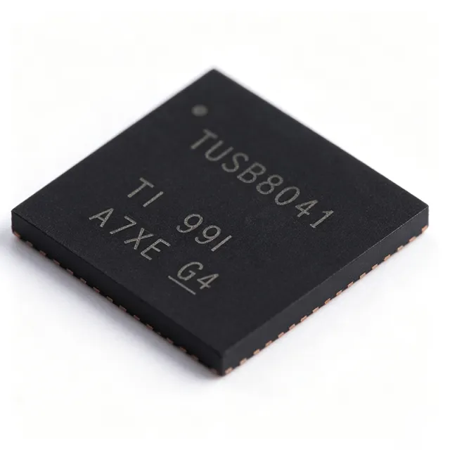
The Texas Instruments TUSB8041ARGCT is a 4-port SuperSpeed 5-Gbps USB 3.1 Gen1 hub controller in a 64-pin VQFN (RGC) 9x9 mm package with an exposed thermal pad. The device integrates four downstream USB ports that simultaneously support Low-Speed, Full-Speed, High-Speed, and SuperSpeed signaling, delivering up to 5 Gbps per downstream port while presenting a single upstream USB 3.1 Gen1 Type-A or Type-C interface to the host. A USB hub controller is an interface IC that multiplies a single upstream USB port into multiple downstream ports while preserving protocol compliance, port power switching, and per-port status reporting. Hubs occupy a fixed position in the USB device-class hierarchy between the host controller root hub and downstream peripherals. Modern SuperSpeed hubs additionally embed PHYs and link-training state machines so legacy USB 2.0 traffic and 5 Gbps SuperSpeed traffic are bridged transparently across the same physical connector stack. The TUSB8041ARGCT provides per-port battery-charging detection, downstream-port power-enable controls routed through GPIO, and over-current flag inputs that simplify USB Type-A VBUS switching designs. Configuration is achieved through pin-strap modes, OTP ROM, an external I2C EEPROM, or an I2C/SMBus slave interface for VID, PID, and custom-string descriptors. The integrated 1.1 V core LDO and 3.3 V I/O supply mean only a single external 3.3 V rail is required for the hub itself. Typical applications include desktop and laptop docking stations, retail POS terminals, industrial PCs, USB 3.0/3.1 port replicators, automotive infotainment hubs, and embedded systems that fan out a single Type-C upstream port into multiple USB Type-A ports. The -40C to +85C industrial temperature range supports deployment in factory automation and vehicle environments. When designing with the TUSB8041ARGCT, route the SuperSpeed differential pairs (USB3_TX/RX) for 85 ohm differential impedance with intra-pair length matching within 150 mil, and provide an external 24 MHz crystal with the datasheet-recommended load capacitors. Place the upstream port ESD protection array adjacent to the USB connector and verify the bulk-decoupling ESR budget against the 5V VBUS load step on hot-plug events. This page synthesizes distributor pricing from DigiKey and Arrow, cross-references the TUSB8041A 'A' revision orderability codes (RGC = tape-and-reel, RGT = tray), and provides drop-in alternatives plus design notes not collected in any single datasheet document.

견적 요청 문의하기
TUSB8041IPAPRQ1 - Automotive 4-Port USB 3.0 Hub | Texas Instruments
TUSB8041IPAPRQ1

TUSB8041IPAPRQ1 - Automotive 4-Port USB 3.0 Hub | Texas Instruments

The Texas Instruments TUSB8041IPAPRQ1 is an automotive-grade, four-port, SuperSpeed 5-Gbps USB 3.0 hub controller in a 64-pin HTQFP (PAP) 10x10 mm package with exposed thermal pad, qualified to AEC-Q100 standards and operating across -40C to +85C. It supports simultaneous SuperSpeed, Hi-Speed, Full-Speed and Low-Speed upstream connections while delivering full backward compatibility on every downstream port. A USB hub controller is a class of interface IC that aggregates one upstream USB port into multiple downstream ports, managing enumeration, power switching, transaction translation and battery-charging detection across every port. The TUSB8041 sits in a hierarchy of USB Type-C and USB-C hub ICs, which themselves belong to the broader interface ICs and connectivity category within mixed-signal semiconductors. The Q1 suffix designates AEC-Q100 qualification, meaning the device is engineered and tested for the temperature, vibration and reliability stresses of in-vehicle electronics such as infotainment head units, telematic control units and rear-seat entertainment modules. Key specifications include four downstream ports, integrated USB 2.0 hub with multi-translation support, configurable via I2C, SMBus, GPIO and pin straps, and 1.1V / 3.3V dual-rail operation. The PAP variant of the family uses the 64-HTQFP footprint (10 mm x 10 mm) and offers broad flexibility for USB Type-C deployments when paired with a downstream crosspoint switch or PD controller. Typical applications include automotive head-unit USB expansion, rear-seat USB charging hubs, telematic USB pass-through, factory-floor USB test rigs and embedded computing platforms that need multiple USB-3 connections from a single root port. Because the device supports per-port power switching via the USB specification and individual over-current flags, designers can implement ganged or individual port power policies directly through hardware strap settings. When evaluating USB-3 hub alternatives, confirm that any candidate supports simultaneous SuperSpeed on all four ports, matches the 64-HTQFP land pattern, retains the I2C/SMBus configuration interface and meets AEC-Q100 grade-2 or stricter temperature targets. Note that 3.3 V supply noise from upstream regulators must remain below the threshold documented in TI's USB-3 hub electrical spec section, otherwise link-training jitter on SuperSpeed pairs can rise substantially.

견적 요청 문의하기
TUSB8041IRGCT - 4-Port USB 3.0 Hub 5Gbps VQFN-64 | Texas Instruments
TUSB8041IRGCT

TUSB8041IRGCT - 4-Port USB 3.0 Hub 5Gbps VQFN-64 | Texas Instruments

The Texas Instruments TUSB8041IRGCT is a four-port SuperSpeed USB 3.0 hub controller delivering 5 Gbps per port, housed in a 64-pin VQFN (RGC, 9x9 mm) package and rated for -40C to +85C industrial operation. A USB 3.0 hub controller is an integrated circuit that fans a single upstream SuperSpeed USB link out to multiple downstream ports, handling enumeration, transaction translation, and power management transparently to the host. Hub controllers sit in the USB interconnect tier of the system I/O hierarchy: host controller -> hub controller -> downstream devices, bridging the gap between a PC or embedded host and the peripherals it must serve. The TUSB8041 supports USB 3.0 SuperSpeed (5 Gbps) operation on all four downstream ports while remaining backward compatible with USB 2.0 and USB 1.1 devices on the same ports. It provides GPIO, I2C, and SMBus interfaces for configuration and status monitoring, allowing designers to customize hub behavior, set port modes, and read fault status in embedded systems. The industrial temperature rating (-40C to +85C) of the TUSB8041I variant makes it suitable for deployments beyond office-climate conditions. Architecturally, the device integrates the SuperSpeed hub repeater, USB 2.0 hub engine, and configuration ROM/EEPROM loading logic in a single die. Configuration can be performed via an external serial EEPROM or through the SMBus/I2C host interface, eliminating external glue logic. Integrated charge-pump and linear regulators generate the internal core supply from a single 3.3 V rail, simplifying power tree design. Typical applications include docking stations, port replicators, industrial PC and HMI USB expansion, embedded computing boards, and test and measurement instrumentation that requires multiple robust SuperSpeed ports from one upstream connection. Design consideration: USB 3.0 is a multi-gigabit differential signaling standard, so the 90-ohm differential impedance routing, length matching, and AC-coupling capacitor placement for the SuperSpeed pairs dominate signal integrity; place the device close to both the upstream connector and EEPROM, and follow the layout guidelines in the manufacturer datasheet. This page synthesizes verified distributor data, drop-in alternatives, pricing tiers, and practical design notes not found in the manufacturer datasheet alone, with pricing references stated as of 2026-09-03.

견적 요청 문의하기
TUSB8041RGCR - 4-Port USB 3.0 Hub 5Gbps | Texas Instruments
TUSB8041RGCR

TUSB8041RGCR - 4-Port USB 3.0 Hub 5Gbps | Texas Instruments

The Texas Instruments TUSB8041RGCR is a four-port SuperSpeed USB 3.0 hub controller delivering 5-Gbps data rates per port, powered from dual 1.1V and 3.3V supplies and housed in a 64-pin VQFN (RGC) package measuring 9x9 mm with an exposed pad. A USB hub controller is an integrated circuit that fans out a single upstream USB connection into multiple downstream ports, handling enumeration, packet routing, and power management per the USB 3.0 specification. Within the system hierarchy it sits at the interface-IC layer, bridging the USB physical layer and the host controller of a computer, docking station, or embedded processor. Key features include four downstream SuperSpeed ports supporting 5 Gbps, backward compatibility with USB 2.0 full-speed and high-speed traffic, and configuration via GPIO, I2C, or SMBus interfaces for flexible SMBus-based platform integration. The device supports battery charging scenarios and standard hub power management, and TI offers both commercial (0C to 70C) and industrial (-40C to 85C) temperature grades in the same 64-pin RGC footprint. Architecturally, the TUSB8041 integrates the SuperSpeed repeater/retimer functions and hub transaction logic on a single die, using internal PLL-based clocking to regenerate the 5-Gbps link. The dual-rail 1.1V core / 3.3V I2V supply scheme reduces core power while maintaining signaling compliance, and the exposed-pad VQFN package provides low-inductance ground return for the high-speed differential pairs. Typical applications include PC motherboards and docking stations, monitors and displays with integrated USB hubs, industrial PCs requiring multiple USB 3.0 ports, and self-powered or bus-powered peripheral hubs. The 5-Gbps throughput makes it suitable for external storage, video capture, and camera aggregation. When designing with the TUSB8041, maintain 90-ohm differential impedance on the SuperSpeed pairs, keep them short and matched, and decouple both the 1.1V and 3.3V rails with low-ESR ceramics close to the pins. Configuration strapping or an I2C EEPROM must be present for non-default VID/PID settings. This page synthesizes distributor pricing, temperature-grade alternatives, and practical design notes not found in the manufacturer datasheet, verified as of 2026-09-03.

USD $4.05 문의하기
TUSB8043RGCT - 4-Port USB 3.1 Gen1 Hub Controller | Texas Instruments
TUSB8043RGCT

TUSB8043RGCT - 4-Port USB 3.1 Gen1 Hub Controller | Texas Instruments

The Texas Instruments TUSB8043RGCT is a 4-Port SuperSpeed USB 3.1 Gen1 hub controller supporting 5.0 Gbps signaling on downstream ports, housed in a 64-pin VQFN (RGC) 9x9 mm package. It integrates USB HID to I2C bridging, allowing host-side configuration of an attached EEPROM without an external bridge chip. The device supports full-speed, high-speed, and SuperSpeed USB operation across all four ports. A USB 3.1 hub is a connectivity expansion device that multiplies one upstream USB port into four downstream USB ports while maintaining protocol-aware traffic management. In the hierarchy of USB silicon, the TUSB8043 sits between USB 2.0 hubs (480 Mbps legacy) and USB 3.2 Gen2 (10 Gbps) hubs, serving the dominant consumer, docking-station, and embedded segment where 5 Gbps SuperSpeed is sufficient and power/area efficiency matter. Key features include per-port transaction translators (TTs) for full-/high-speed traffic, USB Battery Charging specification 1.2 support, integrated USB 2.0 PHY and SuperSpeed PHY per port, and configurable I2C/SMBus access through the HID endpoint. The device draws from a single 3.3 V supply rail and uses an external 25 MHz crystal, simplifying board layout. The RGC VQFN package exposes a thermal pad for heat spreading in sealed enclosures. Architecturally, the TUSB8043 implements a multi-RTL pipeline that schedules USB isochronous, interrupt, bulk, and control transfers independently per port, with split transactions across the 5 Gbps SuperSpeed lane for upstream traffic. Its hardware HID-to-I2C bridge maps vendor-specific USB control requests to I2C writes on the firmware-configured address, enabling platform designers to configure downstream peripherals from the host without an additional MCU. Typical applications include Thunderbolt and USB-C docking stations, industrial PCs and factory workstations, monitor bases with multiple USB peripherals, embedded computing platforms, point-of-sale terminals, and USB expansion cards. With USB-IF compliance built into the silicon, the TUSB8043 also powers medical imaging carts and test instrumentation where certified interoperability is mandatory. Designers should remember that downstream port power-enable and current-limit control require external TPS2041B/TPS2051B load switches; the TUSB8043 itself does not source VBUS. The 25 MHz reference must be a fundamental-mode crystal with ±50 ppm tolerance, and DP/DN traces on each downstream port require 90 Ω differential impedance matching to USB-IF compliance masks. This page aggregates distributor pricing, drop-in equivalents, and application-level design guidance drawn from the manufacturer datasheet and field reference designs, going well beyond a single-source product listing.

견적 요청 문의하기
TUSB9261-Q1 - USB 3.0 to SATA Bridge AEC-Q100 | TI
TUSB9261-Q1

TUSB9261-Q1 - USB 3.0 to SATA Bridge AEC-Q100 | TI

The Texas Instruments TUSB9261-Q1 is an automotive-qualified, ARM Cortex-M3 microcontroller-based USB 3.0 to Serial ATA (SATA) bridge delivered in a 64-pin HTQFP package rated for -40C to +85C operation. It provides the hardware and firmware needed to implement a USB Attached SCSI Protocol (UASP)-compliant mass storage device, bridging HDDs, SSDs, optical drives, and other SATA 1.5-Gbps or SATA 3.0-Gbps devices to a SuperSpeed USB 3.0 host. A bridge IC is a dedicated interface converter that sits between two different bus protocols and translates transactions between them. Within the interface IC hierarchy (bridge -> USB interface controller -> interface IC -> semiconductor), the TUSB9261-Q1 belongs to TI's second generation of SuperSpeed USB-to-SATA bridges, specifically qualified for automotive applications per AEC-Q100, with a device CDM ESD classification of Level C3 as the noted exception. Key features include an embedded ARM Cortex-M3 processor core running TI firmware for UASP compliance, native support for SATA 1.5-Gbps and 3.0-Gbps device classes, and USB 3.0 SuperSpeed 5-Gbps connectivity on the host side. UASP support delivers significantly higher command queuing efficiency than legacy BOT (Bulk-Only Transport), reducing latency and improving throughput with modern SSDs. Integrated PHYs reduce external component count and BOM cost. The Cortex-M3 architecture allows TI to update bridge firmware, adding features and fixing interoperability issues without hardware changes, which is valuable for long-lifecycle automotive programs. AEC-Q100 qualification supports infotainment, telematics, and diagnostic ports where USB-attached storage must survive automotive temperature and ESD environments. Typical applications include automotive infotainment USB storage ports, in-vehicle diagnostic data loggers with SSD storage, and external HDD/SSD docking designs requiring automotive grade qualification. Design consideration: this device is flash-based firmware dependent; plan for firmware update provisions (I2C/EEPROM boot) in the PCB layout, and observe the datasheet note regarding SATA pin swapping documented on the TI E2E forum before finalizing routing.

견적 요청 문의하기
TVP5146M2PFP - 10-bit NTSC/PAL/SECAM Video Decoder | TI HTQFP-80
TVP5146M2PFP

TVP5146M2PFP - 10-bit NTSC/PAL/SECAM Video Decoder | TI HTQFP-80

The Texas Instruments TVP5146M2PFP is a 10-bit high-quality single-chip digital video decoder that digitizes and decodes all popular baseband analog video formats - including NTSC, PAL, SECAM composite, S-Video, component RGB and YPbPr - into digital component video, housed in an 80-pin PowerPAD HTQFP package (12x12 mm). It integrates Macrovision detection, a 5-line adaptive comb filter, SCART support, and four 30 MSPS 10-bit ADC channels, replacing multiple discrete decoder/filter ICs in mainstream consumer video designs. A digital video decoder is a mixed-signal IC that converts legacy analog broadcast and consumer video signals into a digital YCbCr or RGB pixel stream for downstream processing by a scalar, encoder, SoC, or capture ASIC. Within the broader taxonomy of mixed-signal ICs, the TVP5146M2 belongs to the video decoder family, which sits below video processors and above simple video amplifiers in the signal-chain hierarchy. Multi-standard support (NTSC M/N/4.43, PAL B/G/H/I/M/N/60, SECAM) allows one hardware design to ship worldwide without regional BOM variants. Key differentiating specifications include four integrated 10-bit ADCs sampling at up to 30 MSPS, an integrated 5-line adaptive comb filter for superior chroma/luma separation, Macrovision copy-protection detection, and 12 analog front-end inputs that multiplex automatically - composite, S-Video, component YPbPr, RGB, and SCART - under software control via I2C. Programmable gain, clamp, and offset on each channel allow direct connection to consumer-grade video sources without external op-amps. Architecture is built around TI's analog front-end, 10-bit ADC array, comb filter, and digital formatter block. The decoder outputs 8/16-bit ITU-R BT.601/BT.656 or 20-bit ITU-R BT.1120 digital component video, and supports both 2x and 1x oversampling modes. An internal color-space converter generates YCbCr and RGB outputs simultaneously, reducing host CPU overhead and shortening time-to-market for set-top box, DVR, and capture-card designs. Typical applications include set-top boxes and DVRs decoding composite or component broadcast video, USB video capture cards capturing VHS/DVD or legacy consoles, video conferencing codecs, surveillance DVRs, and automotive rear-seat entertainment head units that digitize external composite sources. The wide input tolerance also suits broadcast monitor walls and medical imaging reference inputs. When laying out a PCB, allocate a solid ground plane beneath the PowerPAD and stitch the exposed pad with at least 9 thermal vias to the inner ground layer. Use 75 ohm-controlled-impedance routing on all analog video inputs to preserve 2T pulse response, and place anti-alias RC networks within 5 mm of each analog pin. Decouple both 1.8 V and 3.3 V rails with 0.1 uF X7R ceramics in parallel with 10 uF bulk capacitors at the supply pins. This page synthesizes distributor pricing from Mouser and DigiKey, drop-in same-package alternatives, and practical design notes (PCB layout, thermal pad, decoupling) not found in the manufacturer datasheet alone, giving engineers a one-stop reference for the TVP5146M2PFP.

견적 요청 문의하기
TVP5147M1PFPR - 10-bit NTSC/PAL/SECAM Video Decoder | TI HTQFP-80
TVP5147M1PFPR

TVP5147M1PFPR - 10-bit NTSC/PAL/SECAM Video Decoder | TI HTQFP-80

The Texas Instruments TVP5147M1PFPR is a 10-bit high-quality single-chip digital video decoder that digitizes and decodes NTSC, PAL, and SECAM analog composite, S-Video, and component YPbPr signals into digital component video (YCbCr 4:2:2), housed in an 80-pin HTQFP (PFP) PowerPAD package with 12x12 mm body. According to TI product page, it integrates two 10-bit ADCs, a 5-line adaptive comb filter, and Macrovision 1.x/2.x detection, providing a complete analog front-end plus decoder in a single device. What is a video decoder? A video decoder is a type of interface IC that converts analog baseband video signals (composite CVBS, Y/C, or YPbPr component) into digital ITU-R BT.656 or BT.601 video streams. Within the broader taxonomy, video decoders belong to encoders/decoders/converters in interface ICs, sitting between analog video sources (tuners, cameras, DVD players) and digital video processors (DSPs, SoCs, FPGAs). They are essential building blocks in LCD TV/Monitor designs where legacy analog video must be displayed on digital panels. The TVP5147M1's key differentiating features include a hardware Macrovision detection circuit (Macrovision 1.x and 2.x compliant), a 5-line adaptive comb filter for superior luminance/chrominance separation in NTSC/PAL, automatic gain control with peak/average modes, and TI's proprietary chroma transient improvement (CTI) and luminance peaking circuitry. The device supports ten analog input channels selected via I2C, programmable H/V sync outputs, VBI data slicing for teletext/closed caption, and outputs ITU-R BT.656, BT.601, or raw VBI data over an 8- or 16-bit parallel interface. A single 27 MHz reference clock serves all standard video formats. Architecturally, the TVP5147M1 combines two 10-bit, 30 MSPS ADCs with a programmable automatic gain control, a chroma demodulator with subcarrier PLL, a 5-line comb filter, and a digital output formatter. Analog supplies are 1.8 V (analog) and 3.3 V (I/O), while the digital core runs from an internally regulated 1.8 V supply. The HTQFP-80 PowerPAD package provides a thermal pad that must be soldered to a ground plane for adequate heat dissipation; PowerPAD operation lowers junction temperature and improves long-term reliability in always-on consumer equipment. Typical applications include LCD TV and LCD monitor analog video inputs, set-top boxes archiving analog broadcasts, digital video recorders (DVR), video capture cards for PCs, in-car rear-seat entertainment displays, and security DVR systems. The Macrovision detection makes it suitable for licensed playback equipment where copy protection circuitry is mandated by content owners. When designing with this device, ensure the PowerPAD is soldered to a continuous ground copper pour with multiple thermal vias to maximize heat flow. Use a 27 MHz crystal with low jitter (<50 ps RMS) to minimize pixel-clock jitter on the digital output, which directly impacts downstream display quality. Decouple the 1.8 V analog and 3.3 V I/O rails with 0.1 uF and 10 uF ceramic capacitors placed as close to the supply pins as practical. This page synthesizes distributor pricing, drop-in alternatives, Macrovision-equipped pin-compatible parts, and practical design notes not found in the manufacturer datasheet alone.

견적 요청 문의하기
TVP5150AM1IPBS - Ultra-Low Power NTSC/PAL/SECAM Video Decoder | TI
TVP5150AM1IPBS

TVP5150AM1IPBS - Ultra-Low Power NTSC/PAL/SECAM Video Decoder | TI

The Texas Instruments TVP5150AM1IPBS is an ultralow-power NTSC/PAL/SECAM video decoder that converts baseband analog video (composite, S-Video, or component Y/C) into 8-bit ITU-R BT.656 digital output. Housed in a 32-pin TQFP (PBS) 5x5 mm package, it integrates a high-speed 9-bit ADC, two composite or one S-Video input, and fully differential CMOS analog preprocessing channels with clamping and automatic gain control (AGC) for best signal-to-noise performance. What is a video decoder? A video decoder is a mixed-signal integrated circuit that digitizes analog broadcast video (NTSC, PAL, SECAM) and reformats it into a standard digital stream that downstream processors, image signal processors (ISPs), or video encoders can consume. In the broader taxonomy, the TVP5150AM1IPBS sits under video front-end ICs -> interface ICs -> integrated circuits, and historically it dominated mobile, surveillance, and set-top box designs where small footprint and low power were non-negotiable. Key features include a robust sync detector for non-standard and weak signals, Genlock/real-time control (RTC) output for synchronizing downstream encoders, complementary 4-line adaptive comb filtering for both luminance and chrominance paths, and a programmable chrominance trap filter. Per the TI datasheet, power consumption is typically below 150 mW, and the device operates from a 1.8 V core supply with a 3.3 V I/O supply via an integrated level shifter. Technically, the device uses a 9-bit pipelined ADC architecture, two fully differential analog preprocessing channels, and an on-chip PLL to generate the 27 MHz sampling clock from a 27 MHz crystal or external reference. The I2C interface is used for configuration of video standard, brightness, contrast, saturation, hue, and comb-filter enable, while the parallel 8-bit output uses the ITU-R BT.601 or BT.656 interface standard. Typical applications include handheld/personal video recorders, mobile phone video capture, portable media players, digital still cameras, automotive infotainment rear-seat displays, and CCTV/DVR surveillance front ends where composite CVBS must be digitized for compression ASICs or SoCs. When designing with this device, provide adequate bulk decoupling on both the 1.8 V (DVDD) and 3.3 V (IO_DVDD) rails and route the analog video inputs with controlled 75 ohm impedance to minimize reflections. The S-Video Y/C pair is preferred over CVBS for best comb-filter performance.

견적 요청 문의하기
TVP5150AM1IPBSR - Ultra-Low Power NTSC/PAL/SECAM Video Decoder | TI
TVP5150AM1IPBSR

TVP5150AM1IPBSR - Ultra-Low Power NTSC/PAL/SECAM Video Decoder | TI

The Texas Instruments TVP5150AM1IPBSR is an ultra-low-power NTSC/PAL/SECAM video decoder that converts analog composite or S-Video inputs to digital ITU-R BT.656 formatted output. It integrates a high-speed 9-bit ADC, supports two composite or one S-Video input, and is housed in a 32-pin TQFP (PBS) 5x5mm package. Operating from 1.65 V to 1.95 V analog and 1.65 V to 3.6 V digital supplies, the device consumes only 115 mW typical, making it ideal for portable and battery-powered imaging systems. What is a video decoder? A video decoder is an integrated circuit that converts analog video signals (such as those from sensors, cameras, or broadcast receivers) into a digital pixel stream that downstream processors or displays can interpret. Within the broader signal chain (image sensor -> analog front end -> video decoder -> image signal processor -> display), video decoders sit between the analog capture stage and the digital processing stage, performing analog-to-digital conversion, sync recovery, chromatic decoding, and adaptive comb filtering. The TVP5150AM1 belongs to the dedicated video processing IC family, commonly termed "video decoder IC" or "video ADC." Key features include a 9-bit ADC sampling at up to 30 MSPS, fully differential CMOS analog preprocessing channels with integrated clamping and automatic gain control (AGC), adaptive four-line comb filtering for both luma and chroma paths, a robust sync detector, and a programmable VBI slicer supporting teletext, closed caption, and CGMS-A data services. A genlock/RTC output is provided for synchronizing downstream video encoders. The TVP5150AM1 is configured through an industry-standard I2C interface (up to 400 kHz), and the decoder provides separate syncs output, 8-bit multiplexed ITU-R BT.656 output, and 16-bit YCbCr output formats. Available in 32-pin TQFP and 48-pin BGA MicroStar Junior packages, the TQFP variant is suited for hand-reworkable prototype layouts, while the BGA variant targets high-density production. Typical applications include mobile phones, PDAs, portable media players, portable video recorders, surveillance DVRs, automotive rear-view camera displays, and digital still cameras. AEC-Q100 qualification also enables use in automotive vision ECUs. When designing with this device, provide separate analog and digital supplies, decoupled with 0.1 uF and 10 uF ceramic capacitors placed within 5 mm of the supply pins, and route the analog inputs over a continuous ground plane to minimize substrate noise coupling into the 9-bit ADC. This page synthesizes cross-brand alternatives, ready-stock distributor tiers, and design notes beyond those in the manufacturer datasheet to accelerate part selection and downstream schematic capture.

견적 요청 문의하기
TVP5150AM1PBS - Ultralow-Power NTSC/PAL/SECAM Video Decoder | TI
TVP5150AM1PBS

TVP5150AM1PBS - Ultralow-Power NTSC/PAL/SECAM Video Decoder | TI

The Texas Instruments TVP5150AM1PBS is an ultralow-power NTSC/PAL/SECAM analog video decoder that converts baseband composite or S-Video inputs to 8-bit ITU-R BT.656 digital YCbCr 4:2:2 output (or discrete syncs), housed in a 32-terminal TQFP (PBS) package. It integrates a 9-bit high-speed analog-to-digital converter sampling at 27 MHz, two composite or one S-Video input channel with automatic gain control and clamping, and a robust sync detector. Operating from 1.65 V to 1.95 V (digital) and 1.65 V to 1.8 V (analog), it accepts NTSC (J, M, 4.43), PAL (B, D, G, H, I, M, N, Nc), and SECAM (B, D, G, K, K1, L) video standards. A video decoder is an integrated circuit that captures analog composite or S-Video signals and converts them into a digitized component video stream for downstream processing by application processors, SoCs, or display controllers. The device category hierarchy is: video decoder -> analog front-end -> interface IC -> semiconductor. Its role in a typical embedded vision system is to bridge analog cameras or legacy analog video sources (CVBS, Y/C) to modern digital processing pipelines, eliminating the need for external ADCs and sync separators while preserving signal integrity. Key features include a high-speed 9-bit ADC, fully differential CMOS analog preprocessing with AGC and clamping for best signal-to-noise performance, complementary 4-line adaptive comb filtering on both luminance and chrominance paths, Macrovision copy-protection support, and an ultralow-power architecture suited to portable designs. A Genlock/real-time control (RTC) output is generated for synchronizing downstream video encoders in multi-camera or PIP architectures. Technically, the TVP5150AM1 uses a differential analog front end that rejects common-mode noise and supports extended temperature operation from 0°C to 70°C in the PBS package variant. Its register-based I²C control interface exposes luminance, chrominance, hue, brightness, contrast, and sharpness adjustments to the host processor. Typical applications include portable media players, set-top boxes, digital video recorders, video capture cards, automotive infotainment rear-seat entertainment, IP cameras with analog CVBS input, and surveillance DVRs. The wide standard coverage and ultralow-power operation make it suitable for any embedded design that must decode legacy analog video. When designing with this part, pay attention to the I/O supply sequencing constraint: IO_DVDD must track the 1.8 V digital supply and must not be back-powered; an external power-on-reset (POR) or supply sequencing network may be required for multi-supply rails. Place the 27 MHz crystal or clock source within 5 mm of the XTAL pin and use a star-ground topology for the CVBS traces. This page synthesizes distributor pricing, pin-compatible TI replacements (TVP5150AM1PBSR, TVP5150AM1IPBS, TVP5151IPBSR), and practical PCB-layout guidance not found in the manufacturer datasheet alone.

견적 요청 문의하기
TVP5150PBS - Ultralow-Power NTSC/PAL Video Decoder, 32-TQFP
TVP5150PBS

TVP5150PBS - Ultralow-Power NTSC/PAL Video Decoder, 32-TQFP

The Texas Instruments TVP5150PBS is an ultralow-power NTSC/PAL video decoder housed in a 32-pin TQFP (PBS) package. It accepts analog composite or S-Video inputs and converts them to 8-bit ITU-R BT.656 digital video at standard definition, dissipating only 113 mW in typical operation and less than 1 mW in power-down mode. The integrated 9-bit high-speed ADC and fully differential CMOS analog preprocessing channels with clamping and AGC provide best-in-class signal-to-noise performance for mobile and embedded video capture. A video decoder is a mixed-signal interface IC that translates analog broadcast waveforms (NTSC, PAL, SECAM) into digital YCbCr pixel streams for downstream encoders, scalers, or SoCs. Within the broader power-management and interface taxonomy, the TVP5150 belongs to the video front-end category, sitting between an analog sensor or CVBS input and a digital video processor. Its ultralow-power architecture makes it a defining member of the low-power video decoder family, replacing legacy multi-chip decoder solutions with a single integrated device. Key features include support for NTSC (M, N, 4.43) and PAL (B, D, G, H, I, M, N) standards with ITU-R BT.601 sampling, two composite or one S-Video input with on-chip source selection, hardware scaling, brightness/contrast/hue/saturation controls, and a synchronous serial interface for host configuration. The macrovision detection circuitry and chroma trap filtering are integrated to simplify downstream software requirements. The TVP5150 uses a 27 MHz reference clock and produces ITU-R BT.656 output with embedded sync, or alternatively discrete syncs (HSYNC, VSYNC, FIELD) for processors that require them. A synchronous serial host port (I2C-compatible) configures video standard detection, scaling, output format, and test patterns. Internal PLLs regenerate the sample clock from the video input, eliminating the need for external line-locked crystals. Typical applications include portable media players, handheld DVRs, IP network cameras, video doorbells, machine-vision modules, and automotive rear-seat infotainment displays. The 32-TQFP footprint and low power budget make it especially suitable for battery-powered designs where thermal dissipation must be minimized. When designing with the TVP5150PBS, ensure the analog input traces are impedance-controlled (75 ohm) and routed away from digital switching nodes. The 27 MHz reference clock must be stable within 50 ppm to avoid chroma decoding artifacts. Decouple AVDD and DVDD separately with 0.1 uF and 10 uF ceramic capacitors placed within 5 mm of the supply pins. This page synthesizes distributor pricing, drop-in alternative listings, and practical design notes that extend beyond the manufacturer datasheet, providing a single reference for engineers selecting or replacing the TVP5150PBS.

견적 요청 문의하기
TVP5151IPBSR - Ultralow-Power NTSC/PAL/SECAM Video Decoder | TI
TVP5151IPBSR

TVP5151IPBSR - Ultralow-Power NTSC/PAL/SECAM Video Decoder | TI

The Texas Instruments TVP5151IPBSR is an ultralow-power NTSC/PAL/SECAM video decoder housed in a 32-pin TQFP (PBS) package measuring 5x5 mm. It accepts composite (CVBS) and S-Video analog inputs and converts them to 8-bit ITU-R BT.656 digital video with embedded syncs, or to 8-bit 4:2:2 with discrete syncs. The decoder supports NTSC (J, M, 4.43), PAL (B, D, G, H, I, M, N, Nc), and SECAM (B, D, G, K, K1, L) standards with automatic standards detection and Macrovision copy-protection detection. A video decoder is a mixed-signal integrated circuit that digitizes analog baseband video from cameras, set-top boxes, or playback devices so a digital processor, image signal processor, or display controller can consume the stream. Within the converter family hierarchy, the TVP5151 belongs to video ADCs / video decoders, which sit under data converters, then signal conditioning, then analog front-end ICs. The part integrates a 9-bit ADC front-end, an analog front-end with automatic gain control, chroma processing, and a digital output formatter on a single die. Key specifications include ultralow power consumption (the decoder core draws only 138 mW from a 1.7 V analog and 1.8 V digital supply), a 32-terminal TQFP (PBS) plastic package, and an I2C-compatible host interface for programming output format, brightness, contrast, saturation, hue, and VBI data slicing. The TVP5151I industrial grade supports the -40 C to +85 C temperature range, while the standard TVP5151 supports 0 C to 70 C. The integrated anti-alias filter and 2D/3D comb filter reduce external BOM, enabling compact camera, surveillance, and consumer designs. Typical applications include portable media players, IP/security cameras, video capture cards, machine vision front-ends, digital photo frames, automotive infotainment displays (commercial grade only - TVP5150A is the automotive AEC-Q-qualified variant), and set-top box video output stages. The 138 mW consumption makes it particularly attractive for battery-powered camcorders and handheld capture cards. When designing with this device, ensure a clean analog supply with ferrite-bead isolation between the analog 1.8 V rail and digital 1.8 V rail. Provide a stable 14.31818 MHz VCO reference for the decoder's internal timing recovery. Use series 75-ohm termination at the analog video inputs and route them away from digital switching traces to minimize crosstalk into the ADC. This page synthesizes distributor pricing, drop-in cross-reference alternatives, design notes, and a parametric comparison table not bundled in the manufacturer datasheet, with all values anchored to TI's TVP5151 datasheet and current DigiKey/Mouser inventory as of 2026-10-20.

견적 요청 문의하기
TVP5154AIPNP - 4-Ch Video Decoder 128-HTQFP | Texas Instruments
TVP5154AIPNP

TVP5154AIPNP - 4-Ch Video Decoder 128-HTQFP | Texas Instruments

The Texas Instruments TVP5154AIPNP is a 4-channel, low-power NTSC/PAL/SECAM video decoder with independent scalers, housed in a 128-pin HTQFP (PNP) PowerPAD package measuring 14x14 mm. Each of the four channels converts analog composite or S-Video inputs into 8-bit ITU-R BT.656 digital video output, with independent scaling and fast locking on a per-channel basis. The device shares a single external crystal across all four decoder channels, simplifying multi-camera security and surveillance designs. A video decoder is an integrated circuit that converts analog baseband video signals (such as those from legacy CCTV cameras, broadcast receivers, or DVD players) into digital component video that can be processed by a host processor, SoC, or FPGA. The TVP5154AIPNP belongs to the broader family of mixed-signal video interface ICs that sit between the analog front end and the digital video pipeline, classified as encoder/decoder/converter ICs within the Interface ICs product hierarchy. Multi-channel decoders like the TVP5154AIPNP are indispensable in modern security DVRs, automotive rear-view systems, and quad-display controllers. Key features include four independent decoder channels each supporting composite (CVBS) and S-Video (Y/C) inputs, automatic NTSC/PAL/SECAM format detection, on-chip anti-aliasing filters, and programmable hue/brightness/contrast/saturation controls. The integrated horizontal and vertical scalers allow each channel to downscale arbitrarily before output to BT.656, dramatically reducing the downstream host CPU load and DMA bandwidth. Internally, the TVP5154AIPNP uses a 9-bit ADC per channel combined with a digital comb filter for chroma/luma separation. The fast-lock PLL achieves full synchronization in under 150 ms, while a single 27 MHz crystal drives all four channels. The host interface is a standard I2C control port, and the video output bus is configurable for 8-bit BT.656 or discrete syncs. Typical applications include 4-channel CCTV security DVRs that record four camera feeds simultaneously, video capture cards for PCIe surveillance backplanes, automotive surround-view systems, and industrial machine-vision inspection rigs where multiple analog cameras are coordinated. Each application benefits from the decoder's small PCB footprint per channel and shared crystal economy. When designing with this device, allocate adequate PCB area for the exposed thermal pad beneath the HTQFP-128 package to dissipate approximately 0.6 W of total power across all four active channels. Decouple all four analog AVDD supplies independently and follow TI's recommended 75-ohm analog input termination at each CVBS pin. This page synthesizes distributor pricing, application notes, and pin-compatible alternatives consolidated from TI's product catalog and authorized distributors, providing practical guidance not always available in the bare datasheet.

견적 요청 문의하기
TVP5154AIPNPR - 4-Ch PAL/NTSC/SECAM Video Decoder | TI
TVP5154AIPNPR

TVP5154AIPNPR - 4-Ch PAL/NTSC/SECAM Video Decoder | TI

The Texas Instruments TVP5154AIPNPR is a 4-channel, low-power NTSC/PAL/SECAM video decoder with independent scalers and fast lock, housed in a 128-pin HTQFP (PNP) PowerPAD package measuring 14x14 mm. Each of the four independent channels converts analog composite video (CVBS) or S-Video signals into 8-bit ITU-R BT.656 digital output, with discrete syncs also available. The device operates from a 1.8 V core supply and a 3.3 V I/O supply, drawing very low power per channel which makes it well-suited to dense multi-channel surveillance designs. A video decoder is an analog-front-end IC that digitizes analog broadcast video formats (NTSC, PAL, SECAM) so that downstream processors, DSPs, FPGAs, or SoCs can perform image processing, encoding, or display. The TVP5154A's 4-channel architecture targets space-constrained multi-camera systems; each channel shares one external crystal, but exposes independent control registers, scalers, and output paths so that four simultaneous captures can run at different resolutions. Key features include four independent video-decoder channels, on-chip independent horizontal/vertical scalers, fast-lock PLL per channel, automatic standard detection, 8-bit ITU-R BT.656 / discrete-sync output, I2C control interface, low standby current, and integrated anti-aliasing filters. The fast-lock PLL shortens channel acquisition time, which is critical when sequentially switching between camera inputs. Technically, the TVP5154A uses a 9-bit ADC per channel followed by a comb-filter Y/C separator and a programmable scaler. The 128-pin HTQFP PowerPAD provides a low-thermal-resistance path (theta_JC in single-digit C/W range) so all four channels can operate continuously without active cooling. The device is qualified to the industrial temperature range (-40C to +85C). Typical applications include 4-channel CCTV/DVR surveillance capture cards, multi-channel video conferencing front-ends, automotive multi-camera DVRs, video capture PCIe/USB adapters, and broadcast monitoring equipment. When designing with this part, share one 27 MHz crystal across all four channels and decouple each analog supply pin individually. Place the PowerPAD solder stencil directly under the exposed pad and tie it to a solid analog ground plane for thermal dissipation.

견적 요청 문의하기
TVP5158IPNPR - 4Ch NTSC/PAL Video Decoder, 128-HTQFP | Texas Instruments
TVP5158IPNPR

TVP5158IPNPR - 4Ch NTSC/PAL Video Decoder, 128-HTQFP | Texas Instruments

The Texas Instruments TVP5158IPNPR is a four-channel high-quality NTSC/PAL video decoder that digitizes and decodes all popular base-band analog video formats into digital video output. Each of the four channels integrates a 10-bit 27-MSPS analog-to-digital converter (ADC) preceded by an analog input conditioning circuit that clamps the input to a reference and applies anti-alias filtering. The device is offered in a 128-pin HTQFP (PNP) package measuring 14x14 mm with an exposed thermal pad, targeting multi-channel security and machine-vision applications. A video decoder is a mixed-signal integrated circuit that converts analog composite video signals (such as those from CCTV cameras or legacy broadcast outputs) into a digital component video stream for downstream processing by a host processor, SoC, or DSP. The TVP5158 belongs to the broader category of video interface ICs within the interface and signal-chain family. It supports NTSC (J, M, 4.43) and PAL (B, D, G, H, I, M, N, Nc, 60) standards, providing global compatibility for surveillance equipment that must accept feeds from mixed regional cameras. Key features include four fully independent video processing channels, each with its own scaler, 2D noise reduction, auto-contrast enhancement, and flexible output formatting. Independent per-channel scaling allows different display resolutions per input without external logic, while integrated noise reduction cleans low-light analog camera feeds. An I²C control interface manages all programming. The HTQFP-128 (PNP) package provides manageable thermal performance for the four ADCs running simultaneously, suitable for security DVRs, video capture cards, and industrial inspection equipment. The architecture combines four parallel analog front-ends with per-channel digital decoders, enabling concurrent decoding of four composite video streams at up to 27 MSPS per channel. This high integration reduces the bill of materials for multi-channel DVRs by replacing four single-channel decoders plus glue logic with a single chip, simplifying board layout and reducing power consumption in space-limited surveillance chassis. Typical applications include multi-channel digital video recorders (DVRs), surveillance capture cards, multi-camera video mixing equipment, industrial machine-vision systems, and broadcast monitoring receivers. Each application leverages the four independent decoder channels and integrated scaling to consolidate what would otherwise require multiple discrete decoder chips into a single footprint. Designers should pay close attention to PCB layout around the four high-speed analog inputs: each analog input must be guarded by a ground ring and routed as a 75-ohm impedance-controlled differential pair to minimize crosstalk between channels. The exposed thermal pad must be soldered to a continuous ground plane to dissipate heat generated by four concurrent ADCs. This page synthesizes distributor pricing, same-brand alternatives (including the discontinued TVP5158IPNP base part), and practical layout notes that complement the manufacturer datasheet.

견적 요청 문의하기
TVP5160PNP - NTSC/PAL/SECAM 10-Bit Video Decoder HTQFP-128 | TI
TVP5160PNP

TVP5160PNP - NTSC/PAL/SECAM 10-Bit Video Decoder HTQFP-128 | TI

The Texas Instruments TVP5160PNP is a high-quality digital video decoder that digitizes and decodes all popular baseband analog video formats into digital component video, integrating two 11-bit 60-MSPS analog-to-digital converters with analog preprocessors, fixed RGB-to-YUV color space conversion, and Macrovision detection. Housed in a 128-pin HTQFP (PNP) package measuring 14x14 mm, the device supports NTSC (J, M, 4.43), PAL (B, D, G, H, I, M, N, Nc, 60) and SECAM (B, D, G, K, K1, L) composite and S-Video inputs as well as component YPbPr and RGB (SCART) signals. A video decoder is an analog front-end IC that converts legacy analog video waveforms - originally designed for CRT displays - into digital YCbCr component streams for downstream processing by display controllers, scalar ASICs, video processors, or application processors. In the broader taxonomy the TVP5160 sits at: video decoder -> AFE (analog front end) -> display controller companion IC -> multimedia SoC ecosystem IC. Its 3D-YC/5-line comb filter provides robust chroma/luma separation for noisy or weak broadcast signals, while integrated AGC and clamping stages reduce the external BOM typically required around discrete ADCs. Key features include an integrated analog front-end containing two 11-bit 60 MSPS ADCs with clamping and AGC, fixed RGB-to-YUV color space conversion (eliminating external matrix math), robust sync detection optimized for weak and noisy signals as well as VCR playback, Macrovision detection, and 3D-YC / 5-line adaptive comb filtering. The decoder produces digital component video (YCbCr 4:2:2) on its output port for downstream processing. Operating voltage spans 3.0V to 3.6V (3.3V typical) with typical power dissipation of 904 mW. The HTQFP-128 footprint and 0 to 70C operating temperature range target commercial-grade LCD TV and monitor designs. Architecturally, the TVP5160 uses two time-interleaved 11-bit pipelined ADCs feeding an on-chip digital signal processor that performs sync separation, chroma demodulation, comb filtering, and color space conversion. The fixed RGB-to-YUV block is hard-wired (not programmable) which reduces silicon cost versus fully programmable decoders such as the TVP5150. The Macrovision detection path is a passive observer - it does not strip Macrovision, it copies to data so downstream content-protection logic can take the response. Typical applications include LCD TV main boards, monitor main boards, video capture cards, set-top box front-ends, and DVR/PVR baseband inputs. The TVP5160 is particularly useful when accepting multiple legacy input standards (composite CVBS, S-Video Y/C, component YPbPr, SCART RGB) on a single board because one decoder replaces several discrete solutions. The Macrovision detection path also enables DRM-aware DVR designs. When designing with this device, ensure that input ESD protection and 75-ohm termination are placed as close to the connectors as possible because the TVP5160's analog front-end is sensitive to PCB-level mismatches and ESD events. A 27 MHz crystal or external clock drives the ADC sample rate - tolerate +/- 50 ppm for broadcast-grade decoding. This page synthesizes distributor pricing, drop-in alternatives and practical design notes not found in the manufacturer datasheet, enabling a faster engineering decision for LCD TV and monitor main-board designs.

견적 요청 문의하기
TXB0104-Q1 - 4-Bit Auto-Direction Level Translator | TI
TXB0104-Q1

TXB0104-Q1 - 4-Bit Auto-Direction Level Translator | TI

The Texas Instruments TXB0104-Q1 is an automotive-grade 4-bit bidirectional voltage-level translator with automatic direction sensing and +/-15 kV ESD protection, available in a 14-pin TSSOP (PW) package. It translates between two independent supply rails: the A port tracks VCCA from 1.2 V to 3.6 V, while the B port tracks VCCB from 1.65 V to 5.5 V, enabling any-to-any translation between 1.2 V, 1.8 V, 2.5 V, 3.3 V and 5 V logic domains. A voltage-level translator is a logic-family device that allows integrated circuits operating at different supply voltages on the same PCB to exchange digital signals safely. Within the power-and-signal-management hierarchy, it sits alongside buffers and bus switches as a fundamental interface IC, preventing overvoltage damage and ensuring valid logic thresholds between low-voltage MCUs, FPGAs, and 5 V peripherals. Key features include auto-direction sensing, which eliminates the DIR control pins required by '245-style translators, a data rate of up to 100 Mbps, and VCC isolation: when either supply is at GND, all I/O enters Hi-Z. The AEC-Q100-qualified TXB0104-Q1 also carries +/-15 kV HBM ESD protection, exceeding the standard JESD ratings cited in the TI datasheet family. Architecturally, the TXB0104 uses a self-directed, edge-rate-driven one-shot scheme that detects the direction of each transition and briefly strengthens the opposite driver, allowing it to drive 4 channels in either direction without software intervention. The OE pin three-states all outputs for power sequencing and bus isolation. Typical applications include SPI and UART level conversion between 3.3 V MCUs and 5 V peripherals, GPIO expansion in automotive body and infotainment modules, and mixed-voltage FPGA I/O. Note that the push-pull architecture is not recommended for open-drain buses such as I2C or 1-Wire; use the TXS0104E-Q1 for those. Design consideration: keep unloaded outputs low-impedance driven or grounded, since the auto-direction circuitry can oscillate on lightly loaded or capacitively large nets; series resistors above 25 k-ohm are not supported. This page adds value beyond the TI datasheet by synthesizing distributor availability, drop-in alternatives (NXP NTS0304E, ADI ADG3304), and practical design notes for automotive level-shifter selection.

견적 요청 문의하기
TXB0104D - 4-Bit Bidirectional Level Translator, 100Mbps | TI
TXB0104D

TXB0104D - 4-Bit Bidirectional Level Translator, 100Mbps | TI

The Texas Instruments TXB0104D is a 4-bit bidirectional voltage-level translator with automatic direction sensing, delivering up to 100 Mbps data rates in a 14-pin SOIC (D) package, with VCCA from 1.2V to 3.6V and VCCB from 1.65V to 5.5V plus +/-15 kV ESD protection. A voltage-level translator (also called a level shifter) is a logic IC that interfaces digital circuits operating at different supply voltages, allowing a 1.8V microcontroller to safely communicate with a 3.3V or 5V peripheral. Level translators sit within the broader logic IC family, alongside buffers, transceivers, and bus switches, and are a fundamental part of system power-management and signal-chain design wherever mixed-voltage domains coexist. Key features of the TXB0104D include fully automatic direction sensing that eliminates the direction-control pin required by conventional transceivers, universal translation among 1.2V, 1.5V, 1.8V, 2.5V, 3.3V, and 5V nodes, and a 100 Mbps maximum data rate that supports fast embedded buses. An active-high OE input tri-states all eight I/Os when low, providing board-level power sequencing isolation. Architecturally, the TXB family uses two separate configurable power-supply rails: port A tracks VCCA and port B tracks VCCB. Internal one-shot circuits sense edges and briefly drive stronger pull-up/pull-down transistors, while a 4 kOhm series switch holds the level in static conditions. This push-pull CMOS design requires neither pull-up resistors nor direction control, but it does mean the TXB0104 is suited to push-pull CMOS outputs only, not open-drain buses unless replaced by the TXS family. Typical applications include MCU-to-peripheral interfacing across mixed voltage domains, SPI and UART signal translation, and general-purpose 1.2V-to-5V logic bridging in industrial and consumer systems. The -40C to +85C operating range covers most commercial and industrial environments. Design consideration: keep VCCA lower than or equal to VCCB, and remember the weak static drive (about 4 kOhm) cannot handle heavy loads, long wires, or pull-up resistors below about 50 kOhm. This page synthesizes verified distributor data, drop-in alternative analysis, and practical design notes not found in the manufacturer datasheet alone.

견적 요청 문의하기
TXB0104RUTR - 4-Bit Bidirectional Level Shifter | Texas Instruments
TXB0104RUTR

TXB0104RUTR - 4-Bit Bidirectional Level Shifter | Texas Instruments

The Texas Instruments TXB0104RUTR is a 4-bit bidirectional voltage-level translator with automatic direction sensing and ±15-kV ESD protection (Human Body Model), housed in a 12-pin UQFN (RUT) package measuring 1.7 mm x 2.0 mm. It translates signals between a low-voltage A port operating from 1.2 V to 3.6 V and a higher-voltage B port from 1.65 V to 5.5 V (VCCA <= VCCB), supporting data rates up to 100 Mbps. A voltage-level translator, also called a level shifter, is an integrated circuit in the logic-translation family that enables communication between digital devices operating at different supply voltages. In mixed-voltage systems, a 1.8 V or 3.3 V MCU may need to interface with 5 V peripherals; translators convert logic levels bidirectionally while protecting low-voltage silicon. The TXB0104 belongs to the auto-direction-sensing translator family, eliminating direction-control pins and simplifying both PCB design and firmware. Key features include per-channel automatic direction sensing, ±15-kV HBM ESD protection on all pins, tri-state outputs with an output-enable (OE) pin for bus isolation, and an operating temperature range of -40C to +85C. Low quiescent current and the tiny UQFN footprint suit space-constrained portable designs. Architecturally, the TXB0104 uses a one-shot edge accelerator that speeds rising and falling edges, enabling 100 Mbps operation with low static power. The A port tracks VCCA and the B port tracks VCCB. Partial power-down via OE and Ioff-style isolation make it suitable for hot-insertion environments. Typical applications include SPI, UART, and push-pull GPIO level shifting between MCUs, sensors, SIM card and SD card interfaces, and memory peripherals in mobile, industrial, and consumer products. The push-pull driver topology is not recommended for open-drain buses such as I2C or 1-Wire, as confirmed in TI E2E forum threads. Design tip: power VCCA before VCCB, place 0.1 uF bypass capacitors close to both supply pins, and use the OE pin for sequencing. For open-drain buses, consider TXS0104E instead.

견적 요청 문의하기
TXB0104W-Q1 - 4-Bit Auto-Direction Level Translator | Texas Instruments
TXB0104W-Q1

TXB0104W-Q1 - 4-Bit Auto-Direction Level Translator | Texas Instruments

The Texas Instruments TXB0104W-Q1 is an automotive-grade 4-bit bidirectional voltage-level translator with automatic direction sensing, rated for data rates up to 100 Mbps and protected by +/-15 kV IEC ESD protection on the I/O pins, housed in a 12-pin UQFN (RUT) package. Qualified per AEC-Q100 for automotive applications, the W variant supports a VCCA supply range of 1.1 V to 3.6 V and a VCCB range up to 3.6 V, translating between logic families such as 1.2 V, 1.8 V, 2.5 V, and 3.3 V rails. A voltage-level translator is a member of the logic IC family (voltage-level translator -> logic IC -> integrated circuit) that allows two circuit domains operating at different supply voltages to exchange digital signals safely. On mixed-voltage PCBs - for example, a 1.8 V microcontroller talking to a 3.3 V sensor - the translator isolates the rails while preserving logic polarity and timing, preventing overvoltage damage and logic-level misreads. Key features of the TXB0104W-Q1 include automatic direction sensing that eliminates DIR control pins, push-pull topology optimization delivering 100 Mbps throughput, and a compact 12-pin UQFN footprint of approximately 2 mm x 2 mm that saves board area. The +/-15 kV ESD rating (IEC) on the I/O ports adds robustness in harsh automotive electrical environments. According to TI product data, the device uses two separate configurable power-supply rails; the A port tracks VCCA and the B port tracks VCCB. Architecturally, the TXB family uses a two-transistor output driver with an integrated one-shot edge-rate accelerator on each side, giving fast transition times for push-pull CMOS signals. This makes it well suited to SPI, UART, and general-purpose push-pull GPIO translation. Note that, as TI applications guidance states, the TXB architecture is not recommended for open-drain buses such as I2C or 1-Wire, where the internal drivers contend with external pull-ups. Typical applications include automotive body electronics and gateways translating between 1.8 V SoC GPIO and 3.3 V peripherals, infotainment and display module signal interfaces, and industrial control modules requiring AEC-Q100 qualified components. Design tip: keep VCCA ramps before or after VCCB within datasheet sequencing guidance, and place the two 0.1 uF decoupling capacitors directly at the VCCA and VCCB pins; the auto-direction sensing requires push-pull sources on both sides to function reliably. This page synthesizes distributor pricing tiers, verified drop-in alternatives from TI cross-reference discussions, and practical design notes not found in the manufacturer datasheet.

견적 요청 문의하기
TXB0104YZTR - 4-Bit Auto-Direction Level Translator | TI
TXB0104YZTR

TXB0104YZTR - 4-Bit Auto-Direction Level Translator | TI

The Texas Instruments TXB0104YZTR is a 4-bit bidirectional voltage-level translator with automatic direction sensing, supporting 1.2V to 3.6V on the A port and 1.65V to 5.5V on the B port at data rates up to 100 Mbps, housed in a 12-ball DSBGA (YZT) package measuring 1.9 mm x 1.4 mm with +/-15 kV ESD protection. A voltage-level translator is a logic-interface device that allows integrated circuits operating at different supply voltages - for example a 1.8V microcontroller and a 5V sensor - to exchange digital signals reliably. Within the power-management and interface hierarchy, level translators sit between logic families such as CMOS and TTL, complementing buffers, bus switches, and transceivers in the broader signal-chain category. Without translation, low-voltage logic can be damaged by higher-voltage inputs or fail to meet higher-voltage logic thresholds. Key features of the TXB0104 include its two separate configurable power-supply rails (VCCA tracks the A port, VCCB tracks the B port, with VCCA <= VCCB), auto-direction sensing that eliminates direction-control pins, a maximum propagation delay of 13.7 ns, and 4 kV (HBM) class robustness supplemented by +/-15 kV IEC ESD protection on the I/O lines. The TXB architecture uses a mixed-charge pump output driver that pushes data in either direction without OE-based handshaking. Technically, the device derives its drive from a 4 kOhm output stage optimized for lightly loaded, point-to-point CMOS links; it is not a bus-holder for heavily capacitive or high-fanout loads. The 0.5 mm ball pitch and wafer-scale DSBGA packaging minimize board area, making it attractive for dense portable designs. The output enable (OE) pin tri-states all channels for power-aware sequencing. Typical applications include translating I2C-adjacent push-pull buses, SPI and UART links between 1.8V MCUs and 3.3V or 5V peripherals, SD-card interfaces, and general-purpose GPIO bridging in industrial and consumer systems. A key design consideration: avoid capacitive loads above roughly 30 pF and pull-up/pull-down resistors below about 25 kOhm, because the auto-direction scheme relies on one side driving the line; contested drivers cause bus contention. This page synthesizes distributor pricing, verified specifications, and practical design guidance for the TXB0104YZTR beyond what any single datasheet page provides.

견적 요청 문의하기
TXB0108PWR - 8-Bit Bidirectional Level Shifter 100Mbps | TI
TXB0108PWR

TXB0108PWR - 8-Bit Bidirectional Level Shifter 100Mbps | TI

The Texas Instruments TXB0108PWR is an 8-bit bidirectional voltage-level translator with auto-direction sensing and +/-15-kV ESD protection, housed in a 20-pin TSSOP (PW) package. It translates signals between a 1.2V to 3.6V A port and a 1.65V to 5.5V B port (VCCA <= VCCB), with data rates up to 100 Mbps, making it ideal for mixed-voltage digital systems. A voltage-level translator is a logic IC that enables communication between devices operating at different supply voltages, such as a 1.8V microcontroller and a 3.3V or 5V peripheral. It sits in the hierarchy of logic ICs under level shifters (translators), which are essential in multi-voltage digital systems alongside buffers and bus transceivers. The TXB0108PWR uses auto-direction sensing, eliminating the need for a direction control pin and reducing firmware complexity. Key features include auto-direction sensing, +/-15-kV ESD protection (HBM), a 100 Mbps maximum data rate, and a VCC isolation feature: if either VCC input is at GND, all outputs enter the high-impedance state, enabling partial-power-down operation with Ioff support. The device operates from -40C to +85C. Technically, the TXB0108 uses a one-shot architecture that accelerates low-to-high transitions to achieve 100 Mbps. It is designed for push-pull (totem-pole) CMOS drivers only; for open-drain buses such as I2C, TI recommends the TXS0108E. Output drive is intentionally weak (internal 4 kOhm series resistors), so heavy capacitive loads above ~70 pF reduce achievable speed. Typical applications include 1.8V-to-3.3V microcontroller-to-sensor interfaces, SD card level shifting, UART/SPI signal translation, and FPGA configuration buses. The 100 Mbps capability suits high-speed SPI and UART links. Design tip: ensure VCCA <= VCCB, drive all eight channels push-pull, and place 0.1uF decoupling capacitors close to both VCCA and VCCB pins with short traces for signal integrity.

견적 요청 문의하기
TXB0108QPWRQ1 - 8-Bit Auto-Direction Level Translator | TI
TXB0108QPWRQ1

TXB0108QPWRQ1 - 8-Bit Auto-Direction Level Translator | TI

The Texas Instruments TXB0108QPWRQ1 is an automotive-qualified (AEC-Q100) 8-bit bidirectional voltage-level translator with auto-direction sensing and ±15kV ESD protection, packaged in a 20-pin TSSOP (PW). Port A supports 1.2V to 3.6V supplies while Port B supports 1.65V to 5.5V, enabling translation between any two logic rails in these ranges. A voltage-level translator (also called a logic level shifter) is an interface IC that enables digital devices operating on different supply rails - such as a 1.8V microcontroller and a 5V peripheral - to communicate reliably. Translators sit within the broader logic IC family, under interface and signal-conversion devices, and are essential wherever mixed-voltage systems coexist on one board. Key features include auto-direction sensing that eliminates the need for a direction-control pin, an output-enable (OE) input that places all I/O in Hi-Z when low, and ±15kV IEC ESD protection on I/O pins. The TXB0108-Q1 uses TI TXB-type push-pull architecture, delivering symmetric drive on both ports without external pull-up or pull-down resistors, and supports data rates up to 100 Mbps for 1.2V to 3.6V translation per the datasheet. The device operates from -40C to +125C (AEC-Q100 Grade 1), making it suitable for harsh automotive environments. Its TSSOP-20 package is standard, easy to assemble, and compatible with the commercial TXB0108PWR footprint for design reuse. Typical applications include automotive infotainment and cluster modules interfacing 3.3V MCUs with 5V sensors, mixed-voltage SPI/I2C-style GPIO expansion, industrial control modules, and portable mixed-signal systems bridging 1.8V and 5V rails. Design note: the TXB architecture has relatively weak output drive (not intended for bus-holding or heavy loads); avoid using it for I2C open-drain buses - the TXS family is a better fit. Pull OE low during power sequencing to prevent bus contention.

견적 요청 문의하기