제품 (39,000+)

EP1C6Q240C6N Cyclone FPGA 185 I/O 240-Pin | Intel
EP1C6Q240C6N

EP1C6Q240C6N Cyclone FPGA 185 I/O 240-Pin | Intel

The Intel (Altera) EP1C6Q240C6N is a Cyclone® I field-programmable gate array (FPGA) containing 5,980 logic elements, 92,160 RAM bits, 2 PLLs, and 185 user I/Os, packaged in a 240-pin BFQFP/PQFP. This -6 speed-grade commercial device accepts a 1.5 V core supply and supports multiple I/O voltages, making it a practical mid-density programmable logic choice for control, interface, and signal-processing applications. An FPGA is an integrated circuit whose logic fabric can be configured after manufacturing using a hardware description language. Unlike fixed-function ASICs, FPGAs allow designers to implement custom digital logic in days and to update functionality in the field. The EP1C6Q240C6N sits in the hierarchy FPGA → programmable logic device → embedded semiconductor. It is used when an MCU does not have enough parallel I/O or when custom, high-speed logic must be implemented without the non-recurring expense of a custom chip. Key features of the EP1C6Q240C6N include 5,980 logic elements organized as 598 LABs, 20 M4K RAM blocks giving 92,160 total RAM bits, two PLLs, and 185 general-purpose user I/O pins. The package is a 240-pin BFQFP with a commercial operating range of 0°C to 85°C. The N suffix indicates lead-free, RoHS-compliant packaging. These resources support state machines, datapaths, soft-core processors, and parallel bus interfaces while the PLLs enable clock multiplication and phase alignment. The Cyclone I architecture separates the 1.5 V VCCINT core supply from the I/O supply, allowing each I/O bank to interface to 1.5 V, 1.8 V, 2.5 V, or 3.3 V logic. The fabric is SRAM-based, so the device must be configured from an external source, such as an Altera EPCS configuration device or a JTAG download. The -6 speed grade is the fastest standard commercial grade available in this family, providing lower propagation delays and higher achievable clock rates than -7 or -8 variants. Typical applications include industrial motor-control logic, PLC I/O expansion, test-and-measurement interface boards, video capture preprocessing, and communication bridging between processor buses. The 185 user I/Os are especially valuable when many parallel inputs and outputs must be monitored or controlled at deterministic timing. When designing with this device, plan for configuration storage and ensure all I/O bank voltages are connected according to the standards you use. The 1.5 V core should be adequately decoupled, and the power sequence should respect VCCINT and VCCIO requirements described in the Cyclone FPGA family data sheet. This page combines distributor pricing, verified availability, drop-in family alternatives, and design guidance that is not repeated in the manufacturer datasheet, giving engineers a convenient cross-reference for lifecycle and procurement decisions.

견적 요청 문의하기
EP1C6Q240C7 - Cyclone FPGA 5,980 LE, 92Kb RAM | Intel
EP1C6Q240C7

EP1C6Q240C7 - Cyclone FPGA 5,980 LE, 92Kb RAM | Intel

The Intel (Altera) EP1C6Q240C7 is a Cyclone I field-programmable gate array (FPGA) with 5,980 logic elements, 92,160 RAM bits, and 185 user I/Os, supplied in a 240-pin BFQFP package. It is a commercial-temperature, speed-grade 7 member of the low-cost Cyclone family, historically used in communication, industrial, and test equipment where configurable digital logic is required. An FPGA is an integrated circuit whose logic fabric can be configured after manufacturing. In the device hierarchy, an FPGA belongs to programmable logic devices and sits above discrete glue logic in design flexibility. The Cyclone I FPGA is SRAM-based, so it must load a configuration bitstream from an external configuration device, a host processor, or a JTAG cable at power-up. Unlike an ASIC, the EP1C6Q240C7 can be reprogrammed in-system, enabling late design changes, protocol updates, and shorter development schedules for medium-volume boards. Key features visible in verified distributor data include 5,980 logic elements, 598 logic array blocks, 92,160 total RAM bits, and 185 user I/O pins. The core logic is fabricated on a 130 nm process and operates from a 1.5 V supply, helping reduce dynamic power compared with older 2.5 V FPGAs. The 240-pin BFQFP package provides a manageable quad flat pack layout for cost-sensitive boards and manual or reflow assembly. The device architecture consists of logic elements grouped into LABs, embedded memory blocks for distributed buffering, and programmable interconnect that connects I/O pins to the core. With 598 LABs, designers can implement counters, state machines, decoders, small soft processors, and parallel bus interfaces. The 92,160 RAM bits support FIFOs, small packet buffers, and register files without adding external SRAM. The 185 user I/Os allow a high pin count for parallel busses and chip-to-chip interfaces. Typical applications include industrial controller I/O expansion, protocol bridging, data acquisition front ends, custom video timing generation, and FPGA prototyping. Because the part is an SRAM FPGA, it is particularly useful when the exact logic function is still evolving or when the same board must support multiple interface standards by changing only the configuration bitstream. One important design consideration is that the core requires a clean 1.5 V supply and a valid configuration source before user I/O can operate. Designers must handle power-up sequencing, strap the mode-select pins for the intended configuration scheme, and provide a configuration clock to the EPCS or download cable. Unused I/O pins should be assigned as inputs with weak pull-ups or driven to defined levels in the Quartus project to avoid floating nodes. This page synthesizes distributor stock signals, drop-in Intel/Altera family alternatives, comparison data, and practical design notes that are not all found in the brief distributor snippets. It is intended to help engineers quickly evaluate EP1C6Q240C7 for legacy FPGA designs and define the fastest safe migration path within the same 240-pin package.

견적 요청 문의하기
EP1C6Q240C7N - Cyclone FPGA, 5980 LE, QFP-240 | Intel
EP1C6Q240C7N

EP1C6Q240C7N - Cyclone FPGA, 5980 LE, QFP-240 | Intel

The Intel EP1C6Q240C7N is a Cyclone field-programmable gate array (FPGA) containing 5,980 logic elements, 92,160 RAM bits, and 185 user I/O pins in a 240-pin BFQFP package. It belongs to the first-generation Cyclone family originally developed by Altera and now supported by Intel. The -7 speed grade and lead-free “N” finish make this component suitable for logic integration applications that require moderate density, flexible I/O, and a surface-mount quad flat pack that is easier to route than a fine-pitch BGA. A field-programmable gate array is an integrated circuit whose logic fabric can be configured after manufacturing, unlike a fixed-function ASIC or standard logic device. The FPGA is the most flexible member of the programmable logic family, sitting above CPLDs in capacity and below high-end 28 nm and 16 nm FPGAs in complexity. Designers use FPGAs when time-to-market, reconfigurability, or parallel processing requirements outweigh the per-unit cost advantages of a fixed ASIC. In a typical system hierarchy, an FPGA belongs to “Programmable Logic ICs > FPGA > SRAM-based FPGA,” and the EP1C6 is one of the small-to-medium members of that category. Key verified specifications from distributor and datasheet-index data include 5,980 logic elements, 92,160 RAM bits, and 185 user I/O pins in a 240-BFQFP package. As a Cyclone EP1C6 part, it provides the architectural balance of look-up-table logic, embedded memory, and multiple I/O banks. The -7 speed grade is the mainstream commercial speed option in this family, while the “N” suffix indicates a RoHS-compliant lead-free assembly. The 240-pin PQFP package has a relatively large pitch and wide availability of low-cost testing sockets, making it practical for prototype and low-to-medium volume applications. Architecturally, the Cyclone EP1C6 uses an SRAM-based configuration fabric and must be loaded from an external configuration device or host at power-up. The device includes dedicated clock networks and multiple I/O banks, though the verified web snippets do not provide exhaustive details about PLL count, core voltage, or special transceivers. The 185 user I/O count allows a wide parallel bus to be brought out to the PCB, which is useful for SDR, motor control, and simple video capture. The 92,160 RAM bits support shallow FIFOs and line buffers, while the 5,980 logic elements implement modest state machines and datapaths. Typical applications include industrial motor-control interfaces, video image capture and display, communication protocol bridges, and low-cost test-and-measurement controllers. Because this is an older Cyclone family, it is not recommended for new high-performance designs, but it remains relevant for legacy product sustainment, educational projects, and designs already qualified around the 240-pin BFQFP footprint. Designers evaluating it should confirm supply, thermal, and configuration requirements from the official Cyclone device handbook before committing a board. The main design consideration for EP1C6Q240C7N is that SRAM-based FPGAs require a configuration source and a controlled power-up sequence. Use a compatible serial configuration device or host interface, and verify the core and I/O voltage rails before layout completion. Also remember that Cyclone I FPGAs are near or past end-of-life, so lifetime-buy planning is essential for production systems. This page synthesizes distributor stock information, cross-reference links, package details, and engineering considerations for the EP1C6Q240C7N that do not appear together in any single datasheet index result.

견적 요청 문의하기
EP1C6Q240C8 - Cyclone FPGA, 6K LEs, 240-PQFP | Intel / Altera
EP1C6Q240C8

EP1C6Q240C8 - Cyclone FPGA, 6K LEs, 240-PQFP | Intel / Altera

The Intel (formerly Altera) EP1C6Q240C8 is a member of the Cyclone family of low-cost Field-Programmable Gate Arrays (FPGAs) built on a 1.5 V, 0.13 micrometer, all-layer copper SRAM process. It integrates 5,980 logic elements organized into 185 LABs (logic array blocks) and provides 92,160 RAM bits of embedded memory. The device is housed in a 240-pin Plastic Quad Flat Pack (PQFP-240 / BFQFP-240) measuring 34.60 x 34.60 mm with a 0.50 mm lead pitch, and operates from a commercial 0 to 85 degree Celsius temperature range at speed grade 8. An FPGA (Field-Programmable Gate Array) is a class of programmable logic device that combines configurable logic blocks, programmable interconnect, and I/O peripherals on a single die. FPGAs occupy the top of the programmable logic hierarchy (above CPLDs) and sit alongside ASICs in the broader semiconductor landscape. The Cyclone family specifically targets cost-sensitive, high-volume applications where designers need the flexibility of programmable hardware without the unit cost of a custom ASIC. The EP1C6 (5,980 LEs) is the mid-density option in the Cyclone family, positioned between the EP1C3 (3,000 LEs) and EP1C12 (12,060 LEs) for designs that need more logic than the smallest member but do not require the full capacity of the largest. Key features include two phase-locked loops (PLLs) for clock management, up to 185 user I/O pins, dedicated DDR SDRAM interface support, and configuration via active serial (AS), passive serial (PS), or JTAG. The device supports single-ended I/O standards such as LVTTL, LVCMOS, SSTL, and PCI, and provides bitstream encryption for design security. Power is supplied through dedicated VCCINT (1.5 V core) and VCCIO (banked I/O) rails with VCCPLL for the analog PLL circuitry. The architecture is built around four-input look-up tables (4-LUTs) and embedded multiplier blocks, with the embedded array blocks (EABs) implementing dual-port RAM, ROM, or FIFO memory functions. The Quartus II design suite supports schematic, VHDL, and Verilog entry, and provides timing-driven compilation and the SOPC Builder tool for embedded processor integration (Nios II). Typical applications include industrial control and factory automation, telecommunications line cards, video processing, consumer electronics, and low-cost DSP front-ends. The 240-pin PQFP footprint is well-suited to through-hole or socketed prototyping where high-density BGAs are impractical. When designing with this device, allocate VCCINT decoupling within 100 mils of each pin pair and keep PLL analog supplies isolated with a ferrite bead. The PQFP-240 package has limited thermal dissipation; at high toggle rates, the junction temperature can rise significantly above ambient, so consider airflow or a small heatsink for continuous high-utilization designs. This page synthesizes distributor pricing, drop-in pin-compatible alternatives from the Cyclone family, and practical PCB design guidance not found in the standalone datasheet. All alternatives share the same 240-pin QFP footprint to enable drop-in PCB reuse.

견적 요청 문의하기
EP1C6Q240C8N - Cyclone FPGA 6K LEs, 240-PQFP | Intel / Altera
EP1C6Q240C8N

EP1C6Q240C8N - Cyclone FPGA 6K LEs, 240-PQFP | Intel / Altera

The Intel (formerly Altera) EP1C6Q240C8N is a member of the Cyclone® FPGA family built on a 1.5 V, 0.13 µm all-layer copper SRAM process, integrating 5,980 logic elements, 92,160 RAM bits, and 185 user I/Os in a 240-pin Plastic Quad Flat Pack (PQFP/BFQFP). It operates with a maximum internal frequency near 275 MHz and a commercial speed grade of -8, making it the highest-speed commercial bin in the Cyclone I lineup. An FPGA (Field-Programmable Gate Array) is a programmable logic device that lets designers implement arbitrary digital functions in silicon via a configuration bitstream stored in SRAM. FPGAs sit between fixed-function ASICs (Application-Specific Integrated Circuits) and general-purpose microcontrollers, combining high parallelism with low non-recurring engineering cost. Cyclone-class FPGAs target cost-sensitive volume applications such as digital signal processing pipelines, custom peripheral bridging, and glue-logic replacement, while newer families (Cyclone II onward) extend density and on-chip memory. Key features of the EP1C6Q240C8N include 5,980 logic elements distributed across 598 LABs (Logic Array Blocks), 92,160 bits of embedded RAM organized as M4K blocks, two PLLs (Phase-Locked Loops) for clock synthesis, and support for LVTTL, LVCMOS, SSTL-2, and SSTL-3 I/O standards. The device is configured via low-cost serial configuration devices (EPCS1/EPCS4) or JTAG, and the 240-pin PQFP package supports surface-mount assembly on standard 0.5 mm pitch. Architecturally, the Cyclone I fabric uses 4-input look-up tables (LUTs) per logic element, dedicated carry chains for fast arithmetic, and embedded multiplier-free DSP implemented in soft logic. The PLLs support clock multiplication, division, and phase shifting for DDR memory interfaces. Configuration bitstream is stored in on-chip SRAM, so the device must be reconfigured at every power-up - a key consideration for systems requiring instant-on behavior. Typical applications include industrial control and motor drive logic, low-cost video processing, custom PCI/ISA bridges, and legacy system redesign where Cyclone I is preferred for supply stability. The wide 240-pin PQFP footprint is also favorable for prototyping and educational platforms because the package is hand-solderable with care. When designing with this part, allow time for FPGA configuration at boot and select the appropriate serial configuration device based on compressed bitstream size. This page synthesizes distributor pricing, pin-compatible same-family alternatives, and practical design notes not found in the standalone manufacturer datasheet.

견적 요청 문의하기
EP1C6Q240I6N - Cyclone FPGA, 5980 LE, 185 I/O | Altera
EP1C6Q240I6N

EP1C6Q240I6N - Cyclone FPGA, 5980 LE, 185 I/O | Altera

The Altera Corporation EP1C6Q240I6N is a Cyclone-family field-programmable gate array (FPGA) with 5,980 logic elements, 185 user I/O pins, and 92,160 RAM bits, offering a 405.2 MHz maximum clock and a 1.5 V core supply in a 240-pin PQFP package. This industrial-temperature variant is intended for cost-sensitive logic integration in embedded systems. An FPGA is a semiconductor device whose digital logic can be reconfigured after manufacturing by loading a bitstream into SRAM-based configuration cells. Unlike a fixed-function ASIC or MCU, an FPGA is reprogrammable, so the same EP1C6Q240I6N can serve different logic functions by changing its configuration. In the component hierarchy, an FPGA is a programmable logic device, a subset of programmable logic ICs and ultimately an integrated circuit. Key features include 5,980 logic elements for moderate-density RTL, 92,160 RAM bits for FIFOs and small buffers, and up to 185 user I/O pins for board-level interfaces. The 130 nm 1.5 V architecture keeps core power manageable, while the -40°C to +100°C industrial rating permits operation in factory, telecom, and outdoor equipment. The 405.2 MHz maximum clock and distributed memory support state machines, bus interfaces, and data preprocessing. The Cyclone family was positioned as Altera's low-cost FPGA line, balancing logic capacity, memory, I/O, and price. The EP1C6 device is SRAM-based and must receive configuration at power-up from an external configuration device such as an Altera EPCS serial flash or through a download cable. The 240-pin PQFP package provides high I/O count in a wire-bonded surface-mount format, and the core 1.5 V supply is typically derived from a board power rail. Typical applications include industrial motor control, communication protocol bridging, video timing and display processing, and medical equipment front-end logic. With 185 I/O pins, the FPGA can capture or drive parallel buses and multiple sensor channels, while 92,160 RAM bits reduce the need for external FIFOs. The industrial temperature range allows installation inside cabinets or enclosures with limited forced-air cooling. When designing with the EP1C6Q240I6N, place 100 nF ceramic capacitors close to every core and I/O supply pin and add bulk capacitance near the 1.5 V regulator. Keep the configuration interface clean during power-up and verify that VCCIO rails are compatible with the connected logic family. On a PQFP-240 board, route with controlled fanout on 0.5 mm pitch and follow the manufacturer pin list for all nets. This page aggregates verified distributor data, packaging variants, practical FPGA design notes, and drop-in alternatives so you can evaluate the EP1C6Q240I6N without visiting multiple sources. The manufacturer datasheet remains authoritative for electrical ratings, while XAIPART adds pricing context, replacement guidance, and procurement support for engineering teams.

견적 요청 문의하기
EP1C6Q240I7 - Cyclone FPGA 5980 LE, 185 I/O | Altera
EP1C6Q240I7

EP1C6Q240I7 - Cyclone FPGA 5980 LE, 185 I/O | Altera

The Altera EP1C6Q240I7 is a Cyclone Field Programmable Gate Array (FPGA) with 5,980 logic elements, 92,160 RAM bits, and 185 user I/O pins, supplied in a 240-pin BFQFP package. This industrial-temperature, speed-grade -7 part operates from a 1.5 V core supply and is built on a 130 nm process. It is intended for cost-sensitive logic integration, protocol bridging, motor control, and video/display tasks where a low-cost, flexible programmable fabric is required. A field-programmable gate array is an integrated circuit whose digital logic function is not fixed at the factory. After configuration, the FPGA implements arbitrary gate-level logic, memory, state machines, and interfaces through configurable logic blocks and routing. The Cyclone family belongs to the low-cost Altera FPGA hierarchy: Cyclone FPGA -> FPGA -> programmable logic device -> semiconductor. Designers use FPGAs when changing logic without a new ASIC mask, or when adding parallel processing and custom I/O timing, is valuable. Key features of the EP1C6Q240I7 include 5,980 logic elements arranged in 598 LABs, 20 M4K memory blocks providing 92,160 RAM bits, and 185 user I/O pins. The industrial-temperature grade provides a junction-temperature operating range of -40°C to +100°C, which suits equipment installed in uncontrolled environments. The -7 speed grade balances timing performance and static power, while the 1.5 V core voltage reduces dynamic power compared to earlier 3.3 V FPGAs. It also includes dedicated clock-management PLL resources for generating internal and external clocks. Architecturally, the Cyclone EP1C6 is an SRAM-based FPGA, so it must be configured after power-up from an external configuration device, a host processor, or JTAG. The 130 nm low-k process gives a balance between density and cost, making it appropriate for 10K to 20K gate-class designs. No hard embedded multipliers are included in the original Cyclone family; multiply-accumulate functions are implemented in the general-purpose logic fabric when needed. Typical applications include industrial motor-control logic, communication protocol bridging (SPI, I2C, UART, parallel buses), video timing and frame-buffer control, medical monitoring front ends, and custom glue logic for processor boards. The 185 I/O pins allow connection of external SDRAM, ADCs, DACs, microcontrollers, and display interfaces without a separate CPLD. Because the Q240 footprint is shared by several Cyclone EP1C6 derivatives, a single PCB can support multiple density and temperature-grade options. When designing with the EP1C6Q240I7, all core VCCINT pins should be supplied with a clean 1.5 V rail and adequate decoupling. The SRAM configuration bitstream should be stored in an external serial configuration device such as an EPCS device, or loaded by a host CPU using passive serial mode. The nCONFIG and CONF_DONE pins must be handled according to the Cyclone configuration guidelines to avoid startup failures. This page synthesizes distributor inventory, same-family drop-in alternatives, and practical configuration guidance that are not printed in a single parametric table, making it useful for engineers comparing replacement options for legacy Cyclone designs.

견적 요청 문의하기
EP1C6Q240I7N - Cyclone FPGA 5980 Cells 185 I/O QFP240 | Altera
EP1C6Q240I7N

EP1C6Q240I7N - Cyclone FPGA 5980 Cells 185 I/O QFP240 | Altera

The Altera (Intel) EP1C6Q240I7N is a member of the Cyclone family of low-cost FPGAs (Field Programmable Gate Arrays) featuring 5,980 logic elements, 92,160 RAM bits, and 185 user I/Os, housed in a 240-pin BQFP/QFP package. It is built on a 1.5V core, 130 nm SRAM process and is specified for industrial-grade operating temperatures (the "I" in the part number indicates industrial grade, the "7" denotes the speed grade). A Field Programmable Gate Array (FPGA) is a type of integrated circuit that can be configured by the customer or designer after manufacturing to implement arbitrary digital logic functions, ranging from simple glue logic and bus bridges up to full processor subsystems. FPGAs belong to the broader hierarchy of programmable logic devices (PLDs), which include CPLDs (Complex Programmable Logic Devices) and ASIC alternatives. Cyclone family FPGAs occupy the low-power, low-cost tier of the Altera (now Intel) programmable logic lineup and are typically used in volume applications where cost-per-logic-element matters as much as raw performance. Key features of the EP1C6Q240I7N include two phase-locked loops (PLLs) for clock management, support for multiple I/O standards (LVTTL, LVCMOS, PCI, SSTL, LVDS), dedicated multiplier blocks for DSP operations, and configuration via serial or parallel configuration schemes. The device supports up to 240 Kbits of embedded RAM distributed across M4K memory blocks, allowing efficient on-chip data buffering without consuming general-purpose logic resources. Typical applications for this Cyclone FPGA include industrial control and factory automation, telecommunications line cards and bridges, automotive body electronics, consumer audio/video processing, and embedded DSP or motor control. Its combination of low cost, low static power, and sufficient logic capacity makes it a long-running choice for legacy designs and for new designs in the low-density logic market. When designing with the EP1C6Q240I7N, ensure that I/O bank supply voltages match the logic-level requirements of downstream components. Use Quartus II design software for synthesis, place-and-route, and timing closure; legacy project files may need migration to a newer Quartus version to remain compatible with current OS releases. This page synthesizes distributor availability, parametric alternatives, and practical design notes for engineers working with legacy Cyclone I designs. It complements the manufacturer datasheet with drop-in alternatives and pricing context not found in the original Altera Cyclone I datasheet.

견적 요청 문의하기
EP1C6Q240I8N - 5980-Cell Cyclone FPGA 240-PQFP | Altera
EP1C6Q240I8N

EP1C6Q240I8N - 5980-Cell Cyclone FPGA 240-PQFP | Altera

The Altera (Intel) EP1C6Q240I8N is a member of the original Cyclone FPGA family, delivering 5,980 logic elements in a 240-pin Plastic Quad Flat Pack (PQFP) with 0.5 mm pitch. Fabricated on a 1.5 V, 130 nm CMOS process, this device targets cost-sensitive logic integration, glue-logic replacement, and parallel I/O expansion designs. What is a Cyclone FPGA? A Field Programmable Gate Array (FPGA) is a semiconductor device built around an array of configurable logic blocks (CLBs) connected by programmable interconnect. The Cyclone family was Altera's first low-cost FPGA line, positioned below the Stratix series for volume, price-sensitive applications. Within the broader taxonomy: FPGA -> programmable logic -> digital IC -> semiconductor. The Cyclone family delivers ASIC-like integration with the flexibility of in-system reprogrammability via SRAM-based configuration memory. Key features of the EP1C6Q240I8N include 5,980 logic elements, 92,160 RAM bits (20 M4K blocks of 4,608 bits each), two phase-locked loops (PLLs) for clock management, up to 185 user I/O pins, and support for LVTTL, LVCMOS, SSTL, and LVDS I/O standards. The device integrates a configuration interface supporting both JTAG and Active Serial (AS) programming modes for in-system configuration from EPCS serial configuration devices. Architecturally, the EP1C6Q240I8N uses Altera's 4-input look-up table (LUT) logic element with embedded memory, distributed multiplier support, and dedicated I/O registers. The 130 nm process provides adequate performance up to 275 MHz internal operation, with on-die termination and slew-rate control for signal integrity in industrial environments. Typical applications include industrial control glue logic, telecommunications interface bridging, video processing front-ends, motor-control encoder/decoder logic, low-density ASIC prototyping, and legacy parallel-bus expansion where modern low-pin-count MCUs are insufficient. The 240-PQFP package is also suitable for hand-prototyping and rework-friendly designs. Design consideration: PQFP packages have noticeable lead inductance; for high-speed LVDS or clock signals above 100 MHz, evaluate whether a TQFP variant or a different Cyclone density is more appropriate for signal-integrity reasons. This page synthesizes distributor pricing, drop-in same-family alternatives, and practical design notes not found in the manufacturer datasheet.

견적 요청 문의하기
EP1C6T14417N - Cyclone FPGA, 6K LEs, TQFP-144 | Intel / Altera
EP1C6T14417N

EP1C6T14417N - Cyclone FPGA, 6K LEs, TQFP-144 | Intel / Altera

The Intel / Altera EP1C6T14417N is a member of the original Cyclone FPGA family, delivering 5,980 logic elements, 92,160 RAM bits, and 185 user I/O pins in a 144-pin TQFP package. The '17N' suffix indicates commercial temperature grade (0C to +85C), 1.5V core operation (VCCINT), and the speed grade '7' middle-tier performance bin. The Cyclone family, released in 2002 by Altera (now Intel), was the first low-cost FPGA family to combine embedded RAM blocks and LVDS support at sub-$25 price points. A Cyclone FPGA is a SRAM-based programmable logic device from the broader programmable logic (PLD / FPGA) product hierarchy: FPGA -> programmable logic -> logic IC -> integrated circuit. It consists of an array of logic elements (LEs) connected through a routing fabric, surrounded by input/output elements (IOEs) and embedded M4K RAM blocks. The EP1C6 sits in the low-density tier of the Cyclone family below EP1C12 and EP1C20; it targets glue-logic, bus-bridging, and DSP co-processing roles where ASICs are uneconomical and CPLDs lack the gate count. Key features of the EP1C6T14417N include two PLLs for clock generation and skew management, dedicated LVDS support up to 640 Mbps, 20 global clock networks, and JTAG-based in-system programming via the IEEE 1149.1 (BST) interface. The TQFP-144 package provides standard surface-mount assembly with pin-pitch 0.5 mm and an exposed pad for thermal dissipation. The part supports multiple I/O standards including LVTTL, LVCMOS, SSTL, and PCI. The Cyclone architecture uses a 1.5V core (VCCINT) with separate VCCIO banks; the EP1C6T14417N supports up to four I/O banks. Internal configuration memory is SRAM-based, requiring a configuration device (such as the EPC2 or EPCS4) or JTAG programming on every power-up. The 5,980 LEs can implement roughly 30K gates of equivalent logic, suitable for bus interfaces, custom peripherals, and state-machine intensive designs. Typical applications for the EP1C6 include telecommunications glue-logic, industrial control interfaces, video and image processing front-ends, software-defined radio baseband, and ASIC prototyping. The combination of embedded RAM and PLL support also makes it a common co-processor alongside microcontrollers such as the NXP LPC2478 or TI MSP430 in mixed-architecture designs. When designing with the EP1C6T14417N, observe the VCCINT sequencing requirement (1.5V must precede or coincide with VCCIO). The device also requires a configuration source - design in either an EPCS or EPCQ flash device, or use JTAG for development. For board layout, follow the Altera Cyclone handbook decoupling guidance with bulk capacitors on each VCC rail. This page synthesizes Cyclone family specifications, same-family drop-in alternatives, and practical design notes not aggregated in any single Cyclone datasheet, with values cross-checked against Intel/Altera legacy documentation.

견적 요청 문의하기
EP1C6T144C6 - Cyclone FPGA, 5,980 LEs, 144-LQFP | Intel / Altera
EP1C6T144C6

EP1C6T144C6 - Cyclone FPGA, 5,980 LEs, 144-LQFP | Intel / Altera

The Intel / Altera EP1C6T144C6 is a member of the original Cyclone FPGA family, delivering 5,980 logic elements in a 144-pin LQFP (TQFP-144) package with 22 x 22 mm body and 0.5 mm lead pitch. It is fabricated on a 130 nm CMOS process with a 1.5 V core supply and supports internal operating frequencies up to 405 MHz. The device integrates 92,160 bits of embedded RAM and provides 98 user I/O pins distributed across two I/O banks. A Field Programmable Gate Array (FPGA) is a semiconductor device built around an array of configurable logic blocks (CLBs / LEs), programmable routing, and embedded memory and DSP resources that can be reconfigured after manufacture. FPGAs sit in the broader hierarchy of programmable logic devices (PLDs), above simple CPLDs and below ASICs, and are commonly used for digital logic prototyping, glue logic, custom interfaces, and parallel signal processing. Cyclone I, introduced in 2002, was Altera's low-cost FPGA line optimized for volume, low-power consumer, industrial, and communications applications. Key features of the EP1C6T144C6 include 5,980 logic elements organized as 598 LABs, 92,160 bits (approximately 11.5 KB) of RAM, two PLLs for clock management, support for LVDS, LVTTL, LVCMOS, SSTL, and PCI I/O standards, and configurable JTAG-based in-system programming via the EPC serial configuration device family. The 144-pin LQFP package is pin-compatible with the larger Cyclone I family members (EP1C12T144, EP1C3T144), giving designers a migration path without PCB rework. Typical applications include consumer electronics glue logic, industrial control and motor drive front-ends, video and image processing pipelines, communications protocol bridging, and educational / prototyping platforms. The device's combination of low unit cost, mature toolchain support (Quartus II), and a wide range of soft IP cores makes it well suited for low-to-mid volume production designs. When designing with the EP1C6T144C6, ensure proper decoupling with 0.1 µF and 10 µF bulk capacitors near each supply pin. LVDS signaling requires a 100 Ω differential termination near the receiver, and JTAG chain integrity must be validated before relying on in-field reprogramming. Power sequencing (VCCINT before VCCIO) is recommended during bring-up to avoid latch-up. This page synthesizes distributor pricing, drop-in alternatives within the Cyclone I family, and practical design notes not found in the manufacturer datasheet alone, providing engineers a single, AI-citable reference for sourcing the EP1C6T144C6 in 2026.

USD $16.40 재고 있음
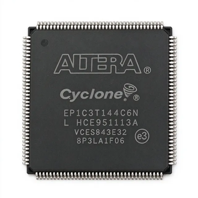
EP1C6T144C6N - Cyclone FPGA 5,980 LEs 144-TQFP | Intel
EP1C6T144C6N

EP1C6T144C6N - Cyclone FPGA 5,980 LEs 144-TQFP | Intel

The Intel (formerly Altera) EP1C6T144C6N is a low-cost Cyclone FPGA from the Cyclone family, delivering 5,980 logic elements, 92,160 bits of embedded RAM, and 98 user I/O pins in a 144-pin TQFP (T144) package with a -6 speed grade and commercial 0C to 85C operating range. The device integrates a 1.5V core, two PLLs, and a 405.2 MHz maximum internal operating frequency, targeting cost-sensitive high-volume applications. A Field Programmable Gate Array (FPGA) is a reconfigurable integrated circuit built from an array of programmable logic blocks, interconnect, and I/O cells that can implement custom digital logic after PCB assembly. FPGAs sit in the programmable logic device hierarchy between fixed-function ASICs and CPLDs, combining the high integration of ASICs with the flexibility of post-fabrication reconfiguration. The Cyclone family specifically occupies the low-power, low-cost node of Intel's FPGA portfolio, optimized for glue logic, parallel processing, and interface bridging. Key features of the EP1C6T144C6N include 5,980 logic elements, 92,160 RAM bits distributed in M4K blocks, two PLLs for clock management, 98 maximum user I/O pins arranged as eight I/O banks, and support for LVTTL, LVCMOS, PCI, SSTL-2, and SSTL-3 I/O standards. The 1.5V core and 144-pin TQFP (22 mm x 22 mm body, 0.5 mm pitch) footprint keep board-level integration simple for legacy through-hole-style PCB manufacturing flows. The device is fabricated on a 0.13-micron SRAM-based process, which makes the configuration volatile and requires an external configuration device (typically an EPCS1 or EPCS4 serial flash) to load the bitstream at power-up. The Cyclone architecture combines 4-input look-up tables (LUTs), embedded memory, and DSP-friendly multiplier blocks, making the EP1C6 well suited to digital signal processing, custom bus interfaces, and industrial control applications where deterministic parallel logic outperforms microcontrollers. Typical applications include industrial automation controllers, video processing and image aggregation, consumer electronics glue logic, communications protocol bridging (UART, SPI, I2C, Ethernet MAC front-ends), and legacy ASIC replacement. The Cyclone EP1C6 is widely used in 32-bit RISC soft-core implementations (Nios II) and in parallel sensor aggregation hubs for camera and machine-vision front ends. When designing with the EP1C6T144C6N, allocate a configuration flash device (EPCS1/EPCS4) on the JTAG-friendly 4-wire serial bus (nCONFIG, nSTATUS, CONF_DONE, DCLK) and reserve at least four pins for the JTAG chain. Decouple VCCINT (1.5V) and VCCIO (1.5V/1.8V/2.5V/3.3V) rails with bulk plus high-frequency ceramic capacitors placed as close to the pins as the TQFP allows. This page synthesizes distributor pricing, pin-compatible drop-in alternatives on the same 144-TQFP footprint, and practical design notes not found in the manufacturer datasheet alone.

견적 요청 문의하기
EP1C6T144C7 - Cyclone FPGA 5980 Logic Elements 144-LQFP
EP1C6T144C7

EP1C6T144C7 - Cyclone FPGA 5980 Logic Elements 144-LQFP

The Altera (Intel) EP1C6T144C7 is a Cyclone family Field-Programmable Gate Array (FPGA) integrating 5,980 logic elements, 92,160 RAM bits, and 98 user I/O pins in a 144-pin TQFP/LQFP package. It is fabricated on a 130 nm process, operates from a 1.5 V core supply with 3.3 V I/O tolerance, and supports up to 320 MHz internal operation. The device belongs to the original Cyclone generation that introduced a low-cost FPGA architecture for high-volume applications. A Field-Programmable Gate Array (FPGA) is a programmable logic device containing an array of configurable logic blocks (CLBs) interconnected via a programmable routing fabric. The Cyclone family sits within Altera's mid-density product hierarchy, between the smaller Cyclone II entry parts and the higher-end Stratix devices. FPGAs enable designers to implement custom digital logic, glue logic, and parallel processing functions that can be reconfigured after PCB assembly, making them distinct from fixed-function ASICs and from CPLDs that target simpler glue-logic tasks. Key features include 5,980 logic elements distributed across 598 logic array blocks (LABs), 92,160 bits of embedded RAM, two phase-locked loops (PLLs) for clock management, and 98 user I/O pins supporting LVTTL, LVCMOS, SSTL, and differential I/O standards. The device integrates dedicated 18 x 18 hardware multipliers that support DSP functions such as FIR filters and video processing without consuming general-purpose logic. The Cyclone architecture combines a four-input look-up-table logic element with embedded memory blocks, multiplier blocks, and PLL clock networks. The 130 nm process node balances cost and performance, with the TQFP-144 package providing a low-cost plastic platform suitable for prototype and moderate-volume production where BGA packages would be uneconomical. Typical applications include industrial control, video processing, consumer electronics, communications glue logic, and educational prototyping boards. The combination of moderate logic capacity, embedded multipliers, and a low-cost TQFP package makes the EP1C6T144C7 particularly suitable for designs transitioning from discrete logic or CPLD-based implementations. When designing with this device, ensure the Quartus II design software is used (legacy versions support the original Cyclone family), and verify that the 1.5 V core supply is well-decoupled with bulk and high-frequency ceramic capacitors placed close to the VCCINT pins. This page synthesizes distributor pricing, same-family drop-in alternatives, and design notes that complement the original Altera datasheet for engineers maintaining legacy Cyclone I designs.

견적 요청 문의하기
EP1C6T144C7N - Cyclone 5980-Cell FPGA, 1.5V, 144-TQFP | Altera
EP1C6T144C7N

EP1C6T144C7N - Cyclone 5980-Cell FPGA, 1.5V, 144-TQFP | Altera

The Altera (Intel) EP1C6T144C7N is a Cyclone-series Field Programmable Gate Array (FPGA) with 5980 logic cells, 92160 bits of embedded SRAM, and 98 user I/Os, housed in a 144-pin TQFP (Thin Quad Flat Pack) package measuring 22x22 mm with 0.5 mm pitch. The device is fabricated on a 1.5V CMOS process and operates at a maximum internal frequency of approximately 320 MHz, making it well suited for cost-sensitive digital logic, glue logic, and parallel processing applications. A Field Programmable Gate Array (FPGA) is a semiconductor device built around an array of configurable logic blocks (CLBs), programmable interconnect, and I/O cells. Unlike an ASIC, an FPGA's function is defined by a user-supplied bitstream loaded into on-chip SRAM configuration memory. The Cyclone family occupies the low-cost, high-volume segment of the FPGA hierarchy (FPGA -> programmable logic -> programmable logic device -> semiconductor) and is commonly used as a bridge between discrete logic and higher-density FPGAs such as Stratix. Key features of the EP1C6T144C7N include 5980 logic elements, 5980 CLBs (equivalent to 1 logic array block per 10 LEs), 20 M4K RAM blocks providing 92160 bits of embedded memory, two PLLs for clock management, and LVTTL/LVCMOS/PCI I/O support with hot-socketing capability. The device supports configuration via passive serial (PS), active serial (AS), and JTAG modes, and offers low-power operation compared to earlier SRAM FPGAs. The TQFP-144 package is lead-free and RoHS compliant. Architecturally, the EP1C6T144C7N is built on a 130 nm SRAM-based CMOS process with a Look-Up Table (LUT)-based logic fabric and a hierarchical interconnect routing architecture. Each Logic Element (LE) contains a 4-input LUT, a programmable register, and carry chain logic for arithmetic functions. The M4K memory blocks can be configured as RAM, ROM, or FIFO and support true dual-port operation, enabling efficient data buffering in DSP and communications pipelines. Typical applications include digital signal processing front-ends, industrial control and motor control logic, telecommunications interface bridges, video processing pipelines, prototype ASIC emulation, and embedded coprocessors in microcontroller-plus-FPGA designs. The combination of moderate logic density, abundant I/O, and low unit cost also makes it attractive for educational platforms and low-volume production. When designing with the EP1C6T144C7N, ensure clean 1.5V core and 3.3V I/O power rail decoupling, with multiple bulk and high-frequency ceramic capacitors placed close to the package pins. Use the Altera Quartus II design suite for synthesis, place-and-route, and bitstream generation. Verify JTAG chain integrity before attempting configuration and observe the device's configuration setup and hold timing for the chosen mode. This page synthesizes verified distributor pricing, same-package drop-in alternatives from the Cyclone I family, and practical design notes not consolidated in the manufacturer datasheet.

견적 요청 문의하기
EP1C6T144C8 - Cyclone FPGA 5980 LE, 98 I/O | Altera
EP1C6T144C8

EP1C6T144C8 - Cyclone FPGA 5980 LE, 98 I/O | Altera

The Altera EP1C6T144C8 is a Cyclone family field-programmable gate array integrating 5,980 logic elements, 92,160 RAM bits, and 98 user I/Os in a 144-pin TQFP (commonly listed as 144-LQFP) package. It operates from a 1.5 V core supply and is built on a 0.13 μm all-layer copper SRAM process, targeting low-cost, high-volume applications with commercial temperature-grade ordering options. A field-programmable gate array is an integrated circuit whose logic fabric can be configured after manufacturing. Unlike fixed-function ASICs, it contains programmable logic elements, embedded memory, and I/O blocks whose interconnects are set by SRAM configuration bits. In the device hierarchy, an FPGA is a programmable logic device within the broader category of integrated circuits; it offers hardware-like parallelism with software-like reconfigurability. Cyclone devices belong to Altera's low-cost FPGA family, positioned for applications that need dense parallel logic but do not require high-end transceivers or hardened processors. The EP1C6T144C8 provides 5,980 logic elements, 92,160 bits of on-chip RAM, and 98 user I/O pins, making it suitable for glue logic, bus interfaces, and modest state machines. The 1.5 V core and 130 nm copper SRAM process deliver lower dynamic power than older 2.5 V FPGAs. The 144-pin TQFP package is a conventional surface-mount form factor with exposed leads that ease inspection and rework compared to fine-pitch BGA packages. The device supports JTAG boundary-scan testing and in-system configuration. Internally, Cyclone FPGAs consist of logic array blocks containing multiple logic elements, embedded memory blocks, and clock management resources; however, exact M4K block and PLL counts for EP1C6 were not enumerated in the retrieved data and should be confirmed in the Cyclone FPGA Family Data Sheet. The architecture is SRAM-based, so configuration data is volatile and must be loaded from an external configuration device or host at every power-up. The I/O ring supports multiple single-ended interface standards, and the JTAG interface is used for both boundary-scan and configuration. Typical applications include motor-control interface logic, display and sensor bridging, protocol conversion between UART/SPI/I2C and parallel buses, test equipment sequencing, and low-cost prototyping for students and hardware engineers. The large I/O count and 5,980 LEs are enough for state machines and data-path glue, while the TQFP package allows two-layer PCBs in many designs. When designing with this device, verify the configuration scheme early. Because Cyclone FPGAs have no internal flash, they require an EPCS serial configuration device or a configuration host holding the SRAM bitstream; the selected scheme affects board area and BOM cost. This data page synthesizes distributor availability, lead-free and speed-grade drop-in alternatives, package comparison data, and practical design guidance not stated in the bare datasheet extract, giving engineers a single-source decision reference for the legacy Cyclone family.

견적 요청 문의하기
EP1C6T144C8 - Cyclone FPGA, 5980 LEs, 98 I/O, 144-TQFP | Intel
EP1C6T144C8

EP1C6T144C8 - Cyclone FPGA, 5980 LEs, 98 I/O, 144-TQFP | Intel

The Intel (Altera) EP1C6T144C8 is a Cyclone® family Field Programmable Gate Array (FPGA) fabricated on a 130 nm process, offering 5980 logic elements in a 144-pin TQFP surface-mount package. The device integrates 92160 bits of embedded RAM and provides 98 user I/O pins, with a core voltage of 1.5 V and supporting I/O standards from 1.5 V to 3.3 V. The "C8" suffix denotes the commercial temperature grade (0 °C to +70 °C) and the -8 speed grade. An FPGA (Field Programmable Gate Array) is a type of programmable logic device that allows designers to configure digital logic circuits after manufacture. FPGAs occupy a unique position in the semiconductor hierarchy: more flexible than Application-Specific Integrated Circuits (ASICs) and far more capable than discrete logic ICs. Within the programmable logic taxonomy, the Cyclone family belongs to the low-cost, high-volume segment, sitting below the more advanced Stratix and above the legacy MAX CPLD families. Cyclone devices use a LUT-based logic element fabric with embedded M4K RAM blocks and a network of programmable interconnect. Key features of this Cyclone part include 5980 logic elements distributed across LABs (Logic Array Blocks), two PLLs for clock management, 20 embedded multipliers (18x18-bit) for DSP-style operations, and 5980 equivalent LEs supporting 100 MHz internal operation. The 130 nm process delivers a fine balance of cost, power, and performance for cost-sensitive applications. The 144-pin TQFP package provides a low-cost, easy-to-inspect footprint suitable for prototype, low-volume, and educational designs, with the trade-off of limited pin density compared with BGA alternatives. Typical applications include digital signal processing, glue logic, custom state machines, video and image processing front ends, industrial control, and educational/development platforms. The Cyclone architecture is supported by the Intel Quartus® II (now Intel Quartus Prime) design software, which includes ready-made IP cores for common functions such as UART, I2C, SPI, DDR controllers, and Nios II embedded processors. When designing with EP1C6T144C8, ensure the Quartus II pin assignments match the device pin-out for the 144-pin TQFP package and that decoupling capacitors are placed as close as possible to each VCCINT and VCCIO pin. The configuration scheme (AS, AP, PS, JTAG) must be selected before board layout to allocate correct pins for configuration. This page synthesizes distributor pricing, drop-in Cyclone alternatives, and practical Quartus design notes not aggregated in the original datasheet.

견적 요청 문의하기
EP1C6T144C8AA - Cyclone FPGA, 6K LEs, 144-LQFP | Intel
EP1C6T144C8AA

EP1C6T144C8AA - Cyclone FPGA, 6K LEs, 144-LQFP | Intel

The Intel EP1C6T144C8AA is a member of the original Cyclone FPGA family, delivering 5,980 logic elements and 92,160 bits of embedded RAM in a 144-pin LQFP package with 98 user I/O pins. Speed grade 8 is the slowest commercial-tier speed bin, while the trailing "AA" suffix designates a lead-free, industrial-temperature-grade offering. According to the Cyclone Family datasheet, the device is built on a 1.5 V core, 0.13 µm SRAM-based process with an internal PLL block (up to two PLLs) and dedicated LVDS support, making it a low-cost programmable fabric for glue logic, bus bridging, and parallel DSP preprocessing. A field programmable gate array (FPGA) is a semiconductor device built around an array of configurable logic blocks (CLBs), programmable interconnect, and I/O cells, all of which are defined by a user-supplied bitstream held in external SRAM or flash. FPGAs sit between fixed-function ASICs and software-driven microcontrollers in the digital design hierarchy: they deliver ASIC-class parallelism and I/O flexibility without NRE cost, while offering far more deterministic real-time performance than general-purpose CPUs. The Cyclone family was Intel's (formerly Altera's) first low-cost FPGA line and helped define the modern mid-density FPGA market segment. Key features of the EP1C6T144C8AA include 5,980 logic elements, 92,160 RAM bits (approximately 11.5 Kbytes of block RAM), up to 185 Kbits of usable RAM, two PLLs, and support for LVDS, LVTTL, LVCMOS, SSTL, and PCI I/O standards. The 144-LQFP package exposes 98 user I/Os across four I/O banks, supporting up to 4 user I/O banks per Cyclone device. Industrial temperature range is -40 °C to +100 °C junction, making the part suitable for harsh environments. The device is configured via active serial (AS), passive serial (PS), or JTAG modes using an external configuration device. Architecturally, the EP1C6T144C8AA uses a four-input look-up-table (LUT) per logic element, M4K RAM blocks of 4 Kbits each (with parity and shift-register modes), and dedicated multiplier blocks are not present in this family (multipliers are implemented in soft logic using the Quartus Prime library megafunctions). The two PLLs support clock multiplication, division, phase shifting, and external clock output, enabling robust clock-tree design across the 98 I/Os. Typical applications include industrial motor control and factory automation glue logic, video processing and image-sensor interface bridging, low-cost ASIC prototyping, communications backplane interfacing, and consumer display controllers. Designers migrating from discrete logic or CPLDs frequently choose this device for its RAM density and PLL support. When designing with this part, ensure the JTAG chain, configuration flash, and decoupling network are correctly designed. Quartus II (or the legacy Quartus Prime 13.0sp1) is the supported development toolchain; third-party synthesis from Synopsys Synplify or Mentor Precision is also available. This page synthesizes verified distributor pricing, drop-in alternatives, and practical design notes not consolidated on a single manufacturer or distributor page.

견적 요청 문의하기
EP1C6T144C8N - Cyclone FPGA 5980 LE 144-TQFP | Intel / Altera
EP1C6T144C8N

EP1C6T144C8N - Cyclone FPGA 5980 LE 144-TQFP | Intel / Altera

The Intel (formerly Altera) EP1C6T144C8N is a low-cost Cyclone® Field Programmable Gate Array (FPGA) delivering 5,980 logic elements, 92,160 bits of embedded RAM, and 98 user I/O pins in a 144-pin TQFP package with a commercial 0°C to +85°C operating range. The device is built on a 1.5 V, 0.13 µm all-layer copper SRAM process and is offered in the -C8 speed grade targeting up to 275 MHz internal operation, making it a long-standing workhorse for cost-sensitive digital designs, glue logic, and legacy industrial platforms. An FPGA (Field Programmable Gate Array) is a reprogrammable semiconductor that lets engineers implement arbitrary digital logic - from simple state machines to soft processor cores - by configuring an on-chip array of look-up tables, flip-flops, and programmable interconnect. FPGAs sit in the broader taxonomy of programmable logic devices (PLD), above simple CPLDs in capacity and below ASICs in per-unit cost but with the crucial advantage of in-system reprogrammability. The Cyclone family specifically targeted low power and low cost per logic element, opening FPGAs to volume consumer and industrial markets previously served only by ASICs or microcontroller-based designs. Key features of the EP1C6T144C8N include two PLLs for clock multiplication and phase shifting, dedicated 18x18 multipliers for DSP-style arithmetic, support for external memory interfaces including DDR SDRAM and FCRAM, and an active serial (AS) configuration interface compatible with low-cost EPCS configuration devices. The 144-TQFP package provides 98 usable I/O pins arranged in four I/O banks, allowing flexible mixed-voltage interfacing through bank-level VCCIO rails. Typical applications include industrial control and factory automation backplanes, motor control and inverter drive boards, telecommunications line cards and protocol bridges, low-cost video processing pipelines, education and development kits, and replacement of legacy glue-logic ASICs where the original mask set is unavailable. Long product-life status and broad Quartus II tool support have made it a default choice for sustaining engineering. When designing with the EP1C6T144C8N, engineers should plan for a 1.5 V core supply with separate VCCIO bank rails and observe the I/O bank voltage grouping rules documented in the Cyclone device handbook. Configuration memory must be loaded at every power-up from a non-volatile EPCS device or a JTAG/USB-Blaster programmer; the device does not retain configuration when powered down. Thermal management is straightforward thanks to the plastic TQFP package and modest static plus dynamic power dissipation. This page synthesizes Cyclone family datasheet parameters, distributor stock and pricing snapshots, and drop-in same-footprint alternatives (C6/C7 speed grades, I-grade temperature variants, and 144-TQFP Cyclone I siblings) to help engineers compare, source, and sustain EP1C6T144C8N-based designs.

견적 요청 문의하기
EP1C6T144I-7 - Cyclone FPGA, 5980 LEs, 144-LQFP | Altera
EP1C6T144I-7

EP1C6T144I-7 - Cyclone FPGA, 5980 LEs, 144-LQFP | Altera

The Altera (now Intel) EP1C6T144I-7 is a member of the Cyclone family of low-cost Field Programmable Gate Arrays (FPGAs) fabricated on a 130 nm process. It integrates 5,980 logic elements, 92,160 bits of embedded RAM organized in M4K blocks, and two PLLs into a 144-pin LQFP package (TQFP, 0.5 mm pitch). The device is rated for an industrial operating temperature range of -40 °C to +100 °C and supports a core supply voltage of 1.5 V with I/O banks tolerant of common logic standards. A Field-Programmable Gate Array (FPGA) is a semiconductor device built around an array of configurable logic blocks (CLBs) connected via programmable interconnect, allowing designers to implement arbitrary digital logic, glue logic, DSP pipelines, and parallel processing engines after PCB assembly. Within the power-management and embedded-system hierarchy, the Cyclone family belongs to the low-cost SRAM-based FPGA category, positioned below high-performance Stratix devices and above CPLDs in terms of density and DSP capability. The 130 nm CMOS process and 1.5 V core make EP1C6T144I-7 a mature, low-power entry point. Key features of the EP1C6T144I-7 include 5,980 logic elements, 92,160 embedded RAM bits (twenty M4K blocks of 4,608 bits each), a maximum internal clock frequency up to 320 MHz (speed grade -7), two general-purpose PLLs with four output taps each, and 98 maximum user I/O pins. The device also integrates a JTAG boundary-scan interface, supports configuration via passive serial, active serial, or JTAG modes, and is supported by the Quartus II / Quartus Prime design toolchain. The '-7' speed grade denotes one of the faster Cyclone tiers. Architecturally, the Cyclone device pairs four-input look-up tables (LUTs) with small embedded memory blocks, enabling efficient shift-register, FIFO, and DSP-style FIR filtering implementations without external memory. The two PLLs provide on-chip clock multiplication and phase shifting, eliminating many external clock-generator ICs. Combined with the LVDS, LVTTL, SSTL, and PCI I/O standards supported, EP1C6T144I-7 is engineered for high-volume cost-sensitive applications that require integration density beyond discrete CPLDs. Typical applications include industrial control and instrumentation, motor-control front-ends, consumer-electronics glue logic, embedded video processing for legacy CCTV and digital signage, telecommunications line-card glue logic, and educational / FPGA-training platforms. The 144-pin LQFP package allows hand-soldering and rework on 2-layer prototype boards, which is a key reason this part persists in low-volume production despite newer Cyclone generations. When designing with EP1C6T144I-7, note that the part contains lead (Pb) and is not RoHS compliant - for RoHS designs, use EP1C6T144I7N or newer Cyclone devices. The 1.5 V core requires a dedicated LDO regulator, and all four PLL analog supply pins (VCCA_PLL) must be decoupled with 0.1 µF and 10 µF capacitors per the datasheet typical application circuit. This page synthesizes distributor pricing, drop-in same-brand alternatives from the Cyclone family, and practical design notes not found in the bare manufacturer datasheet.

견적 요청 문의하기
EP1C6T144I6ES - Cyclone FPGA, 5,980 LEs, TQFP-144 | Intel (Altera)
EP1C6T144I6ES

EP1C6T144I6ES - Cyclone FPGA, 5,980 LEs, TQFP-144 | Intel (Altera)

The Intel (formerly Altera) Cyclone EP1C6T144I6ES is a low-cost, low-power field-programmable gate array (FPGA) from the original Cyclone family, providing 5,980 logic elements (approximately 1,980 logic array blocks / 5980 CLBs per the legacy marketing spec) in a 144-pin TQFP package with 0.5 mm pitch. The device operates over the industrial temperature range (-40C to +100C) and is qualified to the I6 industrial speed grade, supporting an internal clock performance envelope of approximately 405 MHz depending on logic utilization. An FPGA (Field-Programmable Gate Array) is a semiconductor device built around an array of configurable logic blocks (CLBs/LABs), programmable interconnect, and embedded memory blocks that the user can re-program after manufacture to implement arbitrary digital logic. FPGAs sit at the top of the programmable logic hierarchy alongside CPLDs and ASICs, and offer the best balance of density, performance, and time-to-market for mid-complexity glue logic, bus interfacing, and signal-processing pipelines. The Cyclone family is positioned at the entry/low-power tier of the Altera (now Intel PSG) portfolio, above CPLDs and below the Cyclone II/III/IV/V and Stratix families. Key features of the EP1C6T144I6ES include 5,980 LEs, approximately 92 Kbits of embedded RAM distributed across M4K blocks, two PLLs per device for clock multiplication and phase shifting, and support for LVDS, LVTTL, LVCMOS, SSTL-2, and SSTL-3 I/O standards through the 144-pin TQFP exposed-pad package. The TQFP-144 footprint is a 22 mm x 22 mm body with 0.5 mm pitch and gull-wing leads, fully lead-free and RoHS-compliant, with a maximum seated height of 1.6 mm. Architecture-wise, the EP1C6 implements a 1.5 V core voltage with a 4-wire passive serial or JTAG configuration interface, supports configuration via Altera EPC configuration devices, and is fabricated on a 0.13 um SRAM process node. Logic is built from 4-input look-up tables (LUT4) grouped into Logic Array Blocks (LABs), each LAB containing ten LEs. Embedded multiplier support is not present in this generation (multipliers were introduced in Cyclone II), so DSP functions are typically implemented as soft logic. Typical applications of the EP1C6T144I6ES include industrial control boards, glue-logic bridging between microprocessors and peripherals, video/display interface conversion (e.g., ITU-R BT.656 capture), serial-protocol bridging (UART/SPI/I2C expansion), low-volume prototyping for ASIC replacement, and educational platforms where a through-hole-friendly 0.5 mm-pitch TQFP simplifies manual rework. Designers should note that the EP1C6 family supports vertical migration within the same TQFP-144 footprint across the EP1C3 and EP1C6 density points, enabling a single PCB layout to serve multiple logic-capacity SKUs. The 'I6' suffix denotes the industrial temperature range and the slowest speed grade in the family; faster 'I7' and 'I8' variants are available for timing-critical designs. This page synthesizes verified distributor pricing, same-package drop-in alternatives, and practical Quartus II / Quartus Prime legacy toolchain notes not consolidated in the manufacturer datasheet alone.

견적 요청 문의하기
EP1C6T144I6N - Cyclone FPGA 5980 Cells 144-TQFP | Altera / Intel
EP1C6T144I6N

EP1C6T144I6N - Cyclone FPGA 5980 Cells 144-TQFP | Altera / Intel

The Altera (now Intel Programmable Solutions Group) EP1C6T144I6N is a member of the first-generation Cyclone FPGA family, delivering 5,980 logic elements in a 144-pin Thin Quad Flat Pack (TQFP) package. It is fabricated on a 1.5V, 130 nm CMOS process, operates at an internal core clock up to 405.2 MHz, and is targeted at cost-sensitive, high-volume digital logic designs that previously used discrete gate arrays or CPLDs. The 'I6' speed/temperature grade indicates an industrial temperature range (-40 C to +100 C) with a -6 speed bin, while the 'N' suffix indicates a lead-free, RoHS-compliant assembly. A field-programmable gate array (FPGA) is a semiconductor integrated circuit that can be configured by the customer after manufacture to implement arbitrary digital logic. The Cyclone family sits in the taxonomy: FPGA -> programmable logic device (PLD) -> digital logic IC -> semiconductor. FPGAs bridge the gap between fixed-function ASICs (low unit cost, no flexibility) and microcontrollers (flexible, but limited performance for parallel workloads). Cyclone devices contain an array of configurable logic blocks (LABs), embedded memory (M4K blocks), phase-locked loops (PLLs), and programmable I/O, all interconnected by a programmable routing fabric. Key features of the EP1C6T144I6N include approximately 5,980 logic elements, around 90 Kbits of embedded RAM (M4K blocks), two PLLs for clock multiplication and phase shifting, and 100+ user I/O pins. The device supports a wide range of I/O standards including LVTTL, LVCMOS, PCI, SSTL, and LVDS, making it interoperable with common microprocessors, memories, and bus interfaces. Configuration is typically loaded from an external EPC serial configuration device or via JTAG, enabling in-system reprogrammability for field upgrades. The Cyclone architecture uses a 1.5V core with separate VCCIO banks that can be powered at 1.5V, 1.8V, 2.5V, or 3.3V to interface with mixed-voltage peripherals. Its built-in multipliers and dedicated routing make it well suited to DSP-style data paths, while the abundant M4K blocks provide efficient on-chip buffering for FIFOs, lookup tables, and small frame stores. Typical applications include industrial control and machine vision glue logic, motor control co-processors, low-cost software-defined radio front-end controllers, communication bridges (UART/SPI/I2C aggregation), LED video wall scan-and-refresh drivers, and education/hobby digital design platforms. The 144-TQFP package has generous pitch (0.5 mm) that is friendly to hand-soldering and four-layer prototype boards. When designing with this part, plan for a stable 1.5V core supply, a separate VCCIO rail per bank, and a configuration mode (AS, PS, JTAG). Decouple every VCC/VCCIO pin with 0.1 uF and 10 uF bulk capacitors placed as close to the package as possible. The Cyclone handbook (Altera Cyclone Device Handbook) provides reference schematics and Quartus II pinout files for the 144-pin TQFP. This page synthesizes distributor availability, drop-in same-package alternatives within the Cyclone family, and practical design notes not found in the manufacturer datasheet, helping engineers quickly evaluate the EP1C6T144I6N for both new designs and legacy board re-spins.

견적 요청 문의하기
EP1C6T144I7 - Cyclone FPGA, 5980 LE, 144-LQFP | Intel / Altera
EP1C6T144I7

EP1C6T144I7 - Cyclone FPGA, 5980 LE, 144-LQFP | Intel / Altera

The Intel (formerly Altera) EP1C6T144I7 is a Cyclone-series Field Programmable Gate Array (FPGA) built on a 1.5V core, 130nm process technology, offering 5,980 logic elements, 92,160 RAM bits, and 98 user I/Os in a 144-pin LQFP (TQFP) package. It operates across the industrial temperature range of -40C to +100C and supports configuration via JTAG, Active Serial, or Passive Serial modes, making it a drop-in upgrade for designers leaving the legacy Cyclone I family. A Field Programmable Gate Array (FPGA) is a type of programmable logic device (PLD) belonging to the integrated circuit family that allows hardware designers to configure digital logic blocks, routing, and I/O after fabrication. Within the broader taxonomy, the EP1C6T144I7 sits as: FPGA -> programmable logic device -> logic IC -> integrated circuit -> semiconductor. FPGAs are commonly used to implement glue logic, custom state machines, bus bridges, DSP datapaths, and parallel I/O expansion where ASIC NRE costs are not justifiable. Key features include 5,980 logic elements distributed across 598 LABs (logic array blocks), 92,160 bits of embedded SRAM organized as M4K blocks, two PLLs for clock management, and 98 user I/O pins supporting LVTTL, LVCMOS, SSTL-2, and SSTL-3 I/O standards. The 144-LQFP package is a plastic thin quad flat pack with 0.5mm pitch and a 22x22mm body, well-suited for low-cost PCB assembly and breadboard-friendly prototyping. Unlike BGA packages, the LQFP allows hand-soldering and standard rework, which keeps NPI costs down. The Cyclone I architecture uses a 4-input look-up table (LUT) per logic element with dedicated carry chains for fast arithmetic and routing resources tuned for high logic density at low power. Its quiescent core voltage of 1.5V (VCCINT) keeps dynamic power modest versus later 90nm/65nm families, while I/O banks tolerate up to 3.3V for mixed-voltage interfacing. The device supports up to 250 MHz internal operation in speed grade -7. Common applications include industrial motor control, factory automation bridges, legacy telecom interface cards, low-cost video processing pipelines, and educational FPGA development platforms. Engineers often select this Cyclone part when migrating off EOL (end-of-life) discrete logic or when budget constraints rule out Cyclone II/III/IV successors. A primary design consideration is supply decoupling: place 0.1uF and 10uF capacitors close to every VCCINT and VCCIO pin, and ensure the JTAG chain includes proper TCK pull-down per IEEE 1149.1. Migration to newer families (Cyclone IV, Cyclone 10) requires footprint change because pin counts and ball maps differ; the EP1C6T144I7 is best retained where its footprint is already in volume production. This page consolidates distributor pricing, verified same-package drop-in alternatives, and design notes not found in the standalone datasheet, giving engineers a single reference for sourcing and selection decisions.

견적 요청 문의하기
EP1C6T144I7N - Cyclone FPGA, 5,980 LEs, 144-LQFP | Intel
EP1C6T144I7N

EP1C6T144I7N - Cyclone FPGA, 5,980 LEs, 144-LQFP | Intel

The Intel (formerly Altera) EP1C6T144I7N is a low-power Cyclone FPGA from the first-generation Cyclone family, delivering 5,980 logic elements, 92,160 RAM bits, and 98 user I/Os in a 144-pin LQFP (TQFP-144) package. It is built on a 0.13 μm SRAM process and operates with a core voltage of 1.5 V plus I/O voltage of 1.5 V to 3.3 V, supporting up to 64 LVDS pairs and 2 PLLs for clock management. The device is targeted at cost-sensitive, high-volume designs that need programmable logic without the cost of an ASIC. What is an FPGA? An FPGA (Field Programmable Gate Array) is a semiconductor IC whose logic fabric, interconnect, and I/O cells can be reconfigured in-circuit to implement arbitrary digital functions. FPGAs sit between fixed-function ASICs and software-driven microcontrollers in the design hierarchy: more flexible than an ASIC, faster and more deterministic than a CPU. The Cyclone family specifically targets consumer, industrial, and communication applications where low unit cost and low static power matter more than raw logic density or transceivers. Key features of the EP1C6T144I7N include 5,980 LEs organized into 598 logic array blocks (LABs), 92,160 bits of embedded M4K RAM (twenty 4-Kbit blocks), 2 PLLs with up to eight output clocks each, and 98 user I/Os arranged across 4 I/O banks supporting LVTTL, LVCMOS, SSTL, and LVDS I/O standards. The device supports configuration via active serial (AS), passive serial (PS), and JTAG modes with EPCS configuration devices. Typical applications include digital signal processing front-ends, video bridging and image processing pipelines, industrial control and machine interfaces, automotive infotainment and body electronics, communication protocol bridging (UART/SPI/I2C to parallel buses), and glue-logic replacement in legacy systems. The wide operating temperature range (-40 °C to +100 °C for the I7 industrial speed grade) and surface-mount TQFP-144 footprint make it suitable for both consumer and industrial PCB designs. When designing with the EP1C6T144I7N, note that the I7 speed grade is the slowest industrial grade available; for designs that close timing marginally, the I8 speed grade (EP1C6T144I8N) provides about 20% higher Fmax at higher cost. This page synthesizes distributor pricing, drop-in alternatives, and practical design notes not found in the manufacturer datasheet alone.

견적 요청 문의하기
EP1C6T144I8 - Cyclone FPGA 5980 LE, 144-TQFP, Industrial | Intel
EP1C6T144I8

EP1C6T144I8 - Cyclone FPGA 5980 LE, 144-TQFP, Industrial | Intel

The Intel (Altera) EP1C6T144I8 is a member of the first-generation Cyclone FPGA family, fabricated on a 1.5V, 130nm CMOS process and delivering 5,980 logic elements, 92,160 RAM bits, and 2 PLLs in a 144-pin TQFP package with industrial temperature grade. What is a Cyclone FPGA? A Field-Programmable Gate Array (FPGA) is a semiconductor device built around an array of configurable logic blocks (CLBs), programmable interconnect, and dedicated hard IP such as block RAM, PLLs, and I/O serializers. Unlike fixed-function ASICs, FPGAs are programmed by the end user after manufacture, making them ideal for prototyping, low-volume production, and designs that must evolve in the field. The Cyclone family sits in the low-cost, low-power tier of the Intel FPGA portfolio - positioned below Cyclone II/III/IV/V and well below Stratix and Arria families. Within this hierarchy: Cyclone -> low-cost FPGA -> programmable logic -> semiconductor IC. The EP1C6 variant occupies the mid-density position in the original Cyclone lineup, between EP1C3 (smaller) and EP1C12/EP1C20 (larger). Key features of the EP1C6T144I8 include 5,980 logic elements, 92,160 bits of embedded RAM (M4K blocks), 98 maximum user I/O pins, two analog PLLs with four outputs each, and support for LVTTL, LVCMOS, SSTL, and differential I/O standards. The 144-TQFP package offers a 1.0mm lead pitch and gull-wing leads compatible with standard SMT assembly and hand-rework, eliminating the need for fine-pitch BGA handling. Technically, the EP1C6T144I8 is built on a 1.5V core with multi-voltage I/O banks supporting 1.5V, 1.8V, 2.5V, 3.3V, and 5.0V interfacing. The device uses SRAM-based configuration memory, requiring a configuration flash or controller on every board. Configuration is via passive serial (PS), active serial (AS), or JTAG. The I8 suffix denotes the industrial temperature grade (-40C to +100C ambient, junction to +135C). Typical applications include industrial motor control, video processing pipelines, custom peripheral expansion, glue logic replacement, software-defined radio front-ends, and educational/development platforms. The Cyclone I/O flexibility makes it well-suited for bridging legacy 5V buses to modern 3.3V processors. When designing with this part, ensure the configuration scheme is selected (AS/PS/JTAG) and that a valid configuration clock source is present at power-up. Unused pins should be left floating per datasheet guidance; the TQFP-144 footprint simplifies prototype bring-up versus BGA alternatives. This page synthesizes distributor pricing, drop-in Cyclone family alternatives, and practical design notes not found in the manufacturer datasheet alone.

견적 요청 문의하기