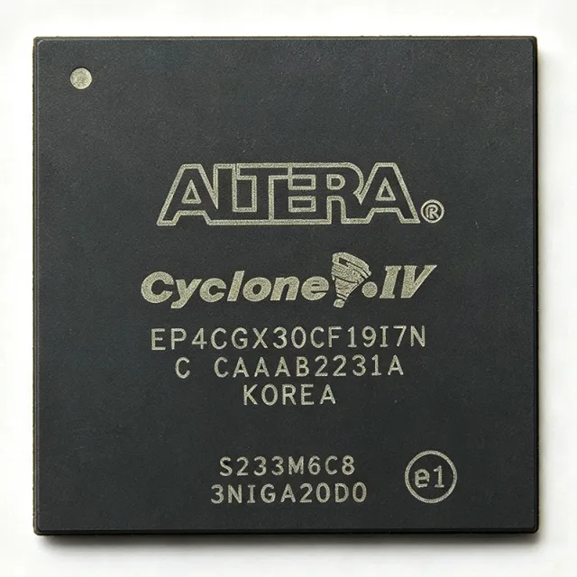
EP4CGX30BF14I7
EP4CGX30BF14I7 - Cyclone IV GX FPGA 29.4K LE | Intel | 169-FBGA
The Intel (Altera) EP4CGX30BF14I7 is a low-power, low-cost Cyclone IV GX field-programmable gate array (FPGA) delivering 29,440 logic elements, 1,105,920 bits of embedded memory, and 72 embedded 18x18 multipliers in a 169-ball FineLine BGA (14x14 mm, 1.0 mm pitch) package. Built on a 60 nm process with a 1.2 V core, the device integrates up to 3.125 Gbps transceivers, dedicated PCIe hard IP, and a wide range of hard memory and DSP blocks, targeting cost-sensitive serial-interface, video, and industrial designs.
An FPGA (Field-Programmable Gate Array) is a reconfigurable integrated circuit containing an array of configurable logic blocks (CLBs), programmable interconnects, and dedicated silicon resources such as block RAM, DSP slices, PLLs, and high-speed transceivers. FPGAs belong to the broader hierarchy of programmable logic devices (PLDs) -> logic ICs -> integrated circuits -> semiconductors, and serve as the prototypical platform for hardware-accelerated DSP, custom parallel I/O, and low-volume ASIC replacement. The Cyclone IV GX family specifically targets applications where low static power, integrated high-speed serial, and an attractive unit cost are all required simultaneously.
Key features of the EP4CGX30BF14I7 include 1840 Configurable Logic Blocks (CLBs), 66 Kbits of distributed RAM, 81 Kbits of M9K block RAM across 66 blocks, four general-purpose PLLs, and up to 290 user I/O pins. The integrated transceiver block supports CPRI, PCIe Gen1 (x1, x2, x4), GigE, SRIO, and Serial Digital Interface (SDI) protocols, eliminating external PHY components on common serial links. The industrial temperature grade (-40C to +100C junction) and Pb-free / RoHS-compliant package suit harsh-environment deployments.
The Cyclone IV GX architecture separates logic, routing, and dedicated blocks into independently optimized tiles. The 18x18 multiplier array supplies 72 DSP elements at up to 250 MHz, sufficient for video processing, baseband datapaths, and motor-control loops. The 1,105,920-bit embedded memory can be configured as true dual-port, simple dual-port, or single-port RAM with parity support, and the configuration scheme supports both passive (JTAG) and active (EPCS) serial flash via the dedicated configuration controller. The I/Os support LVDS, SSTL, LVCMOS, and PCI/PCI-X standards at speeds up to 800 Mbps, with programmable drive strength and slew rate to simplify board-level signal integrity work.
Typical applications include industrial machine vision, broadcast video processing, software-defined radio front-ends, PCIe endpoint cards, and low-cost motor control. The combination of integrated transceivers and PCIe hard IP makes it particularly attractive for embedded computing and factory-automation backplanes.
Designers should pay attention to the multi-rail power architecture (VCCINT, VCCA, VCCIO, VCCPD, VCC_GXB) and the need for a Quartus II / Quartus Prime configuration bitstream. Decoupling and transceiver supply filtering follow the manufacturer reference schematic, which lists recommended ferrite beads, decoupling capacitor counts, and PCB layer-stack assumptions.
This page synthesizes distributor pricing, drop-in compatible package variants, and design notes that complement the manufacturer datasheet and the Quartus device handbook.
견적 요청
문의하기