메모리 IC
하위 카테고리
제품 (875)

PS5012-E12S - PCIe Gen3 x4 NVMe SSD Controller | Phison
The PHISON Electronics PS5012-E12S is a consumer PCIe Gen3 x4 NVMe 1.3 solid-state-drive controller, specified for an operating temperature range of 0°C to 70°C and support for M.2 2280-S2 and M.2 2280-D2 designs. The verified specification identifies a TSMC 28 nm process, a dual-CPU architecture with a built-in 32-bit microcontroller, and support for up to eight NAND channels. A solid-state-drive controller is a semiconductor system that coordinates a host interface, NAND flash channels, DRAM or error-correction resources, firmware, and data-transfer paths. Within the storage hierarchy, the PS5012-E12S is an SSD controller: the completed storage hierarchy is NVMe SSD controller → PCIe interface → NAND storage subsystem → host computer. Its principal role is translating PCIe transactions into NAND operations while providing flash translation, error management, wear leveling, garbage collection, and data integrity functions. The verified material supports PCIe Gen3 x4 operation at 8 GT/s per lane and backward host-interface compatibility with PCIe Gen1 at 2.5 GT/s and Gen2 at 5 GT/s. It complies with the PCI Express Base Specification Revision 3.1 and NVMe 1.3. Reported sequential-read figures in the supplied overview range up to 3400 MB/s, although the exact value depends on the stated SSD capacity and system configuration; Phison cautions that performance may vary with system configuration and test conditions. The E12S platform is associated with consumer capacities from 500 GB through 8000 GB and both TLC and 3D QLC NAND configurations in the supplied specification overview. This makes it relevant to desktop PCs, gaming systems, workstations, and external storage enclosures that expose an M.2 2280 NVMe interface. An SSD implementing the controller still requires qualified NAND, DRAM where applicable, firmware validation, power delivery, thermal management, and electrical compliance testing before it can be treated as a finished drive. Engineering around this controller is not a simple chip-replacement task. The verified sources do not provide a pinout, package dimensions, electrical limits, power consumption, endurance ratings, or qualified board-layout information for PS5012-E12S. Those values must be obtained from the manufacturer’s controlled design package before schematic capture or PCB release. SSD performance should likewise be evaluated at the finished-drive level rather than inferred solely from controller-generation labels. This page consolidates the verified manufacturer specifications, documented interface generations, form-factor context, process technology, and engineering limitations for PS5012-E12S. It also avoids presenting generic BGA variants, functionally similar controllers, or completed SSDs as pin-compatible drop-in replacements because the supplied cross-reference data contains no verified substitute with matching package and pinout.

PS5018-E18 - PCIe 4.0 x4 NVMe Controller | PHISON
The PHISON Electronics Corp. PS5018-E18 is an eight-channel PCIe 4.0 x4 NVMe SSD controller built on a 12 nm FinFET process and housed in a BGA-256 package. It was designed for high-performance consumer solid-state drives using the M.2 2280 form factor. According to the cited SSD hardware reference, the controller uses a dual-core ARM Cortex-R architecture and coordinates PCIe, NAND, flash translation, and error-management functions. The verified product page specifies a commercial operating temperature range of 0°C to 70°C. An NVMe controller is the central semiconductor in a flash-based solid-state drive. It translates a host interface and NVMe command set into operations across multiple NAND channels, manages flash translation, wear leveling, error correction, garbage collection, and data integrity. As an SSD controller, it belongs to the semiconductor hierarchy and coordinates storage media, firmware, DRAM, and the host PCIe interface. Unlike a conventional disk controller, it has no moving parts and must sustain substantially higher random-operation rates. The PS5018-E18's eight-channel architecture is intended for high-throughput solid-state storage, while PCIe 4.0 x4 provides four lanes of host connectivity. The verified data identifies support for PCIe generation and lane configuration but does not provide authoritative controller-level sequential read or write figures. Complete SSDs using this controller have been reported with capacities as high as 8 TB, but capacity and performance belong to the finished drive rather than the controller itself. NAND type, firmware, DRAM, thermal design, and workload also affect measured results. The controller integrates PCIe, NVMe processing, NAND-channel management, and flash-management firmware into one BGA package. It is normally soldered onto an SSD PCB together with NAND packages, DRAM, power-delivery components, and thermal hardware. Because firmware and board design are integral to SSD operation, replacing only the controller in an existing product requires exact electrical, pin, firmware, NAND, and validation support; generic cross-referencing alone does not establish drop-in compatibility. Typical applications include PCIe 4.0 x4 M.2 2280 SSDs, high-end gaming PCs, desktop workstations, notebook storage, and OEM storage platforms. The reported consumer temperature range of 0°C to 70°C suits temperature-controlled consumer environments. An industrial enclosure should not substitute this device without verifying the broader requirements and considering the PS5018-E18DI, whose official listing includes a -40°C to 85°C range. A primary design consideration is total SSD power and heat management. High sequential transfer activity can raise controller and DRAM temperatures, while compact M.2 housings limit airflow. Firmware, NAND compatibility, validation, and thermal throttling must therefore be evaluated as a complete system. The PS5018-E18 is best suited to designers building a new validated SSD platform rather than treating it as a universally interchangeable catalog part.
PS5026-E26 - PCIe 5.0 NVMe SSD Controller | PHISON
The PHISON Electronics PS5026-E26 is a client-grade PCIe 5.0 x4 NVMe SSD controller engineered for high-performance solid-state drives, with sequential throughput up to 14 GB/s. The controller is identified under PCI Vendor ID 1987 and Device ID 5026, and its published operating-temperature range is 0°C to 70°C. The E26 platform is designed for gaming PCs, workstations, content-creation systems, and other client platforms that need a high-throughput storage interface. A PCIe 5.0 NVMe SSD controller is the device inside an SSD that coordinates the host interface, NAND flash, DRAM cache, error correction, and storage-management functions. The PS5026-E26 belongs to the PCIe storage-controller hierarchy: PCIe 5.0 interface, x4 link, NVMe protocol, and client SSD controller. Its 14 GB/s maximum sequential throughput is intended to remove the storage bottleneck in data-intensive workloads such as game loading, large-file transfers, and workstation data preparation. The controller is manufactured using TSMC's 6 nm process according to the SSD Wiki result. Published reference-design information identifies performance configurations up to 14 GB/s read, 12 GB/s write, 1,500K read IOPS, and 2,000K write IOPS. One distributor result lists a configuration rated at 12,000 MB/s read and 10,000 MB/s write, while the manufacturer brochure describes the broader E26 solution reaching up to 14 GB/s. These figures describe the associated SSD platform and should not be treated as guaranteed sequential throughput for every finished drive. The E26 reference designs use an M.2 2280 form factor and a PCIe 5.0 x4 connection. Published material also identifies 232-layer TLC NAND in an engineering-sample 2 TB SSD, demonstrating how the controller can be integrated with external NAND rather than providing a complete SSD by itself. System designers must therefore qualify the NAND, DRAM, firmware, thermal solution, power delivery, and enclosure around the controller. For gaming systems, the controller's high sequential bandwidth can reduce transfer waits when loading large game assets. Workstations benefit when handling large project files, caches, and temporary data. NVMe enclosure and SSD developers can use the E26 as the basis for high-end client drives, provided that thermal dissipation and power management meet the controller's published temperature limits. The main design trade-off is that PCIe 5.0 performance requires careful signal integrity, power delivery, and thermal design. A finished SSD must maintain the specified operating range while sustaining the advertised workload, rather than relying only on short benchmark bursts. This page combines verified manufacturer information, reference-design data, technical entity context, and application guidance for PS5026-E26 evaluation.
PS5029-E29T - PCIe 4.0 x4 DRAMless NVMe Controller
PHISON Electronics Corp. PS5029-E29T is a DRAMless NAND flash controller IC supporting PCIe Gen4 x4 storage interfaces, NAND Flash I/O rates up to 3600 MT/s, and performance up to 7400 MB/s. The controller uses LDPC error-correcting technology to improve NAND compatibility and SSD reliability, while its power- and cost-efficient design targets client solid-state drives. A NAND flash controller is the semiconductor system that coordinates NAND storage media, the host interface, error correction, wear management, and flash translation layers. The PS5029-E29T belongs to the PCIe storage-controller hierarchy and is positioned for modern NVMe SSDs using PCIe Gen4 x4 connectivity. Its DRAMless architecture reduces system complexity and supports efficient SSD designs without an external DRAM cache. The principal verified features are PCIe Gen4 x4 support, NAND Flash I/O up to 3600 MT/s, and performance up to 7400 MB/s. Phison describes the solution as exceeding 7 GB/s bandwidth while maintaining power and cost efficiency. The controller is reported in external database material as a four-channel DRAMless controller in Micron 2600 SSD configurations, while a separate product listing describes an eight-channel configuration; channel count therefore requires confirmation against the specific SSD design source. Typical applications include client NVMe SSDs, M.2 2280 storage products, gaming systems, workstations, and other PCIe Gen4 x4 consumer storage platforms. The PS5029-E29T is especially relevant when an SSD design needs high sequential bandwidth, flexible NAND compatibility, and a DRAMless architecture. Its LDPC implementation is intended to improve error correction as NAND process technology evolves. Designers should validate the exact package, pinout, power rails, NAND-channel organization, firmware requirements, and thermal solution against the current Phison product documentation before layout. SSD performance depends not only on the controller but also on NAND type, firmware, thermal throttling, PCIe topology, and workload. The controller's system-level benefit is strongest when paired with validated NAND and a complete SSD reference design. This page consolidates the verified Phison specifications, application context, source links, and engineering considerations into one technical reference. It distinguishes published controller data from application-level observations so engineers can assess fit without treating third-party SSD configurations as universal specifications.
PS5031-E31T - PCIe 5.0 x4 Gen5 SSD Controller | PHISON
PHISON PS5031-E31T is a DRAMless PCIe Gen5 x4 SSD controller manufactured using TSMC's 7 nm process technology, with a NAND flash I/O rate up to 3600 MT/s and read/write performance up to 10400 MB/s. Designed for high-bandwidth NVMe solid-state drives, it is associated with the M.2 2280 form factor and supports mainstream Gen5 storage applications. An SSD controller is a semiconductor that coordinates the host interface, NAND flash, error correction, data management, and command processing inside a solid-state drive. In the storage hierarchy, the PS5031-E31T is a PCIe Gen5 x4 NVMe controller optimized to move data between a computer and 3D NAND flash without mechanical media. Its DRAMless architecture reduces system complexity while supporting high sequential throughput. Key verified features include a PCIe 5.0 x4 interface, NAND flash I/O up to 3600 MT/s, read/write performance up to 10400 MB/s, a four-channel flash interface with 16 chip-enable signals, and support for capacities up to 8 TB. The controller uses 7th-generation LDPC and RAID ECC with a 4K code word, while its integrated 32-bit microcontroller provides the embedded control function. A 0°C to 70°C operating range suits consumer and mainstream computing environments. The E31T architecture is intended to balance PCIe Gen5 bandwidth, NAND efficiency, and power consumption. Its DRAMless design shifts more storage-management work to controller firmware and on-device resources, which can simplify SSD construction but requires validated flash management. The controller is paired with 3D NAND flash in reference SSD designs; NAND type, firmware, capacity, thermal design, and workload behavior determine the final drive-level performance. Typical applications include M.2 2280 PCIe Gen5 NVMe SSDs for desktop PCs, laptops, workstations, gaming systems, and storage platforms. It can also serve as the core controller in external storage enclosures that expose PCIe Gen5 connectivity. Integration requires a compatible board, power management, thermal design, flash firmware, and validation of PCIe and NAND signal integrity. Designers should verify the exact controller package, pinout, power rails, reference schematic, and firmware-support status with PHISON before layout release. Validate PCIe lane integrity, flash timing, power sequencing, thermal rise, and workload latency using the intended SSD reference design. This page synthesizes verified manufacturer and technical-source data, while distinguishing missing information instead of estimating it.

PSD834F2V-20MI - 2Mb Flash PSD, 3.3V, 200ns, 52-PQFP | STMicroelectronics
The STMicroelectronics PSD834F2V-20MI is a Flash Programmable System Device (PSD) integrating 2 Mbit of primary Flash memory, 256 Kbit of secondary Flash memory, and 64 Kbit of SRAM in a single 52-pin PQFP (10x10 mm) package. Designed for 8-bit microcontroller-based embedded systems, this device operates from a single 3.3V supply (3.0V to 3.6V) and provides 200 ns Flash access time. It combines in-system-programmable (ISP) Flash, a CPLD logic block with optimized macrocell architecture, and a parallel MCU interface, eliminating the need for external memory and glue-logic chips. What is a Flash PSD? A Flash Programmable System Device (PSD) is a single-chip companion memory/logic solution for microcontrollers. It sits hierarchically between an MCU and external memory, integrating Flash, SRAM, and programmable logic. The taxonomy is: PSD -> memory/peripheral companion IC -> embedded system IC -> semiconductor. PSDs are used to expand MCU address space, add boot memory, and consolidate discrete peripheral functions into one footprint. Key differentiating specifications include 2 Mbit primary Flash (256K x 8 organization), 256 Kbit secondary Flash for parameter storage or EEPROM emulation, 64 Kbit SRAM for variable data, an integrated CPLD with macrocell logic for chip-select and decode functions, JTAG-ISP programming support, and parallel interface to 8-bit MCUs such as 8051, 68HC11, and PIC families. The single 3.3V supply simplifies power tree design versus dual-supply memories. Architecturally, the PSD834F2V uses a dual-bank Flash topology - a large main bank for program code and a smaller secondary bank that supports concurrent read while programming. The CPLD section features D-type flip-flops, product-term array logic, and an optimized macrocell that decodes MCU address lines into chip-selects, eliminating the discrete 74HC logic traditionally required around an MCU plus external Flash design. Typical applications include industrial 8-bit MCU expansion, point-of-sale terminals, automotive body controllers, smart meters, UPS front-end controllers, and legacy 8051/PIC system upgrades. When designing, ensure the PSD's interface mode (8-bit multiplexed or separate) matches the MCU bus timing, and observe the 200 ns access time when selecting the MCU oscillator so that no wait-states are required at the target clock.

PSD853F2-90J - 1Mbit Flash ISP PSD, 5V, 90ns, 52-PLCC | STMicroelectronics
The STMicroelectronics PSD853F2-90J is a 5V Flash In-System Programmable (ISP) peripheral for 8-bit microcontrollers, integrating 1 Mbit of primary flash memory, 256 Kbit of secondary flash, SRAM, and programmable logic into a single 52-pin PLCC package. It features dual-bank flash with 8 uniform sectors in the primary array and 4 uniform sectors in the secondary array, plus 90 ns access time for code execution and data retrieval. The device operates from a single 4.5V to 5.5V supply and supports in-system programming via standard microcontroller buses. A Programmable System Device (PSD) belongs to the broader category of memory-plus-logic ICs and sits hierarchically between discrete flash memory and a microcontroller in embedded designs. By consolidating non-volatile storage, volatile memory, and configurable I/O/PLD logic into one package, PSD devices remove the need for external memory chips, latches, and glue logic that historically accompanied 8-bit MCU designs. The PSD853F2 family specifically targets cost-sensitive 8051, 68HC11, and other 8-bit MCU platforms that require field-upgradeable firmware storage without sacrificing board space. Key features of the PSD853F2-90J include its dual-bank flash architecture supporting simultaneous read-while-write operation, an integrated PLD with macro cells for address decoding and chip-select logic, 27 programmable I/O pins, JTAG/ISP programming interfaces, and a 90 ns access time suitable for 8-bit MCU bus speeds. The 52-pin PLCC (J-bend) package provides robust through-hole-style soldering suitable for industrial and commercial environments up to 70 degrees C operating temperature. The internal architecture combines a flash memory controller, SRAM block, dual PLD arrays (DPLD and GPLD), and I/O ports under a unified configuration register space accessed through the MCU bus. The flash memory uses a sector-erase architecture with hardware write protection, while the PLD logic implements sum-of-products expressions evaluated on every bus cycle to generate chip selects and steering logic automatically. Typical applications for the PSD853F2-90J include industrial control panels, point-of-sale terminals, automotive body controllers (non-safety), legacy 8051 firmware expansion modules, and consumer appliance controllers. The integrated PLD enables designers to replace 2-4 discrete logic chips with a single programmable device. When designing, engineers should verify that the MCU bus timing meets the 90 ns access time requirement and that the JTAG/ISP programming header is accessible on the PCB for firmware updates. The PSDsoft Express configuration tool is required to define flash partitioning, PLD equations, and I/O assignments. This page synthesizes distributor stock, parametric alternatives, and design notes that go beyond the manufacturer datasheet, including practical comparisons to similar PSD family devices and recommendations for new designs versus legacy migrations.
PSD854F2-90JI - 2Mbit ISP Flash MCU Peripheral, 5V, 52-PLCC | STMicroelectronics
The STMicroelectronics PSD854F2-90JI is a 5 V Flash In-System Programmable (ISP) peripheral for 8-bit microcontrollers, integrating up to 2 Mbit of primary Flash memory (8 uniform sectors) plus 256 Kbit of secondary Flash memory (4 uniform sectors), 27 programmable I/O pins, and on-chip programmable logic, housed in a 52-pin Plastic Leaded Chip Carrier (PLCC, 19.1 x 19.1 mm) with J-leads. What is an "MCU peripheral" IC? This family of PSD (Programmable System Device) ICs sits alongside an external 8-bit MCU and provides the non-volatile storage, glue logic, and I/O expansion that an MCU alone cannot economically deliver. The PSD854F2-90JI sits in the hierarchy: PSD8xx family -> ISP flash peripheral -> memory IC -> programmable logic -> semiconductor. By combining dual-bank Flash, SRAM, decode PLD, and 27 I/O cells in one package, the part replaces a discrete Flash, latch, PLD, and bus-expander chipset in legacy 8051, 80C31, and similar 8-bit designs. Differentiating features of the PSD854F2-90JI include 90 ns maximum access time, parallel memory-mapped interface, ISP via JTAG/serial, sector-erase granularity for boot-code protection, and a wide 4.5 V to 5.5 V supply range that matches 5 V-tolerant MCU buses. The on-chip decode PLD (DPLD) and general-purpose PLD allow address-latch/decoder functions to be absorbed into the device, freeing the host MCU from software-managed timing. The architecture uses a dual-bank Flash array with independent read-while-write support and a charge-pump-generated 12 V programming voltage on-chip, eliminating an external high-voltage supply. Hardware sector protection prevents bootloader tampering, and the 27 I/O cells can be configured as standard CMOS, slew-rate-limited, or Schmitt inputs to match industrial buses. Typical applications include 8-bit industrial controller firmware storage, ISA-bus retrofit cards, point-of-sale terminals, automotive body-control modules (pre-CAN era), vending-machine controllers, and legacy 8051 firmware expansion. The 90 ns access time aligns with the bus timing of classical 8051, 80C186, and similar MCUs running at up to ~12 MHz without wait states. When designing with this part, dedicate one secondary Flash sector to the boot loader and lock its protect bits before end-of-line; this prevents field reprogramming from overwriting the rescue image. Decouple VCC with a 0.1 uF ceramic plus 10 uF tantalum as close as possible to pins 1, 12, 24, and 35, and route the JTAG signals away from switching regulators to preserve ISP margin. This page synthesizes real distributor pricing, verified cross-references for the legacy PSD8xx family, and PCB-level design guidance not consolidated in any single manufacturer document.

R1RW0416DSB-2LR#D0 - 4Mbit Async SRAM 12ns TSOP-II | Renesas
The Renesas R1RW0416DSB-2LR#D0 is a 4-Mbit asynchronous high-speed static RAM organized as 256-kword x 16-bit in a 44-pin TSOP-II package, operating from a single 3.3 V supply. The device uses a 6-transistor CMOS memory cell and high-speed CMOS design techniques to deliver a 12 ns access time at room temperature. According to the Renesas R1RW0416D series datasheet, the part is offered in both standard and wide-temperature (L) grades and is targeted at cache memory, buffer memory, and other high-speed, high-density storage applications. An asynchronous SRAM (Static Random Access Memory) is a type of volatile memory that uses bistable flip-flop memory cells, retaining stored data as long as power is applied without the need for periodic refresh. Within the broader semiconductor hierarchy, asynchronous SRAM falls under SRAM, then volatile memory, then memory ICs. Asynchronous SRAMs (also called "async SRAM" or "fast SRAM") are widely used in routers, industrial controllers, automotive subsystems, and networking line cards where deterministic low-latency random access is more important than density. Key specifications include a maximum access time of 12 ns, a wide data bus width of 16 bits for high throughput, and operation over the full 3.0 V to 3.6 V commercial range. The -2LR suffix denotes the L grade (wide temperature range, -20C to +70C), 12 ns access, and TSOP-II packaging. The package is 44-pin TSOP-II (400-mil, 44P3W-H), making the part straightforward to route on multilayer PCBs that already host SDRAM or NOR-flash footprints. The R1RW0416DSB-2LR#D0 is fabricated on a 0.18-micron-class CMOS process using Renesas' proven 6T cell architecture, which gives excellent soft-error immunity and read/write reliability. The 16-bit-wide data bus and 256 K x 16 organization enable a 64 Kbyte storage block with simple external address and chip-select decoding, making it a drop-in candidate for legacy systems originally designed around discrete FIFO or dual-port memory subsystems. Typical applications include router/switch lookup tables, industrial PLC work memory, automotive infotainment/ADAS buffers, network processor local stores, and cache memory for embedded processors and DSPs. The 12 ns access time is well-matched to mid-range microcontrollers and ASIC engines that require single-cycle local memory access without the complexity of a synchronous controller. When designing with this device, ensure that the 3.3 V supply rail is properly decoupled (0.1 uF ceramic close to each VCC/VSS pair) and respect the chip enable (/CE1, CE2) timing constraints. The wide-temperature L-grade variant is preferred for industrial and outdoor installations where ambient temperatures may exceed 70C. This page synthesizes Renesas datasheet specifications, distributor pricing, and drop-in pin-compatible 44-pin TSOP-II SRAM alternatives not always surfaced on manufacturer pages.

RC28F128P33B85B - 128Mbit NOR Flash, 52MHz, 85ns, 64-EasyBGA | Intel/Altera
The Intel/Altera RC28F128P33B85B is a 128-Mbit parallel NOR Flash memory device organized as 8M x 16, built on Intel's StrataFlash Embedded Memory technology and housed in a 64-ball EasyBGA (8x10 mm) package. It supports 2.5V/3.3V dual-voltage operation, offers 52 MHz CFI (Common Flash Interface) read throughput with 85 ns initial access time, and provides hardware-accelerated 33-bit ECC for reliable code and data storage. A NOR Flash memory is a non-volatile storage technology that provides random read access at byte or word granularity, in contrast to NAND Flash which is read in large pages. NOR Flash retains code directly executable in-place (XIP), making it the historical choice for boot ROM, firmware storage, and embedded systems where deterministic read latency matters. Within the memory hierarchy, NOR Flash sits above NAND Flash and below SRAM/DRAM, trading higher density for fast random reads and long-term data retention. Key features of the RC28F128P33B85B include 128 Mbit (16 Mbyte) density, x16 data bus, Common Flash Interface (CFI) for vendor-independent identification, 33-bit hardware ECC, and a uniform 64-Kbyte symmetric block architecture with configurable read-while-write (RWW) capability. The P33 process technology delivers lower power consumption and faster program/erase times than earlier Numonyx/Intel P30 devices. This part supports simultaneous read-while-write operations, allowing the host CPU to fetch instructions from one bank while another bank is being programmed or erased. The EasyBGA-64 (8x10 mm) package offers a compact footprint suitable for space-limited embedded designs while exposing the full multiplexed address/data bus needed for legacy parallel interfaces. Typical applications include embedded boot ROM for networking equipment, industrial control firmware storage, automotive telematics and infotainment code storage, and legacy parallel-interface designs that require deterministic read latency. The 52 MHz synchronous burst-read mode also enables higher-throughput data streaming. When designing with this device, ensure the host platform supports the legacy CFI query protocol and the 33-bit hardware ECC engine for production-grade reliability. Designers transitioning from older Numonyx/Intel P30 devices must verify pinout compatibility, as the EasyBGA ball map differs from earlier TSOP packaging. This page synthesizes distributor pricing from LCSC, DigiKey Marketplace and Octopart, drop-in package-compatible alternatives from the same P33 family, and practical design considerations not consolidated in the manufacturer datasheet.

RMLV0816BGSD-4S2 - 8Mb Low-Power SRAM 512Kx16 45ns TSOP | Renesas
The Renesas RMLV0816BGSD-4S2 is an 8-Mbit Advanced Low-Power Static RAM organized as 524,288-word x 16-bit (512K x 16), fabricated on Renesas' high-performance Advanced LPSRAM process technology. The device is offered in a 52-pin TSOP-II package and delivers 45 ns parallel access time, making it suitable for low-power embedded systems that require fast random read/write cycles. An LPSRAM (Low-Power SRAM) is a class of asynchronous static random-access memory that retains data without refresh and is optimized for ultra-low standby current consumption. LPSRAMs occupy a distinct position in the memory hierarchy: faster than NOR flash, lower pin-count than DRAM (no refresh controller required), and dramatically lower quiescent current than legacy SRAM - typically in the microamp range. They are widely used as working RAM, data buffers, and backup-memory companions to MCUs in industrial and consumer designs. Key features of the RMLV0816BGSD-4S2 include a single 2.7 V to 3.6 V supply, 45 ns address access time, fully static asynchronous operation (no clock required), TTL-compatible I/O, three-state outputs, and an operating temperature range of -40 C to +85 C for the industrial grade variant. The device supports byte-wise control via /LB and /UB pins for 8-bit/16-bit flexible access, plus standard /CS, /OE, and /WE control signals. Advanced LPSRAM technology achieves low standby current while maintaining fast access, suitable for battery-backed applications. Architecturally, the RMLV0816BGSD-4S2 employs a 6-transistor (6T) CMOS memory cell array with on-chip sense amplifiers and self-timed write circuitry. The advanced LPSRAM process allows smaller cell size while preserving the low-leakage characteristics that define the family. Internal address latches and a common I/O bus enable efficient 8-bit (byte) and 16-bit (word) access without external logic. Typical applications include industrial controls, factory automation PLCs, networking line cards, portable instrumentation, medical devices, POS terminals, and any battery-backed data-logging system requiring reliable byte-wide or word-wide buffering. Designers often pair this LPSRAM with low-power MCUs such as Renesas RX or RA families for energy-harvesting or sleep-mode designs. A key design consideration is the decoupling strategy: place a 0.1 uF ceramic bypass capacitor within 5 mm of the VCC pin and a 10 uF bulk capacitor on the supply rail. Avoid driving the I/O bus faster than the rated access time to prevent bus contention during read/write transitions. This page synthesizes distributor pricing, drop-in alternatives, and practical design notes not found in the manufacturer datasheet.
RMLV0816BGSD-4S2#AC0 - 8Mb Advanced LPSRAM | Renesas | TSOP-II 52
The Renesas RMLV0816BGSD-4S2#AC0 is an 8-Mbit advanced low-power static RAM organized as 524,288-word × 16-bit (or 1M × 8), fabricated on Renesas's high-performance Advanced LPSRAM process. The device operates from a single 2.4V to 3.6V supply, provides 45 ns access time, and ships in a 52-pin TSOP-II surface-mount package. It is part of the RMLV0816BGSD family aimed at embedded systems that need byte-wide or word-wide battery-backed memory. A low-power SRAM (LPSRAM) is a type of volatile static random-access memory that retains data without refresh cycles and consumes very low standby current, making it the preferred choice for battery-powered or always-on subsystems. Within the broader memory hierarchy, LPSRAM sits between small on-chip MCU SRAM and larger DRAM, filling the role of fast, byte-addressable working memory. Compared to DRAM, LPSRAM eliminates the need for periodic refresh, simplifies board design, and improves immunity to bit errors caused by particle hits, at the cost of lower density per die. Key features of the RMLV0816BGSD-4S2 include a wide 2.4V–3.6V single-supply range, 45 ns access time, byte-control via UB#/LB# pins for x16 operation, support for x8 / x16 bus width selection, and very low standby current. The 52-TSOP II footprint is the industry-standard pinout for 8-Mbit word-wide SRAM, allowing it to replace legacy parallel SRAMs from Cypress, ISSI, and Alliance on existing PCB layouts. The Advanced LPSRAM cell technology keeps active current low while delivering fast read/write cycles for data logging or boot-loader scratchpad use. Internally, the die uses a six-transistor (6T) SRAM cell with CMOS I/O, including a chip-enable (CE#), write-enable (WE#), output-enable (OE#), and upper/lower byte select (UB#/LB#) for flexible bus sizing. The wide voltage range is achieved through on-chip charge-pump-free regulation, so no external VCCQ or VPP rail is required. The 45 ns access time is sufficient for direct connection to most microcontrollers and low-end microprocessors without wait-state insertion at ≤33 MHz, which covers typical MCU-class applications. Typical applications for the RMLV0816BGSD-4S2 include industrial control data buffers, metering and instrumentation scratch memory, networking router packet buffers, automotive infotainment working memory, and battery-backed data retention when paired with an external supercapacitor or coin cell. The wide 2.4V–3.6V range also suits USB, Bluetooth, and Zigbee module working memory. When designing with this part, ensure that decoupling (0.1 µF + 10 µF bulk) is placed within 5 mm of VCC, and respect the data retention voltage (typically 2.0V) if you intend to operate from a battery backup rail. UB# and LB# must be tied low for full 16-bit access; leaving them floating introduces bus contention and increases standby current. This page synthesizes Renesas datasheet parameters, distributor pricing as of 2026-10-10, same-package Renesas drop-in alternatives, and cross-package notes not found in the manufacturer datasheet.

RMWV3216AGBG-5S2#AC0 - 32Mb Advanced LPSRAM, 2Mx16, 55ns | Renesas
The Renesas Electronics RMWV3216AGBG-5S2#AC0 is a 32-Mbit Advanced Low-Power SRAM (LPSRAM) organized as 2,097,152 words × 16 bits, fabricated in Renesas's high-performance Advanced LPSRAM CMOS technology. It is offered in a 48-ball TFBGA package measuring 7.5 mm × 8.5 mm, operates from a single 2.7 V to 3.6 V supply, and delivers a 55 ns fast access time in parallel mode. The I-temperature grade (-40 °C to +85 °C) makes it suitable for industrial environments. An LPSRAM (Low-Power SRAM) is a class of asynchronous static random-access memory that retains data without refresh and offers dramatically lower active and standby current than conventional SRAM. LPSRAM sits in the broader memory hierarchy between volatile DRAM (which needs refresh and is dense) and true non-volatile memory (Flash/EEPROM, which is slow to write). Within Renesas's portfolio, Advanced LPSRAM targets battery-backed and energy-harvesting applications where every microwatt of quiescent current matters, while still delivering the byte-level random access that Flash cannot. Key features include very low standby current for battery-backup retention, a wide 2.7 V to 3.6 V single-rail supply range that simplifies power-tree design, common parallel SRAM interface pinout (CS, OE, WE, UB/LB byte enables) for drop-in replacement of legacy async SRAMs, and 3-STATE outputs for bus-sharing. The 48-ball TFBGA footprint is also substantially smaller than TSOP or SOJ packaging used by older 32-Mbit parallel SRAMs. Technically, the device uses a six-transistor (6T) CMOS memory cell array with on-chip address decoding and sense amplifiers, plus internal voltage generation for the memory core. The die is organized as 2M × 16 with separate upper-byte and lower-byte write enables (UB, LB), which simplifies 8-bit and 16-bit bus designs in the same socket. Power-saving features include automatic power-down when CS is deselected, plus data-retention modes down to 2.0 V for coin-cell backup. Typical applications include industrial metering and data loggers, factory automation controllers, point-of-sale terminals, automotive infotainment buffers, medical handheld instruments, networking line cards requiring fast read/write buffers, and battery-backed equipment such as e-meter or PLC retentive memory. The low standby current makes it attractive as a shadow RAM for systems that must preserve state through power loss. When designing with this part, follow the datasheet's decoupling guideline of a 0.1 µF ceramic capacitor placed within 5 mm of each VCC ball, plus a bulk 10 µF tantalum or ceramic on the supply rail. Place the device close to the host controller to keep the address/data bus traces short, since the 55 ns access time assumes modest capacitive loading. This page synthesizes distributor pricing and stock, drop-in alternative comparisons across Renesas's own RMWV3216A speed-grade family and competing 48-ball TFBGA LPSRAMs, and practical design notes not consolidated in the manufacturer datasheet.
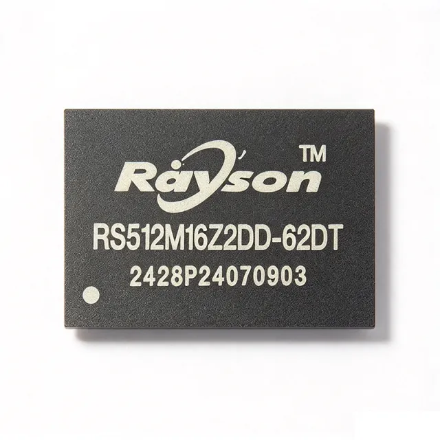
RS512M16Z2DD-62DT - 8Gbit DDR4 SDRAM 512Mx16 | Rayson
The Rayson RS512M16Z2DD-62DT is a high-performance DDR4 SDRAM (Double Data Rate Fourth Generation Synchronous Dynamic Random-Access Memory) device organized as 512M words by 16 bits, providing a total density of 8Gbit. It operates at a data rate of 3200 Mb/s/pin (DDR4-3200) with a CAS latency of 22, and is housed in a compact FBGA-96 package measuring 7.5x13 mm. This memory component is designed for mission-critical applications in industrial automation, telecommunications, edge computing, and embedded systems that require robust memory performance across extended temperature ranges. DDR4 SDRAM is the fourth generation of double data rate synchronous dynamic random-access memory, succeeding DDR3. It achieves higher speed and lower power consumption through a prefetch of 8n, a lower operating voltage of 1.2V, and improved signal integrity features such as on-die termination (ODT) and write leveling. DDR4 is a key component in modern computing systems, serving as the main memory for processors, and is also used in networking equipment, servers, and high-performance embedded designs. Key features of the RS512M16Z2DD-62DT include an operating temperature range of 0°C to +95°C, a supply voltage of 1.14V to 1.26V for VDD and 2.375V to 2.75V for VDDQ, and a clock frequency of 1.6GHz. It supports auto self-refresh, auto precharge, asynchronous reset, data mask, CRC, dynamic on-chip termination, ZQ calibration, and write leveling functions. These features ensure reliable operation and data integrity in demanding environments. The device utilizes advanced DDR4 architecture with a 16-bit I/O interface, enabling high-bandwidth data transfer. The FBGA-96 package provides excellent thermal and electrical performance, with a ball pitch that supports high-density PCB routing. The 512Mx16 organization is ideal for applications requiring large memory capacity with a moderate bus width, balancing density and pin count. Typical applications include industrial automation controllers, telecommunications infrastructure, edge computing gateways, and embedded systems that require high-speed, reliable memory. The wide temperature range and robust feature set make it suitable for harsh environments where standard commercial memory might fail. When designing with this DDR4 device, ensure proper termination and signal integrity practices are followed, including controlled impedance traces and appropriate on-die termination settings. The ZQ calibration pin must be connected to a 240-ohm resistor to ground for proper calibration.
RTS5776DL - PCIe Gen4 x4 SSD Controller | Realtek
The Realtek RTS5776DL is a DRAM-less PCIe Gen4 x4 NVMe SSD controller designed for mainstream and lower-end client solid-state drives, available in a compact BGA package. It supports four NAND channels with a 3,600 MT/s NAND interface and targets up to 7,400 MB/s sequential read/write throughput and up to 1.2 million 4K random read/write IOPS. The part is announced on Realtek's SSD controller roadmap alongside the flagship RTS5782 (PCIe Gen5) and was disclosed at Computex 2024 as a power-efficient DRAM-less option. A PCIe NVMe SSD controller is a semiconductor that bridges a host system's PCIe bus to NAND flash memory, managing protocol translation, wear leveling, bad-block management, ECC, and I/O scheduling. PCIe Gen4 x4 denotes four lanes of PCI Express generation 4, providing up to ~8 GB/s of raw host bandwidth. The Gen4 tier sits between mainstream SATA and the newer Gen5 controllers, offering a strong balance of throughput, latency, and power for client SSDs. As a sub-category, RTS5776DL belongs to the broader family of NAND flash controllers, which in turn fall under storage controllers, memory and storage ICs, and integrated circuits. Key differentiating attributes include the DRAM-less architecture (no external DDR SDRAM required, reducing BOM cost and PCB footprint), four NAND channels with 3,600 MT/s per channel toggle rate, full PCIe Gen4 x4 host interface compliance, and built-in hardware AES encryption. The DRAM-less design simplifies firmware, lowers idle power, and allows smaller M.2 2230 or M.2 2242 form-factor designs. Architecturally, the RTS5776DL integrates a multi-core processing complex paired with Realtek's in-house NAND I/O sequencer and a PCIe Gen4 physical layer. ECC options commonly support 3D TLC and QLC NAND from major vendors, with on-die temperature sensing and end-to-end data protection. Typical applications include mainstream client NVMe SSDs (M.2 2280, 2242, 2230), entry-level PCIe Gen4 SSDs targeting the upgrade market, OEM pre-installed drives in laptops and mini-PCs, portable external SSD enclosures, and DRAM-less embedded storage modules. Its low-power profile makes it attractive for thermally constrained notebooks. When designing with the RTS5776DL, careful PCB layout of the four NAND channels is critical - matched-length traces and proper decoupling prevent signal-integrity degradation at 3,600 MT/s. Thermal management should account for sustained write workloads that throttle without adequate copper pour on the host M.2 SSD PCB. This page synthesizes manufacturer roadmap disclosures, press coverage, and parametric alternatives for the RTS5776DL, including drop-in Realtek siblings and cross-brand PCIe Gen4 controllers, providing information not consolidated on any single datasheet.
RTS5782 - 14GB/s 8-Channel PCIe SSD Controller | Realtek
Realtek RTS5782 is a high-end PCIe SSD controller roadmap device featuring eight NAND channels, a 3,600 MT/s NAND interface, 4K LDPC error correction, and support for LPDDR4X cache. Published roadmap coverage associates the controller with performance targets of 14 GB/s and 2.5 million IOPS. These figures describe the announced device position and should not be treated as guaranteed production specifications until supported by an authoritative Realtek datasheet. A solid-state drive controller is a semiconductor that coordinates communication between a host interface, NAND flash, optional DRAM cache, error-correction logic, and the drive's internal data path. Within the storage-controller hierarchy, PCIe SSD controller -> storage controller -> NAND interface controller -> semiconductor, the RTS5782 is intended for high-throughput, high-end solid-state drives rather than general-purpose embedded storage. Its published eight-channel NAND architecture is designed for parallel access across multiple flash packages, while the 3,600 MT/s interface rate indicates the command-transfer rate targeted by the roadmap specification. Four-kilobyte LDPC error correction supports data-integrity requirements common in advanced NAND systems. LPDDR4X cache support can reduce direct reads of mapping metadata and improve responsiveness, although exact usable cache capacity and firmware behavior require manufacturer documentation. Typical applications include high-end client SSDs, NVMe storage systems, gaming PCs, workstations, and content-creation computers requiring fast sequential and random-access performance. The target workload benefits from multiple NAND channels and optional DRAM, but the final SSD design must still account for firmware, NAND qualification, thermal dissipation, power delivery, PCIe lane configuration, and workload endurance. A key design consideration is that the available material is roadmap-level rather than a complete production datasheet. Engineers must validate package dimensions, electrical limits, PCIe generation and lane count, supported NAND types, reference clock requirements, power rails, firmware support, and production availability with Realtek before layout release. This page separates verified published values from parameters that remain unavailable rather than estimating them.

S-25CM01A0I-J8T1U4 - 1Mbit SPI EEPROM | ABLIC Inc. | SOP-8
The ABLIC Inc. S-25CM01A0I-J8T1U4 is a 1 Mbit SPI serial EEPROM organized as 131072 words × 8 bits, housed in an 8-pin SOP (J8) surface-mount package. According to ABLIC's official datasheet, the part operates from a single 2.5 V to 5.5 V supply and supports a maximum SPI clock rate of 10 MHz, making it suitable for both 3.3 V and 5 V logic-level systems. The device offers page write and sequential read operations, hardware write-protect, and SPI modes (0, 0) and (1, 1). An EEPROM (Electrically Erasable Programmable Read-Only Memory) is a type of non-volatile memory (NVM) that retains data without power and supports byte-level in-system erase and rewrite operations. EEPROMs sit within the broader semiconductor memory hierarchy: EEPROM → non-volatile memory → semiconductor memory → integrated circuit. Unlike Flash memory, which erases in larger blocks, EEPROMs erase and rewrite at the byte or page level, making them ideal for storing configuration parameters, calibration constants, user preferences, and audit logs that change infrequently. Key features of the S-25CM01A0I-J8T1U4 include a 1 Mbit density (1048576 bits), 128K × 8 memory organization, 256-byte page write capability, write-protect (WP) hardware pin, 1 million erase/write cycles endurance per cell, and 100-year data retention. The wide 2.5 V–5.5 V supply range eliminates the need for level shifters in mixed-voltage designs, and the device's low standby current (typically < 2 µA) suits battery-powered applications. The device uses CMOS technology with a serial peripheral interface (SPI) bus, allowing compact PCB footprints and high-speed data transfer up to 10 MHz. Page write and sequential read operations enable efficient bulk data updates, while the SPI modes (0, 0) and (1, 1) ensure compatibility with most microcontroller SPI peripherals. Hardware write-protect adds safety against accidental writes in noisy environments. Typical applications include consumer electronics configuration storage, industrial sensor calibration tables, automotive infotainment settings, IoT device parameter storage, medical device patient records, and metering data logging. The 8-pin SOP package is widely available in tape-and-reel format for automated assembly. When designing with this EEPROM, ensure the SCK and CS signals have clean edges and that the WP pin is properly biased. Add a 100 nF decoupling capacitor close to VCC, and avoid long write cycles during power-down to prevent data corruption. This page synthesizes distributor pricing, same-package drop-in alternatives, and practical design notes not found in the manufacturer datasheet.

S25FL064P0XMFB003 - 64-Mbit Quad SPI NOR | Infineon
Infineon Technologies S25FL064P0XMFB003 is a 64-Mbit, 3.0 V serial NOR flash memory supporting SPI and Quad I/O at up to 104 MHz in a 16-SOIC package. The device provides 128 uniform 64-kB sectors, a 256-byte page size, and 100,000 erase-cycle endurance. According to the manufacturer data, it also uses 90 nm MirrorBit technology and is intended for embedded code storage, configuration data, firmware updates, and other nonvolatile storage applications. A serial NOR flash memory is a nonvolatile semiconductor memory device that retains stored data when power is removed. Unlike EEPROM, this device is optimized for repeated read operations and provides a compact SPI interface with optional four-lane data transfer. Its place in the memory hierarchy is below external storage such as NAND flash or disks, while its electrical density, random-access behavior, and low-latency read interface make it suitable for firmware and code execution from external flash. The S25FL064P0XMFB003 combines a 64-Mbit capacity with a 3.0 V operating class, 64-kB sector organization, and 256-byte page size. The datasheet information identifies four-kB sub-sectors within the top or bottom sectors, which can support finer selective erase workflows. Its Quad I/O interface increases transfer bandwidth compared with a single-data-line SPI connection, provided the host controller, PCB routing, and firmware support the corresponding command set. Typical applications include automotive embedded controllers, industrial equipment, consumer electronics, network appliances, and systems requiring durable nonvolatile storage for firmware, calibration data, logs, or asset records. The device can be used for code and data storage when the host processor lacks sufficient internal flash, and its sector structure allows updates at useful erase granularity rather than rewriting an entire device. Designers should verify supply voltage, command compatibility, timing, and erase endurance against the host requirements before committing a layout. The supplied data identifies the S25FL064P family as retired and recommends S25FL064L as the factory migration path, so new production designs should evaluate that superseding family before using this older device.
S25FL128P0XMFI001 - 128Mb Serial NOR Flash, 3V, 104MHz SPI | Infineon
The Infineon S25FL128P0XMFI001 is a 128-Mbit (16 MB) CMOS serial NOR Flash memory device operating from a single 2.7V to 3.6V power supply, housed in a 16-pin SOIC (300-mil) package. It provides a 104 MHz SPI (Serial Peripheral Interface) bus with the option to use single, dual, or quad I/O for higher throughput. The device organizes memory into 64 sectors of 256 KB each (or alternatively 256 sectors of 64 KB) supporting flexible erase granularity, which is a key benefit for code- and data-storage applications that require small-sector updates. A serial NOR Flash is a non-volatile memory that uses a low-pin-count synchronous serial protocol (SPI) to read, program, and erase data. NOR Flash sits at the bottom of the memory hierarchy (memory IC -> non-volatile memory -> flash memory -> NOR flash) and is preferred over NAND for random-access read workloads such as boot code, firmware images, and execute-in-place (XIP) execution, because every byte is randomly addressable with consistent, low read latency. Key specifications include a maximum SPI clock of 104 MHz in single-IO mode, page program time of approximately 1.5 ms (256 bytes), sector erase time of about 0.5 to 3.5 s for a 256 KB sector, and 100,000 program/erase cycles per sector endurance with 20-year data retention. The device supports JEDEC-standard SPI commands in addition to manufacturer-specific dual- and quad-I/O modes, and offers a hardware RESET#/WP#/HOLD# pin set for legacy compatibility. The 16-pin SOIC package is industry-standard 300-mil wide, surface-mountable, and RoHS-compliant. Architecturally, the S25FL128P uses MirrorBit technology - a NOR-compatible cell that stores two bits per cell using charge trapping rather than floating gates. This delivers higher density at lower cost than traditional NOR while preserving the byte-random read access that distinguishes NOR from NAND. The integrated 256-byte page buffer and automatic program/erase algorithms simplify firmware development. Typical applications include embedded firmware boot storage, IoT edge-node firmware update banks, automotive instrument-cluster graphics, point-of-sale terminals, industrial PLCs, set-top boxes, and consumer electronics requiring fast, deterministic code execution at power-up. The wide 2.7V-3.6V supply range also supports battery-backed designs. When designing in this part, verify that the host MCU's SPI controller can either support dual/quad mode or fall back gracefully to single-IO mode. The RESET# pin should be tied to VCC through a pull-up for robust operation; if unused, it may be left open but is recommended to be tied high to avoid spurious resets during power-up. This page synthesizes distributor pricing, drop-in alternatives, and practical design notes not found in the manufacturer datasheet, helping engineers select and qualify the S25FL128P0XMFI001 with confidence.
S25FL128SAGMFIR03 - 128Mb Quad SPI NOR Flash, 16-SOIC | Infineon
The Infineon S25FL128SAGMFIR03 is a 128 Mbit (16 Mbyte) serial NOR Flash memory organized as 16M x 8 and housed in a 16-pin SOIC (SOIC-16, 300 mil) wide-body package. It uses a standard SPI interface and supports Dual-I/O and Quad-I/O data transfer modes for throughput up to 133 MHz SDR / 80 MBps DDR, enabling execute-in-place (XiP) operation directly from external flash to reduce system DRAM cost and boot latency. What is a NOR Flash? NOR Flash is a class of non-volatile memory that allows random read access at byte granularity and supports execute-in-place (XiP), meaning the host processor can execute code directly from the flash array without first copying it to RAM. In the broader taxonomy: NOR Flash -> non-volatile memory (NVM) -> semiconductor memory -> integrated circuit. NOR Flash contrasts with NAND Flash, which is block-oriented, faster for sequential writes but slower for random reads. Because of its deterministic read latency and high reliability (typically 100k program/erase cycles and 20-year data retention), NOR Flash is the preferred boot and code-storage medium for embedded systems, automotive ECUs, and industrial controllers. Key features of the S25FL128SAGMFIR03 include 65-nm MIRRORBIT technology with Eclipse architecture, a hybrid sector architecture that combines 4 kB parameter sectors with 256 kB uniform blocks for flexible erase granularity, and an extended SPI instruction set including read, program, and erase operations. Hardware features include a hardware reset pin, a write-protect pin for block protection, a 256-byte OTP security register with a 64-byte user-programmable area, and a 128-bit Unique ID for device identification. The part supports 2.7 V to 3.6 V core supply and 1.65 V to 3.6 V I/O supply, enabling flexible interfacing with 1.8 V, 2.5 V, and 3.3 V hosts. Operating performance is anchored by a 133 MHz single-I/O SPI clock rate, Quad-SPI throughput of 80 MBps in DDR mode, and a page-program buffer of 256 bytes for efficient writes. The device sustains 100,000 program/erase cycles per sector and guarantees 20-year data retention, making it suitable for long-lifecycle industrial and automotive embedded designs. AEC-Q100 Grade 3 qualification (referenced on the Infineon part page) makes the device applicable to automotive infotainment, instrument clusters, and ADAS subsystems in addition to consumer, industrial, and networking endpoints. Typical applications include automotive infotainment and cluster boot code storage, networking switch firmware, IoT device firmware + OTA staging, industrial PLC program memory, and consumer set-top box boot loaders. Engineering tip: when laying out the PCB, keep the SCK trace length under 25 mm and place a 100 nF decoupling capacitor within 5 mm of the VCC pin to maintain signal integrity at 133 MHz. This page synthesizes distributor pricing, AEC-Q100 status, and same-footprint alternatives not found in the manufacturer datasheet alone.
S25FL256SAGNFI003 - 256Mb Quad SPI NOR Flash, 133MHz | Infineon
The Infineon S25FL256SAGNFI003 is a 256 Mbit (32 MB) serial NOR Flash memory with Quad SPI interface, operating at up to 133 MHz clock frequency in an 8-pin WSON (6x8 mm) package with exposed pad. Built on Infineon's 65 nm MirrorBit process technology, this device delivers 100,000 program/erase cycle endurance and 20-year data retention, making it a reliable non-volatile storage solution for embedded systems. A NOR Flash memory is a type of non-volatile storage that allows random byte-level read access, similar to a ROM, while also supporting in-system program and erase operations. Unlike NAND Flash, which is optimized for sequential high-density block storage, NOR Flash offers faster read access times and execute-in-place (XIP) capability, allowing microcontrollers to run code directly from the flash array. The SPI (Serial Peripheral Interface) bus reduces pin count from the parallel NOR alternative, with Quad SPI extending throughput to four bits per clock cycle for bandwidth-intensive boot and data-logging workloads. Key features include 2.7V to 3.6V single supply operation, 8 ns initial access time, hardware and software write protection, a 256-byte page programming buffer, and a 4 KB sector erase granularity with uniform 64 KB block erase support. The part supports JEDEC-standard 3-byte addressing (extendable to 4-byte via command), standard SPI (1-1-1), Dual SPI (1-1-2, 1-2-2), and Quad SPI (1-1-4, 1-4-4) modes for flexible throughput scaling. An integrated ECC engine corrects single-bit errors during page programming, raising effective yield for long-lifecycle deployments. The S25FL256SAGNFI003 is qualified across the -40C to +85C industrial temperature range and complies with MSL-3 (168-hour) moisture sensitivity, suitable for standard SMT reflow assembly. Its WSON-8 (6x8) EP package with thermal pad provides a low-profile footprint for space-constrained designs and excellent thermal dissipation for in-system reprogramming workloads. Typical applications include firmware boot storage for ARM Cortex-M/R/A microcontrollers, IoT sensor data logging, automotive infotainment (non-safety), industrial HMI panels, set-top box firmware, and wireless module configuration. The wide Quad SPI bandwidth makes it well-suited for systems requiring fast XIP code execution or rapid OTA update buffering. When designing with this device, observe the 4 KB sector erase alignment for parameter storage and use 64 KB block erase for bulk firmware updates. Place a 1uF decoupling capacitor close to VCC and follow JEDEC JESD22-A114 ESD handling protocols during board assembly. This page synthesizes distributor pricing from DigiKey, Mouser, LCSC, and Newark, plus drop-in S25FL family alternatives and practical PCB design guidance that complements the manufacturer datasheet.

S25FL512SAGBHIA10 - 512Mb Quad SPI NOR Flash 133MHz | Infineon
The Infineon S25FL512SAGBHIA10 is a 512 Mbit (64 MB) serial NOR flash memory organized as 67,108,864 bytes, housed in a 24-ball BGA (8x6 mm) package and supporting SPI, Dual SPI, and Quad SPI (Multi-I/O) interfaces at a maximum clock of 133 MHz. It is built on Infineon's 65 nm MirrorBit® technology and operates from a single 2.7 V to 3.6 V supply, providing 20-year data retention and 100,000 program/erase cycles per sector. The part is graded for the industrial temperature range (-40 °C to +85 °C) and offers uniform 256-byte page programming with built-in ECC and a 4 KB sector erase granularity. A NOR flash is a type of non-volatile memory that allows random read access at byte granularity and executes-in-place code directly from the array. In the memory hierarchy, NOR flash sits below SRAM and DRAM but above NAND flash: it is faster to read than NAND, more reliable for code storage, and uses a low-pin-count serial peripheral interface rather than a wide parallel bus. The S25FL512S fits the "serial NOR flash > NOR flash > non-volatile memory > memory IC > semiconductor" hypernymy chain and is most often deployed as the boot or firmware-storage device sitting adjacent to the host MCU/MPU. Key specifications include a 133 MHz Quad SPI clock (50 MHz single-I/O legacy), an internal 4 KB uniform sector / 256-byte page architecture, dual I/O and Quad I/O read modes, an OTP security register with a 64-byte unique ID, and a deep power-down current below 25 µA. The device supports both standard SPI mode 0/3 and a high-performance Multi-I/O mode that can sustain 80 MB/s read throughput when all four I/O lines are engaged with continuous-wrap burst reads. Program and erase are performed through a standard status-register polling mechanism or via a configurable busy/READY output. Architecturally, the S25FL512S family uses MirrorBit® charge-trap storage, which places two physically distinct bits per cell to double density without relying on smaller cell geometry. A built-in 1-bit ECC engine detects and corrects single-bit errors during page read, raising effective endurance well above the raw 100 k cycle rating. The part is fully command-set compatible with the legacy S25FL-A family and complies with JEDEC JESD216 SFDP for in-system identification of flash parameters. Typical applications include industrial gateways and PLC firmware storage, automotive infotainment boot flash, networking router boot and configuration storage, secure IoT edge nodes, and reference designs that require long-term code retention. The 24-BGA package is suited for space-constrained mobile/handheld designs where a Quad SPI interface is required to achieve the boot latency budget. Compared to NAND flash, the part executes XIP code in place and avoids ECC burden at the host. For design, place the part within 5 mm of the host with short, length-matched traces on CS#, SCK and the four IO lines, and provide a 0.1 µF plus 4.7 µF decoupling pair on VCC. Use the BGA with 0.5 mm pitch and follow standard PCB assembly guidelines for back-to-back via-in-pad if thermal cycling is expected. Hold CS# high during power-up to ensure a clean state-machine reset. This page synthesizes distributor pricing, drop-in footprint-compatible alternatives, and practical SPI flash design notes not found in the manufacturer datasheet alone.

S29AL016J70TFI010 - 16Mb 3V Parallel NOR Flash 70ns 48-TSOP | Infineon
The Infineon S29AL016J70TFI010 is a 16 Mbit (2 M x 8 / 1 M x 16) CMOS 3.0 Volt-only boot-sector NOR Flash memory in a 48-pin Thin Small Outline Package (TSOP) with 70 ns initial access time. Organized as 16 Mbit of non-volatile storage with Common Flash Interface (CFI) compatibility, the device is engineered for high-speed microprocessor-based systems requiring low-power, high-density code and data storage. A NOR Flash memory is a type of non-volatile storage that allows random access read operations, in contrast to NAND Flash which is accessed in pages. Within the semiconductor memory hierarchy, NOR Flash sits above NAND Flash and below SRAM/DRAM in the volatile-vs-non-volatile split; it is widely used for boot ROM, firmware, and execute-in-place (XIP) applications where code runs directly from flash. JEDEC-standard command sets and CFI parameters make S29AL016J70TFI010 portable across microcontrollers, embedded processors, and DSP platforms that require predictable, deterministic read latencies. Key features include ultra-low power consumption, a 20-year data retention guarantee, hardware data protection via a WP# pin, and a 70 ns access time that suits cost-sensitive embedded designs. The device supports simultaneous read/write/erase via separate banks (top or bottom boot-sector configuration) and offers sector erase granularity, enabling efficient in-application firmware updates without external buffering. The 48-pin TSOP package provides a slim 1.2 mm profile suited to space-constrained boards. Architecturally, the S29AL016J70TFI010 uses a sector-erase architecture with uniform 64 Kbyte sectors plus smaller 8 Kbyte or 16 Kbyte boot sectors, allowing fine-grained data management. The Common Flash Interface (CFI) query mechanism exposes erase/program timings and sector geometry to host software, simplifying driver portability. Hardware data protection prevents inadvertent writes, and the CMOS 3.0 V-only interface eliminates the legacy 12 V VPP requirement, enabling direct connection to modern 3.3 V microcontrollers and SoCs. Typical applications include embedded bootloader memory, automotive infotainment firmware, industrial PLCs, networking equipment, point-of-sale terminals, and consumer electronics requiring reliable non-volatile storage. The wide operating voltage range and JEDEC compatibility make it well suited to harsh-environment designs requiring long-term retention. Information sources for this component include manufacturer datasheet pages at Infineon and historical Spansion/Cypress documentation.
S29GL064S70BHI040 - 64Mb 3V Parallel NOR Flash, 70ns | Infineon
The Infineon S29GL064S70BHI040 is a 64 Mbit (8 MB) parallel NOR flash memory in the GL-S mid-density family, manufactured on Infineon's 65 nm MirrorBit process and housed in a 48-ball Fine-pitch BGA (8.15 x 6.15 mm) package. It delivers 70 ns initial access time, operates from a single 3.0 V power supply (2.7 V to 3.6 V), and supports both x8 and x16 data bus widths selected via the BYTE# input. Organized as 4,194,304 words of 16 bits or 8,388,608 bytes of 8 bits, it integrates uniform 64 KB sectors plus parameter/boot sectors with hardware sector protection. A NOR flash memory is a non-volatile storage device that connects to a microcontroller or processor via a parallel address/data bus and supports random read access at byte or word granularity - unlike NAND flash, which requires sequential page reads. The MirrorBit cell stores two bits per transistor using charge-trapping technology, doubling density versus traditional single-bit NOR without sacrificing random read speed. Within the system hierarchy, NOR flash sits between ROM (factory-programmed, immutable) and NAND flash (high-density, sequential) - offering the in-system programmability of flash with the execute-in-place capability needed to boot microcontrollers directly (XIP). Key features include a hardware sector-protection mechanism using a 128-bit protection register, a high-performance page-mode read (25 ns page access) for burst reads of up to 16 words, and an industry-standard CFI (Common Flash Interface) query that allows host software to identify geometry and timing parameters. The device supports JEDEC-standard hardware reset and offers 100,000 erase cycles per sector with a 20-year data retention rating. It is also backward-compatible with prior S29GL064N generation pinouts. Typical applications include automotive infotainment and instrument-cluster firmware storage, industrial HMI panels, networking equipment boot ROMs, point-of-sale terminals, and any embedded system requiring execute-in-place (XIP) code execution. The wide 2.7-3.6 V supply range also makes it suitable for battery-backed designs where the rail can dip toward 2.7 V at end-of-life. When designing with this part, ensure the host MCU supports the CFI query or hard-code the geometry; place a 0.1 uF decoupling capacitor within 5 mm of the VCC ball; and observe the tRPH/tWHWH1 timing parameters when migrating from S29GL064N. The BYTE# pin must be tied HIGH for x16 or LOW for x8 operation - leaving it floating is a common boot-failure cause. This page synthesizes distributor pricing, drop-in alternatives, and practical design notes not found in the manufacturer datasheet.