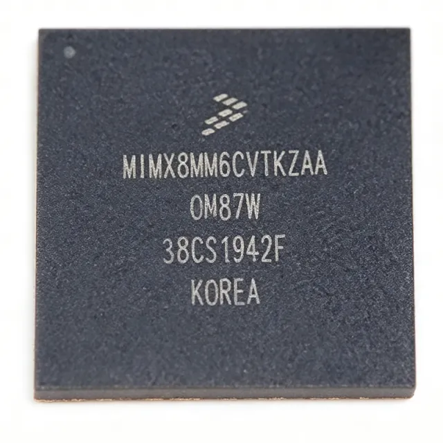
MK10DX32VMP5
MK10DX32VMP5 - 50MHz Cortex-M4 32KB MCU | NXP | 64-MAPBGA
The NXP Semiconductors MK10DX32VMP5 is a 32-bit ARM Cortex-M4 Kinetis K10 microcontroller operating at 50 MHz, with 32 KB of Flash memory, 8 KB of SRAM, and a 64-MAPBGA package measuring 5 mm by 5 mm. The verified distributor listing identifies 44 I/O pins and connectivity including I2C, IrDA, SPI, UART/USART, DMA, I2S, LVD, POR, PWM, and WDT. It is positioned as a compact, baseline, low-power MCU for space- and cost-constrained embedded systems.
A microcontroller is a programmable semiconductor system that combines a CPU core, memory, communication interfaces, timers, analog functions, and control peripherals on one integrated circuit. The MK10DX32VMP5 belongs to the ARM Cortex-M4 microcontroller family, commonly used in embedded control, motor-control, communications, and industrial systems. Its 32-bit architecture and 50 MHz operating frequency provide a practical balance between processing capability, power consumption, and integration.
Key verified features include a 50 MHz ARM Cortex-M4 core, 32 KB (32K x 8) Flash program memory, 8 KB SRAM, and a 5 x 5 mm 64-MAPBGA package. The available interface set includes I2C, SPI, UART/USART, IrDA, I2S, DMA, PWM, a watchdog timer, low-voltage detection, and power-on reset. The 44 I/O count provides connection flexibility for sensors, actuators, communications, and human-interface circuitry in compact embedded products.
The Kinetis K10 family provides a scalable entry point into the Kinetis portfolio while integrating analog, communication, timing, and control peripherals. This makes the device suitable for applications that need broad peripheral support without moving to a larger package or higher-performance MCU. Exact operating voltage, temperature range, pin assignments, flash endurance, and detailed electrical limits were not included in the supplied verified snippets and must be confirmed from the official NXP datasheet before design release.
Typical uses include low-cost industrial controllers, compact sensor nodes, communication modules, motor and motion-control subsystems, and low-power embedded products. The 64-MAPBGA footprint is especially useful where PCB area is constrained, although its fine pitch requires careful assembly and inspection processes. Designers should confirm the exact package pinout, exposed-pad requirements, power architecture, decoupling recommendations, and software support using NXP documentation.
For replacement or second sourcing, compare the complete NXP ordering information, package drawing, pin multiplexing, memory size, clock configuration, peripheral set, and software migration requirements. A part with a similar listed processor or package may not be pin-compatible or functionally equivalent. This page combines verified distributor snippets with explicit data gaps rather than estimating unavailable electrical specifications.
견적 요청
문의하기