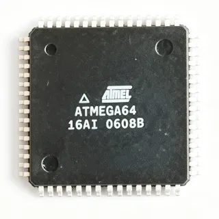
ATMEGA16-16AUR - AVR 8-Bit MCU 16MHz 16KB Flash | Microchip
부품 번호: ATMEGA16-16AUR ✓ 활성| 수량 | 단가 | 합계 |
|---|---|---|
| 1 | $9.05 | $9.05 |
| 10 | $8.32 | $83.20 |
| 100 | $7.42 | $742.00 |
| 500 | $6.65 | $3,325.00 |
| 1,000 | $5.98 | $5,980.00 |
ATMEGA16-16AUR 개요
An AVR microcontroller is an 8-bit MCU built on the enhanced AVR RISC architecture, belonging to the broader hierarchy: microcontroller -> embedded processor -> integrated circuit -> semiconductor. By executing most of its 133 powerful instructions in a single clock cycle, the ATmega16 achieves throughput approaching 1 MIPS per MHz, letting designers optimize power consumption versus processing speed.
Key features include 16 KB self-programmable FLASH, 512 B EEPROM, 1 KB internal SRAM, an 8-channel 10-bit ADC, and a JTAG interface for on-chip debugging and boundary-scan. Peripherals include two 8-bit and one 16-bit timer/counters with PWM, four USART/SPI/TWI-compatible serial interfaces, and a programmable watchdog timer with on-chip oscillator.
The advanced RISC core uses a Harvard architecture with separate instruction and data buses, enabling single-cycle instruction fetch and execution. In-System Programmable (ISP) FLASH allows firmware updates through the SPI port, while the JTAG port supports in-circuit debugging via tools such as the MPLAB SNAP.
Typical applications include industrial control panels, sensor interfaces using the 10-bit ADC, motor control PWM outputs, and hobbyist or educational embedded systems.
For design, note that 16 MHz operation is guaranteed only at 4.5 V to 5.5 V; battery-powered designs should consider the ATmega16L low-voltage grade. Decouple AVCC properly for ADC accuracy.
This page synthesizes distributor pricing, drop-in alternatives including the ATmega16A, and practical design notes not found in the manufacturer datasheet.
드롭인 대체품: ATMEGA16-16AUR — 동일 패키지, 핀 호환. PCB 재작업이 필요한 다른 패키지 부품은 제외됩니다.
이 시리즈의 변형
다음과 드롭인 호환되는 동일 시리즈 모델: ATMEGA16-16AUR (동일 폼 팩터 및 풋프린트) — 차이점: ADC, Core Architecture, EEPROM, Debug Interface, Timers/Counters.
빠른 비교 도구 — 나란히 비교할 대체 부품을 선택하십시오:
ATMEGA16A-AUR
✅ 드롭인✓ 재고 있음
$2.14 / 개
데이터시트 보기 →ATMEGA16-16AU
✅ 드롭인✓ 재고 있음
$4.41 / 개
데이터시트 보기 →ATMEGA16-16AJ
✅ 드롭인✓ 재고 있음
$2.1 / 개
데이터시트 보기 →ATMEGA16L-8AU
✅ 드롭인📋 참조 대체품 (카탈로그에 없음)
ATMEGA32A-AU
✅ 드롭인 ⚠️ 사양 미검증✓ 재고 있음
$2.95 / 개
데이터시트 보기 →ATMEGA16-16AUR 최대 정격 & 전기적 특성
| Core Architecture | AVR 8-bit RISC |
| Max Clock Frequency | 16 MHz |
| Program Memory Size | 16 KB (8K x 16) FLASH |
| SRAM Size | 1 KB |
| EEPROM Size | 512 B |
| Supply Voltage (16 MHz speed grade) | 4.5 V to 5.5 V |
| Supply Voltage (8 MHz speed grade) | 2.7 V to 5.5 V |
| 데이터 버스 폭 | 8 Bit |
| I/O Ports | 32 general purpose I/O lines |
| ADC | 8-channel 10-bit ADC |
| Timers | Two 8-bit, one 16-bit timer/counter with PWM |
| Serial Interfaces | USART, SPI, TWI (I2C-compatible) |
| Debug Interface | JTAG for on-chip debug and boundary scan |
| Instruction Set | 133 instructions, most single-cycle |
| 패키지 | 44-TQFP (10 x 10 mm) |
| 실장 유형 | Surface Mount |
| Temperature Grade | Industrial |
| Programming | In-System Programmable (ISP) via SPI |
| Watchdog Timer | Programmable WDT with on-chip oscillator |
ATMEGA16-16AUR 핀 구성
| 핀 1 | PA0 — Port A, bit 0 (ADC0 / general I/O) |
| 핀 2 | PA1 — Port A, bit 1 (ADC1 / general I/O) |
| 핀 3 | PA2 — Port A, bit 2 (ADC2 / general I/O) |
| 핀 4 | PA3 — Port A, bit 3 (ADC3 / general I/O) |
| 핀 5 | PA4 — Port A, bit 4 (ADC4 / general I/O) |
| 핀 6 | PA5 — Port A, bit 5 (ADC5 / general I/O) |
| 핀 7 | PA6 — Port A, bit 6 (ADC6 / general I/O) |
| 핀 8 | PA7 — Port A, bit 7 (ADC7 / general I/O) |
| 핀 9 | PB5 — Port B, bit 5 (MOSI / general I/O) |
| 핀 10 | PB6 — Port B, bit 6 (MISO / general I/O) |
| 핀 11 | PB7 — Port B, bit 7 (SCK / general I/O) |
| 핀 12 | RESET — Reset input (active low) |
| 핀 13 | VCC — Digital supply voltage |
| 핀 14 | GND — Digital ground |
| 핀 15 | XTAL2 — Crystal oscillator output |
| 핀 16 | XTAL1 — Crystal oscillator input / external clock |
| 핀 17 | PD0 — Port D, bit 0 (RXD / general I/O) |
| 핀 18 | PD1 — Port D, bit 1 (TXD / general I/O) |
| 핀 19 | PD2 — Port D, bit 2 (INT0 / general I/O) |
| 핀 20 | PD3 — Port D, bit 3 (INT1 / general I/O) |
| 핀 21 | PD4 — Port D, bit 4 (OC1B / general I/O) |
| 핀 22 | PD5 — Port D, bit 5 (OC1A / general I/O) |
| 핀 23 | PD6 — Port D, bit 6 (ICP1 / general I/O) |
| 핀 24 | PD7 — Port D, bit 7 (OC2 / general I/O) |
| 핀 25 | PB4 — Port B, bit 4 (SS / general I/O) |
| 핀 26 | PB3 — Port B, bit 3 (OC0 / general I/O) |
| 핀 27 | PB2 — Port B, bit 2 (AIN0 / INT2 / general I/O) |
| 핀 28 | PB1 — Port B, bit 1 (AIN1 / T1 / general I/O) |
| 핀 29 | PB0 — Port B, bit 0 (XCK / T0 / general I/O) |
| 핀 30 | NC — Not connected (per datasheet) |
| 핀 31 | AREF — ADC analog reference input |
| 핀 32 | AGND — Analog ground |
| 핀 33 | AVCC — ADC supply voltage |
| 핀 34 | PC7 — Port C, bit 7 (TOSC2 / general I/O) |
| 핀 35 | PC6 — Port C, bit 6 (TOSC1 / general I/O) |
| 핀 36 | PC5 — Port C, bit 5 (TDI / general I/O) |
| 핀 37 | PC4 — Port C, bit 4 (TDO / general I/O) |
| 핀 38 | PC3 — Port C, bit 3 (TMS / general I/O) |
| 핀 39 | PC2 — Port C, bit 2 (TCK / general I/O) |
| 핀 40 | PC1 — Port C, bit 1 (SDA / general I/O) |
| 핀 41 | PC0 — Port C, bit 0 (SCL / general I/O) |
| 핀 42 | PEN — Programming enable for serial programming |
| 핀 43 | NC — Not connected (per datasheet) |
| 핀 44 | NC — Not connected (per datasheet) |
일반적인 애플리케이션
ATMEGA16-16AUR 적합 용도: 6 애플리케이션s: Industrial Control Panels, Sensor Acquisition Systems, Motor Speed Control, Educational and Hobbyist Embedded Systems, Legacy 5V Embedded Product Maintenance, Consumer Appliance Control.
Industrial Control Panels
The ATMEGA16-16AUR fits industrial control panels because it combines a 5 V tolerant industrial-temperature AVR core, 32 I/O lines, and JTAG debugging in a single 16 MHz TQFP-44 device. Its two 8-bit and one 16-bit timers generate PWM for actuator and relay timing control, while the TWI and SPI interfaces link HMI displays, EEPROM, and RTC peripherals. The 10-bit ADC reads potentiometers and current-sense shunts at panel level, and the 16 KB FLASH retains firmware across power cycles. Placed on a 5 V rail with watchdog enabled, it provides deterministic single-cycle instruction execution for ladder-logic-style control loops at throughputs up to 16 MIPS.
추천
Sensor Acquisition Systems
The 8-channel 10-bit ADC of the ATMEGA16-16AUR makes it a natural fit for multi-channel sensor acquisition. With AVCC properly filtered and AREF decoupled, the ADC delivers 10-bit resolution (approximately 4.9 mV LSB on a 5 V reference), sufficient for temperature, humidity, and voltage-sense channels. Four ports provide 32 I/O for mux control and digital sensor buses, while USART and TWI stream readings to displays or hosts. At 16 MHz, sample loops execute with single-cycle instruction determinism, and the 512 B EEPROM stores calibration constants across power loss. The JTAG interface supports in-circuit debugging of acquisition firmware directly on the production PCB.
추천
Motor Speed Control
The ATMEGA16-16AUR suits embedded DC motor and servo speed control through its PWM-capable timers. At the 16 MHz clock, one 16-bit and two 8-bit timer/counters produce PWM carriers with up to 10-bit resolution near 15.6 kHz, above audible range for small drives. Quadrature encoder inputs are captured via port pins or counter clocking, and the 4.5 V to 5.5 V supply matches standard gate-driver logic levels. Single-cycle RISC execution ensures tight control-loop latency at up to 16 MIPS throughput. The watchdog timer with independent on-chip oscillator recovers firmware from stall faults, an important safety behavior in motor applications.
추천
Educational and Hobbyist Embedded Systems
The ATMEGA16-16AUR is widely used in universities and maker projects because it exposes classic microcontroller concepts - Harvard RISC architecture, port manipulation, timer PWM, UART, SPI, and TWI - without abstraction layers. The 16 KB ISP FLASH programs repeatedly through a simple SPI ICSP header, and JTAG allows students to step through code on real hardware using MPLAB SNAP. The DIP-compatible pin mapping on reference boards eases breadboard prototyping, while the TQFP-44 industrial part suits final builds. Its 4.5 V to 5.5 V operation matches bench supplies and legacy 5 V peripherals commonly found in teaching labs.
추천
Legacy 5V Embedded Product Maintenance
The ATMEGA16-16AUR is a preferred part for maintaining legacy 5 V embedded products still in series production. The ATmega16 family remains active, with Microchip application note AVR522 guaranteeing the ATmega16A as a functionally identical drop-in, protecting designs against process migration. Code written for the original ATmega16 runs unchanged because the instruction set, peripherals, and TQFP-44 footprint are preserved. Availability from 11 distributors as tracked by Octopart supports ongoing BOM maintenance, and the industrial temperature grade matches field equipment requirements. JTAG also permits retrofit debugging on existing PCBs without respinning.
추천
Consumer Appliance Control
The ATMEGA16-16AUR serves appliance control boards such as coffee machines, fans, and small heaters, where 5 V logic, PWM output, and a keypad interface dominate. Four 8-bit ports (32 I/O lines) drive a 4x4 keypad matrix, LEDs, and relays directly with 20 mA per-pin capability, while the 10-bit ADC reads NTC thermistors for temperature regulation. Timer PWM controls triac or MOSFET power stages at frequencies beyond audible noise. The 512 B EEPROM remembers user settings, and the programmable watchdog improves product reliability. The 16 KB FLASH holds full control firmware including UI state machines with room to spare.
추천
추천 제품 요약
엔지니어링 참조 데이터: ATMEGA16-16AUR — 비교, 설계 지침 및 규정 준수 정보.
선택 가이드
대체품과의 비교
| 파라미터 | 이 제품 | ATMEGA16A-AUR | ATMEGA16-16AU | ATMEGA16L-8AU | ATMEGA32A-AU |
|---|---|---|---|---|---|
| Package | 44-TQFP (10x10) | 44-TQFP (10x10) - same | 44-TQFP (10x10) - same | 44-TQFP (10x10) - same | 44-TQFP (10x10) - same |
| Brand | Microchip Technology | Microchip Technology | Microchip Technology | Microchip Technology | Microchip Technology |
| Max Clock Frequency | 16 MHz | 16 MHz | 16 MHz | 8 MHz | 16 MHz |
| Flash Memory | 16 KB | 16 KB | 16 KB | 16 KB | 32 KB |
| Supply Voltage Range | 4.5 V to 5.5 V (16 MHz grade) | 4.5 V to 5.5 V | 4.5 V to 5.5 V | 2.7 V to 5.5 V | 4.5 V to 5.5 V |
| SRAM | 1 KB | 1 KB | 1 KB | 1 KB | 2 KB |
| JTAG Debug | Yes | Yes | Yes | Yes | Yes |
주요 차별점
- JTAG on-chip debugging in a 44-pin TQFP (vs ATMEGA16L-8AU)
- Proven drop-in migration path (vs ATMEGA16A-AUR)
- Cost-efficient memory sizing (vs ATMEGA32A-AU)
설계 노트
Run the ATMEGA16-16AUR from a clean 4.5 V to 5.5 V rail - the 16 MHz speed grade is not guaranteed below 4.5 V per Microchip speed-versus-voltage curves. Decouple VCC with a 100 nF ceramic capacitor directly at pin 13 plus 10 uF bulk per board, and AVCC (pin 33) with its own 100 nF; connect AVCC to VCC through a low-pass LC filter (10 uH ferrite + 100 nF) for best ADC accuracy. Never let AVCC float even if the ADC is unused.
Keep the analog ground (AGND, pin 32) and digital ground connected at a single star point near the device to prevent digital switching currents from corrupting ADC readings. Route AREF (pin 31) with a short trace and 100 nF to AGND; if using the internal reference, this capacitor stabilizes it. Place the crystal and its load capacitors within a few millimeters of XTAL1/XTAL2 (pins 16/15) and guard them with ground pour to reduce jitter and EMI.
The 16 MHz operation requires the 4.5 V to 5.5 V range - powering a 16 MHz fuse-configured part at 3.3 V causes erratic execution. When migrating to ATmega16A, note AVR522 states some electrical characteristics differ due to the changed manufacturing process; re-verify marginal timing and BOD thresholds. Also remember RESET (pin 12) needs a 10 kOhm pull-up when an ISP programmer is not permanently attached, and disable JTAG via fuse if you need PC2-PC5 as general I/O.
Use the internal programmable watchdog timer with its independent on-chip oscillator as a low-cost failsafe in motor and appliance control, since it keeps running when the main clock fails. For long UART runs, keep baud rate at or below 19.2 kbps on unshielded wiring and enable the USART framing-error recovery path. External interrupt pins INT0/INT1/INT2 on PD2, PD3, and PB2 are the preferred inputs for encoder and zero-cross signals.
규정 준수 정보
RoHS-compliant lead-free TQFP per Microchip product listing; exact REACH and halogen-free statements not present in the provided data.