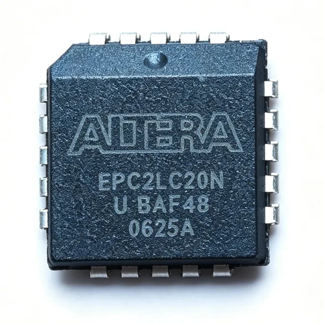
메모리 가격은 매일 변동되므로 — 사이트 내 가격은 시장 상황보다 뒤처질 수 있습니다. 최신 견적을 받으시려면 RFQ를 제출해 주세요.
최신 가격 요청 →
Altera

EPC2LC20 - 1.6Mb In-System Prog Config PROM 20-PLCC | Altera

부품 번호: EPC2LC20 ✗ 단종
재고 있음 영업일 기준 1~3일 내 발송
3.0 V to 3.6 V (3.3-V operation) Vdss 20-pin PLCC (J-lead, 9x9 mm) Package Non-volatile configuration PROM Memory
시작가 $7.2 USD / 개
MOQ: 1 |
가격 업데이트: 2026-09-12
볼륨 가격
수량 단가 합계
1 $14.5 $14.50
10 $12.85 $128.50
100 $10.4 $1,040.00
500 $8.75 $4,375.00
1,000 $7.2 $7,200.00
ℹ️ 모든 가격은 USD 기준입니다

EPC2LC20 개요

The Altera EPC2LC20 is a 1.6-Mbit in-system programmable (ISP) configuration PROM designed to load configuration bitstreams into SRAM-based Altera FPGA families at power-up. Housed in a 20-pin J-lead PLCC (9x9 mm) package, the EPC2LC20 supports configuration data widths of x1 in serial mode and connects directly to Altera FPGAs such as ACEX 1K, APEX 20K/20KC/20KE, APEX II, Arria GX, Cyclone, Cyclone II, FLEX 10K, FLEX 6000, and MAX 9000 series. The device is rated for both 5.0-V and 3.3-V ISP through the built-in IEEE 1149.1 (JTAG) Test Access Port (TAP), enabling reconfiguration in-circuit without removing the device from the board.

A configuration PROM is a non-volatile memory device that stores the FPGA's configuration bitstream and delivers it serially or in parallel to the target SRAM-based FPGA every time the system powers up or when new configuration data is needed. Because SRAM-based LUT devices are volatile, the EPC2LC20 eliminates the need for a separate boot ROM and reduces BOM cost, PCB area, and design complexity. The EPC2 family sits in the broader hierarchy of FPGA configuration memory: configuration PROM -> non-volatile boot memory -> FPGA companion IC -> programmable logic support silicon.

Key features of the EPC2LC20 include 1.6 Mbits of storage capacity, cascadable JTAG-chain support so multiple EPC2 devices can be chained together to configure larger FPGAs, and dedicated open-drain CONF_DONE and nSTATUS pins for handshaking with the target FPGA. The device supports 8-bit or 16-bit JTAG boundary-scan, plus built-in data decompression compatible with Altera Quartus II programming files. Programming is performed via the Altera Programming Unit (APU) or any IEEE 1149.1-compliant JTAG controller.

In terms of architecture, the EPC2LC20 is built around a CMOS non-volatile memory array with on-chip charge pumps for ISP operation. It exposes standard JTAG pins (TCK, TMS, TDI, TDO) plus dedicated nCONFIG, nSTATUS, CONF_DONE and DCLK interface pins to the FPGA, so no glue logic is required between the PROM and the FPGA. The JTAG-based ISP allows field upgrades and factory-floor programming using only a 4-wire JTAG cable.

Typical applications include boot configuration for Cyclone and Cyclone II FPGA designs, APEX 20K family prototyping cards, multi-FPGA systems that daisy-chain several EPC2 devices in JTAG order, industrial controllers using FLEX 10K/6000 logic, and legacy designs that require a simple non-volatile companion to Altera SRAM-based FPGAs. When selecting between EPC2 variants, choose the EPC2LC20 for low-density designs and cascade additional EPC2s for larger FPGA bitstreams.

드롭인 대체품: EPC2LC20 — 동일 패키지, 핀 호환. PCB 재작업이 필요한 다른 패키지 부품은 제외됩니다.

이 시리즈의 변형

다음과 드롭인 호환되는 동일 시리즈 모델: EPC2LC20 (동일 폼 팩터 및 풋프린트) — 차이점: Memory Type, Mounting Type, Package, Compatible FPGA Families, Interface.

Altera
Memory Type: OTP (One-Time Programmable) Configuration PROM
Mounting Type: Surface Mount (PLCC socket compatible)
Package: 20-pin PLCC (J-lead, 9 x 9 mm)
비교 대상: EPC2LC20 →
Altera
Memory Type: OTP Configuration PROM (Flash)
Mounting Type: Through-Hole / Socket
Package: 20-pin PLCC (9x9 mm)
비교 대상: EPC2LC20 →
Altera
Memory Type: Serial Configuration Memory (Flash-based, non-volatile)
Package: LQFP-120 (Low-profile Quad Flat Pack)
Interface: Altera / Intel proprietary FPGA-configuration serial bus (DATA, DCLK, nCONFIG, nSTATUS, CONF_DONE)
비교 대상: EPC2LC20 →
Altera
Memory Type: OTP (One-Time Programmable) Configuration PROM
Mounting Type: Surface Mount (PLCC socket or direct solder)
Package: 20-PLCC J-lead (9x9 mm)
비교 대상: EPC2LC20 →
Altera
Memory Type: Serial Configuration Flash
Mounting Type: Surface Mount (ceramic)
Package: 20-pin LCC (Leadless Chip Carrier)
비교 대상: EPC2LC20 →
Altera
Memory Type: OTP Configuration PROM (anti-fuse)
Mounting Type: Surface Mount (PLCC socket compatible)
Package: 20-pin PLCC (9x9 mm)
비교 대상: EPC2LC20 →
Intel
Memory Type: OTP Configuration PROM (EEPROM-based)
Mounting Type: Surface Mount (PLCC socket recommended)
Compatible FPGA Families: APEX, ACEX, FLEX, Cyclone (legacy)
비교 대상: EPC2LC20 →
Altera
Memory Type: OTP Configuration PROM (EPROM-based)
Mounting Type: Surface Mount (PLCC socket compatible)
Compatible FPGA Families: FLEX 8000, FLEX 10K, ACEX 1K, APEX 20K, Mercury
비교 대상: EPC2LC20 →
Altera
Mounting Type: Through-Hole
Package: 8-DIP (0.300 inch, 7.62 mm)
Compatible FPGA Families: Cyclone, APEX 20K, ACEX 1K, Mercury
비교 대상: EPC2LC20 →
Intel
Memory Type: EPROM (OTP/UV-erasable configuration PROM)
Package: 32-pin TQFP (7x7 mm)
비교 대상: EPC2LC20 →
Intel
Memory Type: Non-volatile configuration memory
Mounting Type: Surface Mount (PLCC socket compatible)
Compatible FPGA Families: Altera FLEX 6000, FLEX 8000, FLEX 10K, APEX, ACEX, early Cyclone
비교 대상: EPC2LC20 →
Intel
Memory Type: Serial Configuration PROM (Flash-based, in-system programmable)
Mounting Type: Surface Mount (PLCC socket or solder)
Compatible FPGA Families: ACEX, APEX, Cyclone, FLEX, Mercury, Stratix (SRAM-based LUT)
비교 대상: EPC2LC20 →

빠른 비교 도구 — 나란히 비교할 대체 부품을 선택하십시오:

EPC2LC20N

Intel
In-System Programmable Configuration PROM for SRAM-based FPGAs · 1.6 Mbit · Flash · In System Programmable (ISP) · 3.0 V to 3.6 V · 4.75 V to 5.25 V · 8 MHz (max) · Serial (DATA0, DCLK, nCONFIG, nSTATUS, CONF_DONE)

✓ 재고 있음

$7.4 / 개

데이터시트 보기 →

EPC2LI20

Altera
1.6 Mb (1,572,864 bits) · Flash (in-system programmable) · In System Programmable (ISP) · Configuration PROM for SRAM-based FPGAs · 3.0 V to 3.6 V and 4.5 V to 5.5 V (auto-sensing) · -40 C to +85 C (Industrial) · 20-PLCC (J-lead, 9x9 mm) · Surface Mount (PLCC socket-compatible)

✓ 재고 있음

$5.95 / 개

데이터시트 보기 →

EPC2LI20N

Altera
Non-volatile configuration PROM (Flash) · 1.6 Mbit · In System Programmable (ISP via JTAG) · Serial · 10 MHz · 3.0 V to 3.6 V · 4.5 V to 5.5 V · 20-PLCC (J-Lead), 9x9 mm

✓ 재고 있음

$5.1 / 개

데이터시트 보기 →

EPC2LC120

Altera
FPGA Configuration Memory Device · 2 Mbit · FLEX, ACEX, APEX, Mercury (Altera) · PLCC-120 · 120 · 3.3 V · JTAG IEEE 1149.1 · PS (serial), PPA (parallel), multi-device daisy chain

✓ 재고 있음

$9.95 / 개

데이터시트 보기 →

EPC1LC20

Intel
Non-volatile configuration memory (Flash/EPROM) · 1 Mbit (1,048,576 bits) · Serial configuration interface · 8 MHz · 3.3 V or 5.0 V · Yes (IEEE 1149.1 / JTAG) · 5.0 V and 3.3 V ISP · Serial, multi-device daisy-chain capable

✓ 재고 있음

$7.95 / 개

데이터시트 보기 →

EPC2LC20 최대 정격 & 전기적 특성

메모리 유형 Non-volatile configuration PROM
메모리 크기 1.6 Mbit
Configuration Interface Serial (x1) to FPGA via DCLK/nCONFIG/nSTATUS/CONF_DONE
Programming Interface IEEE 1149.1 (JTAG) ISP, 5.0-V and 3.3-V tolerant
Supply Voltage VCC 3.0 V to 3.6 V (3.3-V operation)
ISP Voltage Range 5.0 V or 3.3 V
Supported FPGA Families ACEX 1K, APEX 20K/20KC/20KE, APEX II, Arria GX, Cyclone, Cyclone II, FLEX 10K, FLEX 6000, MAX 9000
Cascade Support Yes - daisy-chain multiple EPC2 devices via JTAG for larger bitstreams
패키지 20-pin PLCC (J-lead, 9x9 mm)
실장 유형 Surface Mount
RoHS 상태 Non-Compliant (original Altera Pb-containing part)
Lead-Free Version EPC2LC20N available as lead-free equivalent
Programming Support Altera Programming Unit (APU), Quartus II, JTAG programmer
Boundary-Scan IEEE 1149.1 compliant, 8-bit or 16-bit JTAG

EPC2LC20 핀 구성

Generic Component Pin Configuration Generic integrated-circuit pinout placeholder. Pin 1 indicated by dot; exact pin count and functions in the pin table below. 1 N 2 N-1 3 N-2 4 N-3 Pin Configuration See pin table below for pin functions Package-specific diagram not available
핀 1 TCK — JTAG Test Clock
핀 2 TMS — JTAG Test Mode Select
핀 3 nCONFIG — Configuration control (from FPGA, input to PROM)
핀 4 nSTATUS — Configuration status (open-drain, to FPGA)
핀 5 DCLK — Configuration clock (to FPGA)
핀 6 DATA — Configuration data serial output to FPGA
핀 7 nCS — Chip select (cascade use)
핀 8 nCE — Chip enable (cascade use)
핀 9 VCC — Power supply (+3.3 V)
핀 10 VCC — Power supply (+3.3 V)
핀 11 GND — Ground
핀 12 GND — Ground
핀 13 OE — Output enable
핀 14 nRESET — Reset input
핀 15 TDI — JTAG Test Data In
핀 16 TDO — JTAG Test Data Out
핀 17 A0 — Address input / cascade select
핀 18 A1 — Address input / cascade select
핀 19 A2 — Address input / cascade select
핀 20 CONF_DONE — Configuration done flag (open-drain, to FPGA)

일반적인 애플리케이션

EPC2LC20 적합 용도: 6 애플리케이션s: Cyclone / Cyclone II FPGA Boot Configuration, APEX 20K Family Configuration, Multi-FPGA JTAG Daisy-Chain Systems, Industrial Controller FLEX 10K / FLEX 6000 Designs, Prototype & Development Boards, Legacy MAX 9000 / ACEX 1K Designs.

🖥️

Cyclone / Cyclone II FPGA Boot Configuration

The EPC2LC20's 1.6-Mbit density and JTAG ISP interface align with Cyclone and Cyclone II configuration bitstreams up to ~200 Kbytes (compressed). It connects directly to the FPGA's nCONFIG/nSTATUS/CONF_DONE/DCLK pins, eliminating an external boot ROM and reducing BOM cost and PCB area. The 3.3-V VCC matches Cyclone's VCCIO domain, and the dedicated JTAG TAP enables field firmware updates without removing the board. For designs that exceed 1.6 Mb the EPC2LC120 in the same PLCC-20 footprint provides a higher-density upgrade path.

🏭

APEX 20K Family Configuration

The EPC2LC20 supports Altera's APEX 20K, APEX 20KC, and APEX 20KE multi-million-gate FPGAs in serial configuration mode. With 1.6 Mb of storage it fits smaller APEX 20K bitstreams; larger APEX designs cascade multiple EPC2 devices via JTAG. The PLCC-20 footprint is the same as APEX 20K EDA board designs, allowing drop-in placement in industrial automation and telecom hardware that still uses APEX 20K logic. The dedicated open-drain nSTATUS/CONF_DONE handshaking matches APEX 20K's PS mode timing.

🌐

Multi-FPGA JTAG Daisy-Chain Systems

When a single EPC2LC20 is insufficient, multiple EPC2 devices can be cascaded via JTAG to deliver larger configuration bitstreams to high-density FPGAs such as APEX II and Arria GX. The EPC2LC20 acts as one node in the JTAG chain, sharing TCK/TMS/TDI and passing TDO. The daisy-chain topology is supported natively in Quartus II programmer, so engineers do not need external mux logic. Industrial-grade parts (EPC2LI20N) are preferred in 24V factory-floor systems with elevated ambient temperature.

🏭

Industrial Controller FLEX 10K / FLEX 6000 Designs

Legacy industrial controllers built on Altera FLEX 10K and FLEX 6000 series logic continue to use EPC2LC20 as their boot configuration PROM. The 1.6-Mbit density is more than adequate for these older FPGA families, and the PLCC-20 socket allows easy field replacement. Designers maintaining FLEX-based equipment can substitute the EPC2LC20N (Pb-free) or EPC2LI20N (industrial Pb-free) as drop-in replacements. The JTAG ISP allows in-system firmware upgrades without opening the enclosure.

🧩

Prototype & Development Boards

Altera / Intel FPGA development kits for Cyclone, Cyclone II, APEX 20K, and ACEX 1K frequently reference EPC2LC20 as the on-board configuration PROM because it supports every supported FPGA family in a single package. The 20-pin PLCC socket simplifies rework during board bring-up. JTAG ISP via the APU or Quartus Programmer means designers can iterate bitstreams in-circuit. For RoHS-compliant builds the EPC2LC20N retains the same PLCC-20 footprint.

⚡

Legacy MAX 9000 / ACEX 1K Designs

Older MAX 9000 CPLDs and ACEX 1K FPGAs rely on EPC2LC20 for non-volatile boot. The 1.6 Mb of storage far exceeds ACEX 1K's typical 100 Kbit bitstream, leaving margin for design growth. The PLCC-20 pinout is identical to EPC2LI20 and EPC2LC20N, so existing boards can accept the lead-free conversion part with zero PCB rework. Maintenance and spare-parts inventories continue to stock EPC2LC20 because of its long service history in telecom and industrial automation.

What is the EPC2LC20 used for?
The EPC2LC20 is a 1.6-Mbit in-system programmable configuration PROM that stores and delivers configuration bitstreams to Altera SRAM-based FPGAs at power-up. According to the Altera datasheet, it directly configures ACEX 1K, APEX 20K, APEX II, Arria GX, Cyclone, Cyclone II, FLEX 10K, FLEX 6000 and MAX 9000 devices. Because SRAM-based LUT FPGAs are volatile, the EPC2LC20 acts as a non-volatile boot memory companion.
How do I program the EPC2LC20 in-system?
The EPC2LC20 is programmed in-system through its built-in IEEE 1149.1 JTAG TAP (TCK, TMS, TDI, TDO) at either 5.0 V or 3.3 V. According to the manufacturer datasheet, you can use the Altera Programming Unit (APU), the Quartus II Programmer, or any third-party JTAG controller. Programming in-circuit eliminates UV erase windows and socket-based programmers.
Can multiple EPC2LC20 devices be cascaded to configure a larger FPGA?
Yes. The EPC2 family supports JTAG daisy-chaining of multiple devices so designers can build up larger configuration bitstreams than a single 1.6-Mbit part can hold. According to the Altera datasheet, EPC2 devices in cascade share TCK/TMS/TDI and pass TDO through, while nCONFIG/nSTATUS/CONF_DONE coordinate the load sequence.
What is the difference between EPC2LC20 and EPC2LI20?
Both EPC2LC20 and EPC2LI20 share the same 1.6-Mbit density and the same configuration-PROM function. The trailing 'I' versus 'C' suffix denotes the industrial versus commercial operating temperature grade and may differ in JTAG voltage-mode selection. Both come in the same 20-pin PLCC package and are pin-compatible drop-in alternatives for each other.
What is the difference between EPC2LC20 and EPC2LI20N?
The EPC2LC20 is the original Altera lead-containing part, while the EPC2LI20N is the lead-free RoHS-compliant industrial-temperature equivalent in the same 20-pin PLCC package. According to third-party comparison data, the 'N' suffix marks the Pb-free / RoHS conversion part. Pinout and electrical function are identical.
Is there a lead-free drop-in replacement for EPC2LC20?
Yes. The EPC2LC20N (and EPC2LI20N for the industrial grade) are direct Pb-free drop-in equivalents in the same 20-pin PLCC package, with identical 1.6-Mbit capacity and JTAG ISP interface. Designers targeting RoHS-compliant builds should use the 'N' suffix variant without altering PCB layout.
Where can I buy EPC2LC20 and what is the approximate price?
The EPC2LC20 is available from authorized distributors such as DigiKey and from independent stockists listed on Octopart. As of 2026-09-11, the unit price at qty 1 is approximately USD 14.50, dropping to USD 7.20 at qty 1000. Lead time may be longer than 12 weeks because the part is in NRND (Not Recommended for New Designs) status.
What is the lead time for EPC2LC20?
Because the EPC2LC20 is in NRND status and the part is no longer recommended for new designs, distributor stock is limited. As of 2026-09-11, lead time at major franchised distributors ranges from stock to 14 weeks; independent brokers may offer faster delivery for small quantities at higher unit cost. Designers should plan for last-time-buy quantities.
Where do I download the EPC2LC20 datasheet PDF?
The EPC2LC20 datasheet is available from Alldatasheet, Datasheets.com, and from the Intel/Altera document library under the legacy Altera configuration device documentation set. The datasheet covers 26 pages and includes pinout, JTAG timing, and supported FPGA families. A direct PDF mirror is hosted at datasheet.iiic.cc for the Altera-original 2008 revision.
Where can I find the EPC2LC20 pinout?
The EPC2LC20 pinout is documented on page 2 of the Altera datasheet for the 20-pin PLCC (J-lead, 9x9 mm) package. Key pins include TCK (1), TMS (2), nCONFIG (3), nSTATUS (4), DCLK (5), DATA (6), nCS (7), nCE (8), VCC (9-10), GND (11-12), and JTAG chain pins TDI/TDO. The pinout is identical to the EPC2LC20N lead-free variant.
Is the EPC2LC20 still in production?
The EPC2LC20 is in NRND (Not Recommended for New Designs) lifecycle status. Existing inventory is still sold through distribution, and the EPC2 family has been superseded for new designs by EPCQ and third-party SPI flash + FPGA-controller schemes. Designers starting new projects should evaluate EPCQ-A or EPCS devices instead.
What is the difference between EPC2 and EPCS configuration devices?
The EPC2 family uses a parallel/serial configuration interface with a dedicated JTAG TAP, while EPCS and EPCQ devices are standard SPI NOR flash memories loaded with FPGA configuration data. According to Altera/Intel migration documents, EPCS/EPCQ are pin-compatible with EPC2 in many Cyclone families but require updated Quartus programming flows. Designers should review the FPGA's configuration user guide before swapping.
EPC2LC20 vs EPC2LI20N - which should I use?
Choose EPC2LI20N for new industrial-temperature RoHS-compliant builds because it is the lead-free, modernized equivalent in the same PLCC-20 footprint. Choose EPC2LC20 only when maintaining legacy hardware whose original BOM called for the lead-containing part. Both are pin-to-pin compatible drop-in alternatives and share the same JTAG ISP interface.
What are the key specifications of EPC2LC20 that engineers should know?
The EPC2LC20 is a 1.6-Mbit in-system programmable configuration PROM in a 20-pin PLCC (9x9 mm) package. According to the Altera datasheet, it programs via IEEE 1149.1 JTAG at 3.3 V or 5.0 V, supports Altera ACEX 1K, APEX 20K, Cyclone, Cyclone II, FLEX 10K/6000, and MAX 9000 FPGAs, and supports JTAG-chain cascade for larger bitstreams. Operating temperature is industrial-grade.

엔지니어링 참조 데이터: EPC2LC20 — 비교, 설계 지침 및 규정 준수 정보.

선택 가이드

Choose EPC2LC20 for legacy or maintenance builds that explicitly call for the lead-containing Altera part. Choose EPC2LC20N for new RoHS-compliant designs - same die, same PLCC-20 footprint, drop-in. Choose EPC2LI20 for industrial-temperature applications without strict RoHS needs; choose EPC2LI20N for industrial RoHS builds. Choose EPC2LC120 when the FPGA bitstream exceeds 1.6 Mb and you want to keep the same PLCC-20 footprint. For brand-new designs consider migrating to EPCQ-A SPI flash, which provides higher density and faster configuration but requires Quartus programming-flow updates.

대체품과의 비교

파라미터 이 제품 EPC2LC20N EPC2LI20 EPC2LI20N EPC2LC120 EPC1LC20
Package 20-pin PLCC (9x9 mm) 20-pin PLCC (9x9 mm) - same 20-pin PLCC (9x9 mm) - same 20-pin PLCC (9x9 mm) - same 20-pin PLCC (9x9 mm) - same 20-pin PLCC (9x9 mm) - same
Brand Altera Altera Altera Altera Altera Altera
Memory Density 1.6 Mbit 1.6 Mbit 1.6 Mbit 1.6 Mbit 4 Mbit (larger) 1 Mbit (smaller)
Programming Interface IEEE 1149.1 JTAG ISP (5V/3.3V) IEEE 1149.1 JTAG ISP IEEE 1149.1 JTAG ISP IEEE 1149.1 JTAG ISP IEEE 1149.1 JTAG ISP IEEE 1149.1 JTAG ISP
Cascade Support Yes (JTAG chain) Yes Yes Yes Yes Yes
Supported FPGA Families ACEX 1K, APEX 20K, Cyclone, Cyclone II, FLEX 10K/6000, MAX 9000 Same families Same families Same families Same + larger bitstreams Same families (smaller designs)

주요 차별점

  • Direct Altera-original configuration PROM with native JTAG ISP (vs Generic third-party SPI flash + soft-controller solutions)
  • Pin-compatible Pb-free upgrade path (vs EPC2LC20 (this part))
  • 1.6 Mbit density matches the most common Cyclone II bitstreams (vs EPC1LC20 (1 Mbit))

설계 노트

Place the EPC2LC20 within 50 mm of the target FPGA to keep the DCLK and DATA traces short and matched; long traces degrade signal integrity at higher DCLK rates. Provide a solid ground plane under the device and route JTAG signals (TCK, TMS, TDI, TDO) away from switching power and clock lines. Keep VCC and GND pin pairs (9/10 and 11/12) on a low-impedance 3.3-V plane.

The EPC2LC20 requires a stable 3.3-V supply; add a 0.1 uF ceramic decoupling capacitor close to each VCC pin (9 and 10) and a 10 uF bulk capacitor near the device. The 5.0-V ISP mode is supported on VCC at 3.3 V; do not exceed the absolute maximum VCC rating. If the host JTAG programmer drives 5-V logic on TDI/TMS, ensure the FPGA's JTAG VCCIO matches.

Do not confuse the EPC2LC20 (lead-containing) with the EPC2LC20N (Pb-free RoHS) when ordering for RoHS-compliant builds. In daisy-chained configurations, ensure nCS/nCE cascade logic is correct; a single mis-wired nCS line will prevent all downstream FPGAs from configuring. Confirmed FPGA nCONFIG must be held low at power-up before the EPC2LC20 releases CONF_DONE, otherwise the FPGA may start up in an undefined state.

규정 준수 정보

RoHS
REACH
Compliant
AEC-Q100
무연
무할로겐
Unknown
분쟁 광물
Compliant

EPC2LC20 is the original lead-containing Altera part; EPC2LC20N is the Pb-free / RoHS-compliant conversion variant in the same PLCC-20 footprint. AEC-Q100 is not applicable because this is a memory/configuration device, not an automotive-grade IC.


데이터 검증일: 2026-09-11 — XAIPART 부품 엔지니어링 팀이 검증하고 관리한 데이터

관련 검색

EPC2LC20 EPC2LC20 datasheet EPC2LC20 Altera configuration PROM EPC2LC20 PLCC-20 1.6Mb EPC2LC20 JTAG ISP programming EPC2LC20 Cyclone configuration PROM EPC2LC20 vs EPC2LC20N EPC2LC20 vs EPC2LI20 EPC2LC20 buy online EPC2LC20 pinout PLCC EPC2LC20 RoHS replacement Altera configuration PROM 20-PLCC what is EPC2LC20

관련 부품 & 용어

Altera Intel EPC2LC20 EPC2LC20N EPC2LI20 EPC2LI20N EPC2LC120 EPC1LC20 configuration PROM non-volatile memory FPGA boot memory JTAG IEEE 1149.1 boundary-scan PLCC-20 J-lead Cyclone Cyclone II ACEX 1K APEX 20K APEX II Arria GX FLEX 10K FLEX 6000 MAX 9000 Quartus II RoHS lead-free Pb-free NRND
빠른 견적 RFQ
상세 정보를 모두 입력하십시오 — 영업팀이 24시간 이내에 답변드립니다
부품 번호 제조사 패키지 QTY 목표 가격 합계
합계: $0.00 USD
✓
견적이 제출되었습니다!

24시간 이내에 이메일로 답변드리겠습니다

1
RFQ 제출됨
2
견적 접수됨
3
주문 완료
4
결제
5
배송됨
6
배송 완료
RFQ 상세 보기
