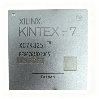
XC7K325T-1FB676I - 326,080 LE Kintex-7 FPGA | AMD | Industrial
부품 번호: XC7K325T-1FB676I ✗ 단종XC7K325T-1FB676I 개요
A field-programmable gate array is a semiconductor whose logic, memory, and I/O resources can be configured after manufacture. Within the product hierarchy, an FPGA is a programmable-logic device and a semiconductor. Compared with a fixed-function ASIC, an FPGA combines software-programmable hardware with faster design iteration, while it generally consumes more power and costs more per unit at high production volumes. The Kintex-7 family sits between lower-cost FPGA families and higher-end devices, balancing logic density, memory, programmable I/O, and signal-processing capability.
The XC7K325T-1FB676I provides 25,475 configurable logic blocks, 16,404,480 bits of block RAM, and 400 I/O according to the product listing. Its programmable I/O supports flexible interface implementation, while dedicated resources such as MMCM and PLL blocks facilitate clock generation and phase management. The large logic and memory resources allow parallel datapaths, high-throughput filtering, protocol handling, and embedded control functions to be consolidated within one device.
The -1 device designation identifies its performance class within the Kintex-7 portfolio. The industrial suffix denotes an industrial-temperature-grade configuration, although exact junction, ambient, and recommended operating limits should be confirmed in the AMD/Xilinx datasheet and package data. Package resources include numerous power and ground connections to support high-speed, high-current switching designs. The 27 mm by 27 mm FCBGA package also requires careful escape routing, controlled power delivery, and a multilayer PCB layout.
Typical applications include industrial automation controllers, high-speed data acquisition, communications infrastructure, test-and-measurement equipment, signal processing, and embedded vision systems. A designer can use the large logic fabric for parallel algorithms, block RAM for buffering or packet storage, and programmable I/O for external converters, transceivers, clocks, and high-speed memory interfaces. The architecture supports concurrent real-time processing without relying on multiple discrete programmable devices.
The primary design consideration is package complexity. A 676-ball FCBGA requires BGA assembly capability, via-in-pad or buried-via escape structures, controlled-impedance routing, and multiple power rails. Before layout, use the AMD Kintex-7 package pinout files and UG475 to verify every power, ground, configuration, clock, and user-I/O ball for the exact device suffix.
This page organizes the confirmed device identity, package, capacity, search-demand documentation queries, same-family drop-in candidates, and practical selection guidance. Exact electrical limits, configuration requirements, memory performance, and package-specific design rules should be taken directly from the current AMD/Xilinx datasheet and package documentation.
드롭인 대체품: XC7K325T-1FB676I — 동일 패키지, 핀 호환. PCB 재작업이 필요한 다른 패키지 부품은 제외됩니다.
이 시리즈의 변형
다음과 드롭인 호환되는 동일 시리즈 모델: XC7K325T-1FB676I (동일 폼 팩터 및 풋프린트) — 차이점: Speed Grade, Device Type, Package.
XC7K325T-1FBG676I
✅ 드롭인📋 참조 대체품 (카탈로그에 없음)
XC7K325T-1FFG676I
✅ 드롭인📋 참조 대체품 (카탈로그에 없음)
XC7K325T-2FBG676I
✅ 드롭인📋 참조 대체품 (카탈로그에 없음)
XC7K325T-2FFG676I
✅ 드롭인 ⚠️ 사양 미검증✗ 재고 없음
$98 / 개
데이터시트 보기 →XC7K325T-L2FBG676I
✅ 드롭인📋 참조 대체품 (카탈로그에 없음)
XC7K325T-1FB676I 최대 정격 & 전기적 특성
| Device Type | Kintex-7 Field Programmable Gate Array (FPGA) |
| Logic Elements | 326,080 |
| Configurable Logic Blocks | 25,475 |
| Total Block RAM | 16,404,480 bits |
| User I/O | 400 |
| Listed General-Purpose I/O | 250 |
| Speed Grade | -1 |
| Temperature Grade | Industrial |
| 패키지 | 676-BBGA, FCBGA |
| Package Dimensions | 27 mm x 27 mm |
| Ball Count | 676 balls |
| 실장 유형 | Surface Mount |
| Clock Management | MMCM and PLL |
| Device Family | Kintex-7 |
XC7K325T-1FB676I 27 mm x 27 mm 핀 구성 가이드
XC7K325T-1FB676I(27 mm x 27 mm 패키지)의 핀 구성입니다. 이 디지털 IC에는 GPIO, 통신 인터페이스(UART, SPI, I2C), 전원 핀이 포함되어 있습니다. 대체 핀 기능과 구성 옵션은 제조사 데이터시트를 참조하십시오. 임베디드 시스템 설계와 PCB 레이아웃에 필수적입니다.

다음에 대한 상세 핀아웃 데이터 없음: XC7K325T-1FB676I.
다음을 참조하십시오: 데이터시트 전체 핀 구성은 다음을 참조하십시오.
일반적인 애플리케이션
XC7K325T-1FB676I 적합 용도: 6 애플리케이션s: Industrial Automation and Motion Control, High-Speed Data Acquisition, Communications and Network Equipment, Test and Measurement Systems, Signal Processing and Imaging, Aerospace and Defense Control Systems.
Industrial Automation and Motion Control
The XC7K325T-1FB676I fits industrial controllers that coordinate sensors, actuators, motor-control loops, safety interlocks, and communications in one programmable device. Its 326,080 logic elements support parallel control functions, while 16,404,480 bits of block RAM can hold state, trajectory data, diagnostic records, and network buffers. The 400 user I/O provide substantial connectivity for encoders, isolated digital interfaces, analog-control systems, and field buses. In a production machine, the -1 grade supports demanding timing while the industrial designation matches extended-duty equipment. Implementation should separate deterministic I/O and clock routing, use the MMCM or PLL resources for clean internal clocks, and reserve suitable package balls for auxiliary power and ground distribution.
추천
High-Speed Data Acquisition
The XC7K325T-1FB676I is appropriate for parallel data-acquisition systems requiring real-time filtering, digital correction, buffering, and control in a single FPGA. The 400 user I/O can connect multiple converter channels, while 16,404,480 bits of block RAM provide configurable acquisition storage and digital signal-processing workspaces. MMCM and PLL resources can align converter clocks, generate deterministic sampling clocks, and manage phase relationships across parallel lanes. Using the -1 grade provides additional timing margin over lower-speed Kintex-7 options when converter sampling rates are high. The main engineering limits are the selected I/O voltage standards, achievable pin-pairs, package escape routing, and board-level channel skew. Pin assignments must be taken from the exact FB676I package files before schematic and PCB signoff.
추천
Communications and Network Equipment
The XC7K325T-1FB676I can implement high-throughput communications equipment when a design requires substantial parallel logic, packet buffering, and multiple high-speed interfaces. Its 326,080 logic elements are useful for protocol engines, classifiers, queues, and time-critical transforms, while the block RAM supports packet storage, lookup structures, and multi-port buffering. The 400 user I/O allow integration with transceivers, backplane links, clocks, and supervisory control. The -1 speed grade is advantageous for designs operating close to timing limits, although actual interface performance depends on the selected I/O standard, board topology, and device configuration. Engineers should use clock-capable pins for high-speed interfaces, preserve the required ball assignments, and validate signal integrity with the appropriate board-level constraints.
추천
Test and Measurement Systems
The XC7K325T-1FB676I supports high-end test-and-measurement systems that combine acquisition, pattern generation, real-time analysis, and instrument control in one programmable platform. Parallel logic can execute filters, correlation, digital synthesis, and error-detection algorithms, while 16,404,480 bits of block RAM can buffer captured samples or intermediate results. Its 400 user I/O provide connections to converters, calibration interfaces, trigger systems, and display or communications controllers. The -1 grade helps preserve margin in multi-clock pipelines requiring deterministic timing. Practical implementation should use dedicated clock resources, keep high-speed return paths short, and account for the FCBGA's demanding power-delivery network. Configuration retention and recovery paths should also be designed to suit the instrument's field-update requirements.
추천
Signal Processing and Imaging
The XC7K325T-1FB676I is well suited to parallel signal-processing and imaging systems that need configurable pipelines, extensive storage, and numerous external connections. Its 326,080 logic elements can implement filters, transforms, detection stages, and control logic in parallel, while block RAM stores line buffers, feature vectors, and intermediate samples. The 400 user I/O can connect image sensors, parallel ADC or DAC devices, memory components, and synchronization interfaces. The -1 performance grade provides useful timing margin for pipelined architectures, but throughput still depends on memory bandwidth and I/O rates. Designers should select the exact I/O standards early, avoid placing high-speed routes near power-distribution discontinuities, and use the package ball map to identify dedicated clock, configuration, and power connections.
추천
Aerospace and Defense Control Systems
The XC7K325T-1FB676I can serve as the programmable core in aerospace, defense, and other mission-critical control systems where high logic density, deterministic timing, and extensive I/O are valuable. Its 326,080 logic elements support redundant control paths, sensor fusion, navigation logic, health monitoring, and communication processing, while 16,404,480 bits of block RAM support local buffering and data histories. The industrial suffix identifies the listed temperature class, but a specific aerospace program must evaluate the exact ordering code, screening, qualification, and reliability requirements. The -1 grade can support demanding pipelines, provided the design meets all timing constraints. Because the package is a 676-ball FCBGA, assembly qualification, power integrity, thermal analysis, and exact package documentation are central to deployment readiness.
추천
추천 제품 요약
엔지니어링 참조 데이터: XC7K325T-1FB676I — 비교, 설계 지침 및 규정 준수 정보.
선택 가이드
대체품과의 비교
| 파라미터 | 이 제품 | XC7K325T-1FBG676I | XC7K325T-1FFG676I | XC7K325T-2FBG676I | XC7K325T-2FFG676I | XC7K325T-L2FBG676I |
|---|---|---|---|---|---|---|
| Brand | AMD | AMD | AMD | AMD | AMD | AMD |
| Package | 676-BBGA, FCBGA | 676-BBGA, FCBGA | 676-BBGA, FCBGA | 676-BBGA, FCBGA | 676-BBGA, FCBGA | 676-BBGA, FCBGA |
| Logic Elements | 326,080 | 326,080 | 326,080 | 326,080 | 326,080 | 326,080 |
| Total Block RAM | 16,404,480 bits | 16,404,480 bits | 16,404,480 bits | 16,404,480 bits | 16,404,480 bits | 16,404,480 bits |
| User I/O | 400 | 400 | 400 | 400 | 400 | 400 |
| Speed Grade | -1 | -1 | -1 | -2 | -2 | -2L |
| Clock Management | MMCM and PLL | MMCM and PLL | MMCM and PLL | MMCM and PLL | MMCM and PLL | MMCM and PLL |
| Power Class | Standard -1 grade | Standard -1 grade | Standard -1 grade | Standard -2 grade | Standard -2 grade | Low-power-screened -2L grade |
| Lifecycle Status | unknown | unknown | unknown | unknown | unknown | unknown |
주요 차별점
- Higher timing-performance class than -2 alternatives (vs XC7K325T-2FBG676I)
- Standard-grade -1 performance rather than -2L power behavior (vs XC7K325T-L2FBG676I)
- Direct same-speed family option with the G suffix (vs XC7K325T-1FBG676I)
설계 노트
Treat the 676-ball FCBGA as a demanding high-speed layout rather than a conventional fine-pitch IC footprint. Use the exact AMD package pinout files to identify power, ground, configuration, clock-capable, and user-I/O balls before assigning signals. Plan through-via or buried-via escape paths that preserve the required ball-to-trace relationship, and route high-speed differential pairs as controlled-impedance nets. Check the assembly house's pad, solder-mask, via, and X-ray inspection capabilities before schematic release.
Design a distributed power-delivery network for the device's separate supply domains rather than connecting all power balls as a single lumped rail. Follow the manufacturer package data for every VCC, VCCAUX, VCCBRAM, and ground ball, placing local decoupling capacitance at the required locations and keeping return-current paths continuous. Use plane changes and stitching vias to maintain low-impedance paths between layers. Validate the completed network with the relevant IBIS or extracted-parasitic model and check dynamic-current steps during clocking and high-speed I/O activity.
Use dedicated clock-capable inputs and the device's clocking resources for high-speed interfaces, and keep clock routing short, symmetric, and isolated from noisy data paths. Differential pairs should remain coupled without intervening layer changes or split-plane crossings, and each interface should have a clear return path. Because the package contains hundreds of balls, review every escape segment for adjacent-signal coupling before releasing fabrication data. Confirm I/O-standard, drive-strength, and slew-rate constraints against the selected speed-grade configuration.
Estimate worst-case junction temperature from actual configured logic activity, I/O toggle rates, ambient conditions, and the package's thermal model rather than from a nominal clock rate alone. The -1 grade can consume more power than lower-speed or low-power-screened Kintex-7 options, and the industrial suffix does not remove the need for thermal validation. Account for copper spreading around the BGA, internal and external board heat paths, nearby heat sources, and enclosure temperature. If margin is inadequate, reduce activity, select a lower-power speed grade, or improve the thermal design before release.
규정 준수 정보
No explicit compliance declarations for the exact XC7K325T-1FB676I orderable part were identified. Industrial-grade status is not equivalent to AEC-Q100 qualification.