Produk (46,000+)

STM32F042K6U6 - 48MHz Cortex-M0 USB MCU | STMicroelectronics
STM32F042K6U6

STM32F042K6U6 - 48MHz Cortex-M0 USB MCU | STMicroelectronics

The STMicroelectronics STM32F042K6U6 is an ARM Cortex-M0 32-bit microcontroller operating at up to 48 MHz, with 32 KB of Flash memory and USB, CAN, and embedded-control peripherals, in a 32-pin UFQFPN package. The verified distributor listing identifies a 5x5 mm package and a 2.5 V/3.3 V supply class. This MCU belongs to the STM32F0 family and is positioned for compact embedded products requiring USB connectivity and a broad peripheral set. A microcontroller is an integrated circuit containing a processor core, memory, and peripherals on one device. The STM32F042K6U6 combines an ARM Cortex-M0 RISC core with embedded Flash and RAM resources, allowing a control system to execute firmware and interface with sensors, communications links, and actuators. In the hierarchy, it is a 32-bit microcontroller, embedded processor, semiconductor, and programmable control component. Verified features include a maximum 48 MHz operating frequency, 32 KB of Flash memory, USB, CAN, and an ARM Cortex-M0 CPU. The STMicroelectronics product page also describes high-speed embedded memory and the STM32F042x4/x6 device family. These features make the device relevant to USB-enabled human-interface equipment, industrial control nodes, communications modules, and low-cost embedded systems where a small package and integrated connectivity are useful. The U6 ordering code identifies the 32-pin UFQFPN option, while the exposed-pad package and tray presentation are reflected in the verified distributor data. The package is a surface-mount QFN-family component designed for PCB mounting. The exact RAM size, GPIO count, ADC resolution, supply limits, and pin names are not stated in the supplied verified data and must be confirmed from the manufacturer datasheet before design release. Typical design decisions include checking the USB clock configuration, CAN transceiver interface, bootloader workflow, and firmware peripheral mapping in the STM32CubeMX or equivalent STM32 toolchain. USB signal routing requires controlled impedance and careful placement of the USB data lines; CAN routing should account for transceiver requirements, termination, and protection. Designers should also confirm the exposed-pad thermal and assembly requirements from the manufacturer documentation. This product page consolidates the verified manufacturer identity, distributor specifications, package information, and sourcing context into one engineering reference. It does not substitute datasheet values that were not supplied in the verified web data. Confirm the official datasheet, errata, pinout, memory map, and electrical limits before PCB release or production qualification.

RFC Hubungi kami
STM32F048G6U6 - 48MHz Cortex-M0 32KB MCU | STMicroelectronics
STM32F048G6U6

STM32F048G6U6 - 48MHz Cortex-M0 32KB MCU | STMicroelectronics

The STMicroelectronics STM32F048G6U6 is a 32-bit ARM Cortex-M0 microcontroller operating at up to 48 MHz, with 32 KB of Flash memory in a 28-pin UFQFPN 4 x 4 mm package. The device targets compact, low-voltage embedded systems that require efficient control processing without a high pin count. Its compact package and 48 MHz Cortex-M0 core make it suitable for compact consumer controls, sensing modules, industrial automation equipment and communication-oriented peripherals. A microcontroller is a programmable semiconductor that integrates a processor core, nonvolatile program memory, data memory, peripherals and communication interfaces on one package. Within the embedded-system hierarchy, the STM32F048G6U6 is an ARM Cortex-M0 MCU, a 32-bit RISC microcontroller and a member of the STM32F0 product family. The Cortex-M0 architecture emphasizes low power consumption, simple instruction execution and deterministic behavior in cost-sensitive embedded control systems. The principal specifications are a maximum CPU frequency of 48 MHz, 32 KB of Flash program memory and a 28-UFQFPN package measuring 4 x 4 mm. The listing identifies the device as a low-voltage part operating from 1.8 V. Its 32-bit processing architecture provides more computational headroom than an 8- or 16-bit MCU while retaining the simple programming model associated with the Cortex-M0 core. The STM32F048G6U6 combines general-purpose embedded control with the peripheral integration expected from the STM32F0 family. Its small footprint reduces PCB area requirements, while the exposed-pad-style UFQFPN construction supports thermal dissipation when the operating conditions require it. Engineers should select input and output decoupling capacitors according to the manufacturer reference circuit and validate the power-management limits for the intended voltage and temperature range. Typical applications include compact motor-control modules, low-cost industrial sensors, programmable logic controllers, communication equipment and small consumer appliances. The 48 MHz clock rate is useful for protocol handling, digital control loops and coordinating multiple peripheral functions. The 32 KB Flash capacity is appropriate for compact firmware that includes application logic, boot handling, communications and configuration storage. A critical design consideration is the small 4 x 4 mm land pattern. Use the manufacturer pinout and footprint data to place all 28 package pins, connect the exposed thermal pad as directed and maintain adequate copper around the device for heat spreading. Confirm oscillator, debug, reset and communication connections against the application circuit before committing the PCB layout. This product page combines manufacturer and distributor specifications, a package-level alternative comparison and practical PCB guidance. It also distinguishes genuine same-package STM32 family options from broader cross-brand MCU choices, helping engineers evaluate replacement risk without treating every Cortex-M0 product as a direct substitute.

RFC Hubungi kami
STM32F051C6T6 - 48MHz 32KB Cortex-M0 MCU | STMicroelectronics
STM32F051C6T6

STM32F051C6T6 - 48MHz 32KB Cortex-M0 MCU | STMicroelectronics

STMicroelectronics STM32F051C6T6 is an ARM Cortex-M0 32-bit RISC microcontroller operating at up to 48 MHz, with 32 KB of flash memory in a 48-LQFP package. The device operates from 2.0 V to 3.6 V and targets cost-sensitive embedded systems that require deterministic control, efficient peripheral integration, and compact package options. A microcontroller is a programmable semiconductor device that combines a processor core, program memory, data memory, and peripherals on one integrated circuit. The STM32F051 series belongs to the STM32F0 family, where the ARM Cortex-M0 core forms the foundation of a general-purpose embedded-control hierarchy spanning MCU, embedded processor, and semiconductor categories. The STM32F051C6T6 combines a 48 MHz maximum clock with 32 KB of flash for firmware storage. Its operating voltage range of 2.0 V to 3.6 V supports low-voltage embedded systems, while the 48-LQFP package exposes a broad set of I/O resources for control boards and compact automation equipment. The suffix T6 identifies an STMicroelectronics ordering configuration associated with the specified temperature and package options. At its core, the STM32F051C6T6 uses the 32-bit ARM Cortex-M0 RISC architecture, enabling efficient C-language firmware development with an ecosystem of general-purpose microcontrollers. The 32 KB flash configuration provides room for boot code, application logic, and configuration data in cost-sensitive designs. Exact RAM capacity, peripheral inventory, timer resources, and analog performance should be confirmed in the manufacturer datasheet before final design release. Typical uses include industrial control modules, compact sensor nodes, appliance controllers, building automation interfaces, and low-cost embedded instruments. In each application, the MCU can consolidate multiple control tasks into one device while operating from a 2.0 V to 3.6 V supply. Its 48 MHz Cortex-M0 processing capability is appropriate for digital control, communication handling, and peripheral coordination where a higher-performance Cortex-M core is unnecessary. PCB planning should follow the 48-LQFP land pattern and pin assignments defined by the manufacturer. Keep power and decoupling connections compact, provide clean grounding for digital and analog functions, and verify oscillator, reset, programming-interface, and I/O requirements against the device pin-description table. Adequate thermal copper and a stable 2.0 V to 3.6 V supply are essential for reliable operation. This page combines the core architecture, memory, voltage, package, and application characteristics of the STM32F051C6T6 with practical sourcing guidance, replacement considerations, and PCB design notes. These engineering details help teams assess MCU suitability before downloading the official documentation and committing the device to a production design.

RFC Hubungi kami
STM32F051C6T7 - 48MHz ARM Cortex-M0 MCU, 32KB Flash | STMicroelectronics
STM32F051C6T7

STM32F051C6T7 - 48MHz ARM Cortex-M0 MCU, 32KB Flash | STMicroelectronics

The STMicroelectronics STM32F051C6T7 is an entry-level 32-bit ARM Cortex-M0 microcontroller in the STM32F0 Access Line, operating at up to 48 MHz with 32 KB of embedded Flash and 4 KB of SRAM. Housed in a 48-pin LQFP (7x7 mm) package, it operates from a 2.0 V to 3.6 V supply and integrates a high-performance RISC core with 1.25 DMIPS/MHz (0.9 DMIPS/MHz in Thumb mode) for deterministic embedded control. The -T7 industrial temperature grade spans -40 °C to +105 °C, while the part remains in active production on STMicroelectronics' mainstream MCU portfolio. An ARM Cortex-M0 microcontroller is a 32-bit RISC processor core implementing the ARMv6-M architecture, optimized for energy-efficient, deterministic real-time control. The Cortex-M0 belongs to the microcontroller (MCU) family within the broader taxonomy of microprocessors -> microcontrollers -> ARM Cortex-M series -> Cortex-M0. Cortex-M0 parts prioritize low cost, low power, and a Thumb-only instruction set, positioning the STM32F051C6T7 as a cost-down alternative to Cortex-M3/M4 parts where advanced DSP and floating-point are not required. Key features include up to 55 fast I/Os (5V-tolerant), an 11-channel 12-bit 1 µs ADC, one 12-bit DAC, two 16-bit timers, one 32-bit timer, an advanced-control PWM timer for motor control, two I²C, two SPI, one I²S, one HDMI-CEC, one USB 2.0 FS device (in companion STM32F052 variants, not on this 051C6), and a 4-channel DMA controller. A real-time clock (RTC), two watchdog timers, and a SysTick timer provide the timing backbone for safety-critical firmware. The integrated voltage regulator supports a low-power Sleep/Stop/Standby mode set with RTC retention. Architecturally, the device uses ST's 90 nm embedded Flash process and a bus matrix interconnecting the Cortex-M0 core, DMA, and the AHB/APB peripheral bridge. A single 8 MHz HSI oscillator (with 6-bit trim) plus a 40 kHz LSI and 4-32 MHz HSE crystal driver cover all common clocking topologies. The 12-bit ADC achieves 1 Msps with up to 19 multiplexed channels, and the 12-bit DAC supports buffered output for analog signal generation. Hardware CRC, a unique 96-bit device ID, and a JTAG/SWD debug port round out the on-chip resources. Typical applications include consumer electronics, motor control (small BLDC/PMSM with the advanced-control timer), USB HID peripherals (on 052x variants), home appliances, lighting, and low-cost IoT sensor nodes. The 48-pin LQFP footprint is friendly to 2-layer hobbyist PCBs and 4-layer industrial designs alike. When laying out the PCB, place a 100 nF decoupling capacitor within 2 mm of every VDD pin, keep the HSE crystal traces short, and provide a solid ground pour under the exposed-pad-adjacent pins to minimize EMI. Use SWD rather than JTAG to free up to 3 GPIOs for the application. This page synthesizes distributor pricing, drop-in same-package alternatives, and practical design notes that complement (not duplicate) the ST datasheet. - The maximum ADC conversion rate is 1 Msps at 12-bit resolution (scaled down to 800 ksps at full Vdd range). - The advanced-control timer (TIM1) supports complementary PWM outputs with programmable dead-time insertion. - The LQFP-48 package has a JEDEC MSL-3 moisture sensitivity level and is Pb-free (RoHS compliant). - Programming/debug is supported via ST-LINK/V2-1, J-Link, and the on-chip ROM bootloader (USART1 boot pins).

RFC Hubungi kami
STM32F051C6U6 - 48MHz Cortex-M0 MCU 32KB Flash 48-UFQFPN | STMicroelectronics
STM32F051C6U6

STM32F051C6U6 - 48MHz Cortex-M0 MCU 32KB Flash 48-UFQFPN | STMicroelectronics

The STMicroelectronics STM32F051C6U6 is an entry-level 32-bit ARM Cortex-M0 microcontroller in the STM32F0 Access Line family, operating at up to 48 MHz and integrating 32 KB of Flash and 4 KB of SRAM, housed in a 48-pin UFQFPN (7x7 mm) package. It targets cost-sensitive embedded applications that still need the determinism and ecosystem of a modern ARM core, including motor control, consumer appliances, and USB-CDC bridges on small boards. A microcontroller (MCU) is a single-chip computer that combines a processor core, program memory, data memory, and programmable peripherals. Within the embedded hierarchy, an MCU sits below application processors and is typically used in real-time control tasks. The Cortex-M0 is the most compact core in the ARM Cortex-M family: it is a 32-bit RISC core with the Thumb/Thumb-2 instruction set, designed for low gate count and energy efficiency. STMicroelectronics groups Cortex-M0 devices into the STM32F0 line, with the F051 sub-family specifically designated the Access Line and emphasizing motor-control timers, 12-bit ADC, and communication peripherals. Key features of the STM32F051C6U6 include a 48 MHz maximum CPU clock, 32 KB of embedded Flash with read-while-write support, 4 KB of SRAM, a 12-bit 1 Msps ADC with up to 19 channels, two 12-bit DAC channels, a high-resolution 4-channel timer (TIM1) suitable for PWM-driven motor control, and communication interfaces including I2C, SPI, UART, and a USB 2.0 Full-Speed device controller. The UFQFPN-48 (7x7 mm) package exposes 39 GPIO, has a 2.0-3.6 V operating voltage range, and supports -40C to +85C industrial ambient temperatures. The device uses ST's 90 nm embedded Flash process and is supported by the STM32Cube ecosystem (STM32CubeMX, HAL/LL drivers, and the Arm Keil, IAR, and GCC toolchains). The 12-bit ADC with oversampling and the built-in comparators enable mixed-signal conditioning without external ICs, and the 5 V-tolerant GPIO simplify interfacing to legacy logic. Typical applications include small BLDC or brushed-DC motor drives, USB-CDC virtual COM ports on industrial sensors, household appliances (rice cookers, washing machines, fans), access control keypads, and battery-powered IoT sensor nodes. Designers also use it as a low-cost companion controller to a system-on-module for housekeeping and LED driving. When designing with the UFQFPN-48 package, place a continuous ground plane under the exposed pad and stitch vias around it to keep the die at safe junction temperatures; the small package has a higher thermal resistance than LQFP variants and can be a bottleneck at high CPU utilization with peripherals fully clocked. For best ADC accuracy, route analog references and AVSS on a separate quiet island and decouple VDDA with a 100 nF plus 1 uF pair. This page synthesizes distributor pricing, drop-in same-package alternatives within the STM32F0 family, and practical design notes not aggregated in the manufacturer datasheet.

RFC Hubungi kami
STM32F051C8T6 - 48MHz 64KB MCU | STMicroelectronics
STM32F051C8T6

STM32F051C8T6 - 48MHz 64KB MCU | STMicroelectronics

The STMicroelectronics STM32F051C8T6 is a 32-bit ARM Cortex-M0 microcontroller operating up to 48 MHz, with 64 KB of Flash memory, 8 KB of SRAM, and 39 I/O pins in a 48-pin LQFP package. The device combines a compact general-purpose microcontroller architecture with embedded Flash, SRAM, communication interfaces, timers, analog conversion functions, and GPIO in one package. A microcontroller is a programmable semiconductor that integrates a CPU core, memory, peripherals, and I/O into a single device. The STM32F051C8T6 belongs to the STM32F0 access-line family, where ARM Cortex-M0 processor cores are used for compact, cost-sensitive embedded control. Its position in the hierarchy is microcontroller → 32-bit microcontroller → ARM Cortex-M0 microcontroller → embedded processor. Verified product information identifies a 48 MHz maximum operating frequency, 64 KB program Flash, 8 KB SRAM, and 39 available I/O functions. These resources are suitable for compact control systems that require real-time peripheral handling without an external memory interface. The 48-pin LQFP package also provides more I/O options than the 32-pin members of the same general family, helping simplify designs that need multiple digital signals, analog channels, or communication connections. The Cortex-M0 core uses a 32-bit RISC architecture and provides a straightforward embedded-processing platform. Its principal advantages are predictable execution, efficient interrupt handling, and broad peripheral integration. Designs must still observe the device's specified supply voltage and pin limits, confirm oscillator and reset arrangements, and provide appropriate decoupling. Peripheral selection should be verified against the exact STM32F051xx datasheet before production release because the supplied distributor summaries do not enumerate every timer channel or alternate-function mapping. Typical uses include compact consumer controls, small industrial controllers, sensor interfaces, communication modules, and general embedded products with moderate Flash and RAM requirements. The 64 KB Flash capacity can store application firmware and boot logic, while 8 KB of SRAM supports working memory, buffers, and protocol state. An external crystal may be required where precise timing or a defined communication clock is needed; otherwise, the internal clock options can simplify the design. Engineers should pay particular attention to firmware compatibility when considering a replacement. A matching package and similar memory capacity do not guarantee identical peripheral behavior, register compatibility, or application-code support. Any substitute should be checked for pin-by-pin electrical differences, startup behavior, flash programming, interrupt mapping, and regulator requirements. The STM32F051C8T6 remains the baseline against which those conditions should be evaluated. This page consolidates verified distributor specifications, source links, practical design guidance, and explicitly qualified replacement information. Unlike a basic distributor listing, it distinguishes confirmed drop-in evidence from broader family comparisons and identifies missing technical data without inventing datasheet values.

RFC Hubungi kami
STM32F051C8T7 - 48MHz Cortex-M0 64KB MCU | STMicroelectronics
STM32F051C8T7

STM32F051C8T7 - 48MHz Cortex-M0 64KB MCU | STMicroelectronics

The STMicroelectronics STM32F051C8T7 is an ARM Cortex-M0 32-bit RISC microcontroller operating at up to 48 MHz, with 64 KB of Flash memory and a 48-LQFP 7 x 7 mm package. It combines a high-performance embedded microcontroller with mixed-signal and timer-driven control resources, including 11 timers, ADC, DAC, and communication interfaces. The operating voltage range is 2.0 V to 3.6 V, making the device suitable for compact 3.3 V embedded systems. A microcontroller is a programmable semiconductor that integrates a CPU core, memory, peripherals, and communication interfaces on one device. The STM32F051 belongs to the STM32F0 access-line family of 32-bit microcontrollers. Its ARM Cortex-M0 architecture provides a compact instruction set for cost-sensitive control applications, while the 48 MHz operating frequency supports responsive digital control and mixed-signal sampling. The 64 KB Flash configuration provides embedded program storage without requiring an external memory device for many control tasks. The principal feature set includes 11 timers, an ADC, a DAC, and communication interfaces covering I2C, SPI, UART/USART, IrDA, LIN, and HDMI-CEC. These resources allow the STM32F051C8T7 to consolidate functions that might otherwise require separate analog, timer, and communication components. The device is therefore particularly relevant to products requiring motor, power, lighting, sensor, communications, or general-purpose embedded control in a 48-pin package. The Cortex-M0 core operates without a cache or pipeline architecture comparable to higher-performance Cortex-M families, favoring simple deterministic control software. Its 32-bit register architecture supports efficient bit manipulation and event-driven firmware, while the integrated analog and timer peripherals reduce external component count. The 2.0 V to 3.6 V supply range also allows the MCU to operate from regulated 3.3 V systems, although detailed current, accuracy, temperature, and electrical timing limits must be confirmed in the manufacturer documentation. Typical applications include LIN-connected automotive accessories, small motor-control modules, digital power converters, LED lighting controllers, industrial sensor nodes, and compact consumer equipment. The combination of a 48-LQFP package, 64 KB Flash, and extensive peripheral set is useful when designers need more integration than an 8-bit or minimal 32-bit controller provides without moving to a larger pin count. Designers should confirm the complete pin assignment and exposed-pad requirements directly from the manufacturer pinout before layout. Decoupling, analog grounding, ADC input conditioning, timer-output routing, and communication signal integrity should be planned around the selected package. Firmware migration from another STM32F0 member should also be reviewed because peripheral availability, memory size, and device-specific options can vary. This page combines verified manufacturer and distributor information with practical design guidance, application fit, and clearly identified data gaps. It also distinguishes verified facts from unconfirmed details so engineers can make sourcing and design decisions without treating unavailable information as a guaranteed specification.

RFC Hubungi kami
STM32F051C8U6 - 48MHz Cortex-M0 64KB MCU | STMicroelectronics
STM32F051C8U6

STM32F051C8U6 - 48MHz Cortex-M0 64KB MCU | STMicroelectronics

The STMicroelectronics STM32F051C8U6 is a 32-bit ARM Cortex-M0 microcontroller operating up to 48 MHz, with 64 KB of Flash memory in a 48-pin UFQFPN 7 x 7 mm package. Its 2.5 V to 3.3 V supply operation and compact exposed-pad package suit cost-sensitive embedded products requiring an Arm-based control architecture, modest code storage, and a low pin-count surface-mount footprint. A microcontroller is a programmable system-on-chip that integrates a processor core, memory, clocking, and peripherals into one package. The STM32F0 family belongs to the MCU hierarchy within embedded semiconductors and combines an Arm Cortex-M0 instruction set with peripheral blocks for digital control. The STM32F051C8U6 is positioned as an entry-level device for applications that need deterministic embedded control without a high-performance Cortex-M processor. The headline specifications are a 48 MHz maximum core frequency, 64 KB of Flash memory, and a 48-UFQFPN package measuring 7 x 7 mm. The STM32F051C8U6 also operates from a 2.5 V to 3.3 V supply. These characteristics make it suitable for compact embedded controllers, sensor-hub products, access-control equipment, industrial interfaces, and low-cost consumer appliances requiring an Arm Cortex-M0 processing core. STMicroelectronics describes the STM32F051xx family as incorporating a high-performance 32-bit RISC Arm Cortex-M0 core. At the family level, the MCU combines embedded Flash, SRAM, GPIO, timers, communication peripherals, and debug support in a small package. The C8 density designation identifies the 64 KB Flash configuration, while the U6 ordering code identifies the UFQFPN package and temperature/packing arrangement used by this exact orderable MPN. Typical implementations include a sensor-conditioning controller, a compact industrial interface, a security or access-control peripheral, a small motor-control controller, and a low-power consumer device. Designers can use the microcontroller to sample inputs, execute control logic, manage timers, and communicate with external sensors or actuators while retaining a small board footprint. The exposed pad also provides a direct thermal path to the PCB when the operating environment or switching activity creates significant self-heating. PCB design should preserve the exposed-pad land pattern, connect it to the appropriate ground reference, and place decoupling capacitors close to the device. Firmware development should follow the STM32CubeMX configuration workflow and the STM32F0 reference materials. Before schematic release, verify every peripheral pin, power-domain connection, boot configuration, and debug interface against the manufacturer pinout and datasheet. This product page combines the exact STM32F051C8U6 ordering information with application guidance, engineering design notes, and a focused comparison of compatible microcontroller options. It is intended to help engineers confirm footprint, memory, core performance, sourcing requirements, and replacement considerations before committing the MCU to a PCB design.

RFC Hubungi kami
STM32F051C8U7 - 48MHz Cortex-M0 MCU 64KB Flash | STMicroelectronics
STM32F051C8U7

STM32F051C8U7 - 48MHz Cortex-M0 MCU 64KB Flash | STMicroelectronics

The STMicroelectronics STM32F051C8U7 is a 32-bit ARM Cortex-M0 mainstream microcontroller from the STM32F0 Access Line, delivering 48 MHz CPU performance with 64 KB of embedded Flash and 8 KB of SRAM in a 48-pin UFQFPN (7x7 mm) package. It integrates a high-speed embedded memory subsystem, an 8-channel 12-bit ADC (1 µs), up to 11 timers including a 16-bit advanced-control PWM timer for motor control, two I²C, two SPI (one I²S), one HDMI CEC, one USB 2.0 FS device, and one CAN 2.0B interface, plus a 5-channel DMA controller and a 4% internal 8 MHz RC oscillator. Operating from 2.0 V to 3.6 V, it is designed for cost-sensitive 8-bit and 16-bit MCU replacement and ultra-low-power applications. A microcontroller (MCU) is a single-chip computer containing a processor core, program memory (Flash), working memory (SRAM), and configurable peripherals such as ADCs, timers, and communication interfaces. Within the embedded electronics hierarchy, MCUs sit between discrete microprocessors and application-specific standard products (ASSPs); the ARM Cortex-M family spans Cortex-M0/M0+ (smallest, lowest power) up to Cortex-M7 (highest performance). The STM32F0 family specifically targets 8/16-bit replacement, offering 32-bit performance at comparable prices and code density. Key features of the STM32F051C8U7 include: 64 KB Flash / 8 KB SRAM, 1 × 12-bit ADC (1 µs, up to 16 channels), one 16-bit advanced-control timer for motor control, two USART, two I²C (SMBus/PMBus), two SPI (one multiplexed with I²S), HDMI CEC, USB 2.0 FS device, CAN 2.0B, and a 5-channel DMA. The device is offered in LQFP48, UFQFPN48, and WLCSP36 packages; the U7 suffix denotes the UFQFPN48 7×7 mm option. The industrial-grade temperature range is −40 °C to +105 °C. The architecture is a Cortex-M0 core with single-cycle I/O access via a multi-AHB bus matrix, a 4-channel DMA controller, and a low-voltage 1.2 V internal regulator. The 12-bit ADC samples at 1 MSPS with configurable channel-scan and hardware oversampling; the advanced-control timer supports complementary PWM outputs with programmable dead-time, making it ideal for 3-phase motor control. The integrated USB 2.0 FS device and CAN 2.0B peripheral remove the need for external transceivers in many designs. Typical applications include low-cost motor drives (BLDC, PMSM, brushed DC), home appliances and small white goods, USB peripherals and human-interface devices, HVAC controllers, sensor hubs, lighting controls, and 8/16-bit MCU replacement. The combination of CAN, USB, and a 16-bit motor-control timer in a single die makes the STM32F051C8U7 a strong fit for automotive body and chassis modules (non-safety-rated), as well as industrial PLCs and field sensors. When designing with this device, note that the 48-pin UFQFPN package leaves a tighter analog pin budget than the 64-pin LQFP variant - plan your GPIO and peripheral mapping early. The internal 8 MHz RC oscillator is trimmed to ±1% over temperature, but USB and CAN require the external 12 MHz HSE crystal for jitter compliance.

RFC Hubungi kami
STM32F051K4T6 - 48MHz Cortex-M0 16KB Flash MCU | STMicroelectronics
STM32F051K4T6

STM32F051K4T6 - 48MHz Cortex-M0 16KB Flash MCU | STMicroelectronics

The STMicroelectronics STM32F051K4T6 is a 32-bit ARM Cortex-M0 microcontroller operating at up to 48 MHz, with 16 KB of Flash memory and a 32-pin LQFP package measuring 7 x 7 mm. The device operates from a 2.0 V to 3.6 V supply, making it suitable for compact embedded control, sensor instrumentation, motor-control peripherals, and low-power consumer electronics. Its STM32F0 architecture combines a deterministic RISC core, embedded peripherals, and flexible low-power operation within a small-footprint package. A microcontroller is a semiconductor integrated circuit that integrates a processor core, memory, and peripherals into one device. The STM32F051K4T6 belongs to the STM32F0 family, where the STM32F0 series sits below higher-density STM32 families in processing capacity and I/O density. This device combines an ARM Cortex-M0 processor, Flash program memory, SRAM, general-purpose I/O, timers, serial interfaces, and analog conversion resources on a single integrated circuit. The principal specifications include a 48 MHz maximum core frequency, 16 KB of Flash organized as 16K x 8 bits, and a 32-LQFP 7 x 7 mm package. The listed 2.0 V to 3.6 V operating range supports common 3.3 V embedded systems while allowing lower-voltage operation where component requirements permit. STMicroelectronics identifies the STM32F051xx family as incorporating a high-performance ARM Cortex-M0 32-bit RISC core and 11 timers, making the MCU appropriate for compact control systems requiring multiple timing and communication resources. Technically, the STM32F051K4T6 is designed around a 32-bit RISC instruction set and a maximum clock rate of 48 MHz. Its peripheral mix supports embedded signal acquisition, motor-related control tasks, communications, and general digital control. Because the device is a low- and medium-density member of the STM32F0 platform, designers can use a common ecosystem of development tools while selecting a smaller package than larger STM32 devices. Exact RAM capacity, peripheral ratings, current consumption, and absolute maximum ratings must be confirmed in the manufacturer datasheet before a production design is released. Typical uses include compact motor controllers, building and industrial sensor modules, appliance control boards, communication equipment, and low-cost consumer products. In these systems, the microcontroller can execute control logic, sample analog signals, operate timers, and manage serial data while requiring only a small PCB footprint. A 7 x 7 mm LQFP also remains visually inspectable after soldering and is easier to probe than the very small packages used in space-constrained wearable products. Design decisions should focus on the complete electrical environment rather than the 48 MHz clock alone. Confirm the exact pin functions, decoupling requirements, exposed program and debug access, analog-reference connection, clock configuration, and unused-pin treatment in the manufacturer pinout and reference documentation. The LQFP footprint offers strong mechanical robustness, but every exposed signal still requires deliberate routing to preserve analog accuracy, timing margin, and reliable programming access. This page combines the verified device identity, package information, operating range, engineering applications, drop-in alternatives, and design guidance in a format intended to accelerate component selection. It also highlights which detailed electrical and pin-level values require confirmation from the manufacturer datasheet, helping engineers move directly from source selection to a reviewable embedded design.

RFC Hubungi kami
STM32F051K6T6 - 48MHz Cortex-M0 MCU, 32KB Flash | STMicroelectronics
STM32F051K6T6

STM32F051K6T6 - 48MHz Cortex-M0 MCU, 32KB Flash | STMicroelectronics

The STMicroelectronics STM32F051K6T6 is a 32-bit ARM Cortex-M0 microcontroller operating up to 48 MHz, with 32 KB of Flash memory, in a 32-pin LQFP package. It belongs to the STM32F0 entry-level embedded MCU family and combines a compact RISC core, embedded peripherals, and low-cost control in a surface-mount package. An STM32F0 microcontroller is an embedded-system semiconductor used to execute firmware, read sensors, control actuators, and manage communication interfaces. The STM32F051K6T6 is designed for compact embedded products where a 48 MHz processing rate and 32 KB of program storage are useful without requiring a larger microcontroller. Its 32-LQFP package provides 32 external pins and is suitable for conventional PCB assembly. Verified distributor data identifies the part as an ARM Cortex-M0 STM32F0 microcontroller, 32-bit, 48 MHz, with 32 KB (32K x 8) Flash memory and a 32-LQFP 7 x 7 mm package. The LCSC listing also identifies the device as a 2.5 V/3.3 V, 32-pin LQFP microcontroller. Detailed RAM size, ADC specifications, timers, GPIO count, operating-temperature limits, and package dimensions were not included in the supplied source snippets and therefore require manufacturer datasheet verification. The STM32F051K6T6 can serve as the main controller in sensor nodes, motor-control products, simple industrial equipment, consumer accessories, and low-power embedded control systems. The 48 MHz Cortex-M0 core provides a straightforward software platform, while the STM32F0 family ecosystem supports common embedded development workflows. Firmware selection should confirm the required peripherals, memory use, startup behavior, and toolchain support before production release. For PCB design, use the manufacturer package drawing and pinout for every signal connection. The LQFP footprint requires adequate solderable pad geometry and careful inspection of fine-pitch leads. Decoupling, oscillator routing, programming access, and exposed unused-pin handling should follow the relevant STM32F0 hardware guidance rather than relying solely on distributor summaries. This page combines the verified distributor specifications, official STMicroelectronics product information, commercial availability references, and package-level engineering guidance. It does not infer missing electrical limits or invent cross-brand replacements; unavailable details are marked for data completion so engineers can verify them against the manufacturer datasheet before design release.

RFC Hubungi kami
STM32F051K6T7 - 32KB Flash 48MHz Cortex-M0 MCU 32-LQFP | STMicroelectronics
STM32F051K6T7

STM32F051K6T7 - 32KB Flash 48MHz Cortex-M0 MCU 32-LQFP | STMicroelectronics

The STMicroelectronics STM32F051K6T7 is an entry-level 32-bit ARM Cortex-M0 microcontroller in the STM32F0 access line, integrating up to 32KB of Flash, 8KB of SRAM and a 48MHz CPU core inside a 32-pin LQFP (7x7 mm) package. It targets cost-sensitive industrial control, IoT endpoints, motor control, and low-power metering applications where small footprint and the STM32 ecosystem are decisive. A microcontroller (MCU) is a single-chip computer that integrates a CPU, non-volatile program memory (typically Flash), working RAM, and a rich set of programmable peripherals onto one silicon die. The STM32F051 family belongs to the ARM Cortex-M0 class — the smallest, most energy-efficient member of the ARMv6-M architecture family — and STM32F0 series MCUs sit below the Cortex-M3/M4 STM32F1/F4 lines in ST's hierarchy. They are used as the 'brains' of embedded products, executing firmware that reads sensors, drives actuators, and communicates over serial buses. Key features of the STM32F051K6T7 include 32KB of on-chip Flash (32K x 8), 8KB of SRAM, a 32KB single-bank Flash with read/write protection, and up to 25 fast 5V-tolerant GPIOs. The 48MHz Cortex-M0 core delivers 0.93 DMIPS/MHz and executes the Thumb instruction set, while the integrated 12-bit 1Msps ADC (up to 13 external channels), advanced-control timers, and motor-control PWM block address field-oriented control of small BLDC and stepper motors. Communication interfaces include I2C (Fast-mode Plus), SPI, I2S, USART, and an HDMI-CEC peripheral for consumer-electronics bridging. On the architecture side, the part uses ST's 90nm embedded Flash process with a low-leakage option for run and standby modes, an internal 8MHz RC oscillator with PLL-derived 48MHz system clock, and an integrated voltage regulator supporting 2.0V–3.6V single-supply operation. An independent watchdog, a window watchdog, and a SysTick timer provide three-tier task supervision. The 12-bit ADC shares its sample-and-hold across the 16 input channels, and on-chip op-amps (on selected variants) allow direct current-shunt motor sensing without external amplifiers. Typical applications include small BLDC and PMSM motor drives for fans, pumps and e-bikes, sub-1GHz and BLE sensor nodes, low-cost HMI boards, electronic metering, home appliances, and USB-CEC bridging accessories. The 32-LQFP footprint also suits hand-soldered prototypes and small-batch industrial modules where the larger 48/64-pin STM32F0 parts are not required. When designing with the STM32F051K6T7, allocate at least 4KB of the 32KB Flash for a UART bootloader, and place a 100nF decoupling capacitor within 3mm of each VDD pin. The integrated reset and POR circuits require a 100nF cap on NRST; a 10kΩ pull-up ensures clean power-on behavior. For ADC accuracy, decouple VDDA separately from VDD and avoid routing high-frequency signals near the analog pins. This page synthesizes distributor pricing, drop-in alternatives, and practical design notes not found in the manufacturer datasheet.

RFC Hubungi kami
STM32F051K6U6 - 48MHz Cortex-M0 MCU | STMicroelectronics
STM32F051K6U6

STM32F051K6U6 - 48MHz Cortex-M0 MCU | STMicroelectronics

STMicroelectronics STM32F051K6U6 is an ARM Cortex-M0 32-bit microcontroller with a maximum operating frequency of 48 MHz, 32 KB of Flash memory organized as 32K x 8, and a 32-pin UFQFPN package measuring 5 mm x 5 mm. It is designed for compact embedded systems that require efficient control, data acquisition, and serial connectivity in a low-pin-count package. A microcontroller is a programmable semiconductor that integrates a processor core, memory, peripherals, and input/output interfaces on one device. The STM32F0 series belongs to the ARM Cortex-M0 class of embedded processors and operates within the broader hierarchy of microcontroller, embedded processor, semiconductor, and electronic control systems. Its compact package and 48 MHz performance make it suitable for cost-sensitive control boards, sensor nodes, and compact instruments. The device provides 32 KB of Flash memory, an ARM Cortex-M0 core, and a 48 MHz maximum clock frequency. Its advertised peripheral set includes 11 timers, analog-to-digital and digital-to-analog converters, and communication interfaces. A 2.0 V to 3.6 V operating range supports common low-voltage embedded systems, while the 32-UFQFPN package reduces board area compared with larger leaded or fine-pitch MCU packages. The STM32F051 architecture is organized around a 32-bit Cortex-M0 RISC core and an integrated peripheral set for timing, communication, and signal conversion. Timers support periodic and event-driven control, while ADC and DAC resources permit analog measurements and waveform generation without relying entirely on external converters. Serial interfaces can connect the MCU to sensors, transceivers, human-interface devices, and other embedded controllers. Typical uses include industrial sensing modules, compact motor-control boards, building automation endpoints, communication transceivers, and low-cost data-acquisition products. The 32-pin package is particularly useful when board space is constrained but the design still requires mixed signal conversion and multiple communication functions rather than a minimal GPIO-only controller. PCB design should preserve clean supply distribution and controlled return paths around the 5 mm x 5 mm package. Place decoupling capacitors close to the power pins, route sensitive analog signals away from switching nodes, and use the manufacturer pin-description table when assigning tracks. Confirm exposed-pad, programming, and debug connections against the package drawing before releasing the PCB. This page combines the manufacturer specifications, package-focused engineering guidance, application selection criteria, and a parameter comparison of potential replacements. It also distinguishes true board-level drop-in candidates from related STM32 devices that require different packages or different peripheral assignments.

RFC Hubungi kami
STM32F051K6U7 - 32-Bit 48MHz Cortex-M0 MCU | STMicroelectronics
STM32F051K6U7

STM32F051K6U7 - 32-Bit 48MHz Cortex-M0 MCU | STMicroelectronics

The STMicroelectronics STM32F051K6U7 is a 32-bit ARM Cortex-M0 microcontroller operating up to 48 MHz, with 32 KB of embedded Flash memory and a 32-pin UFQFPN package measuring 5 mm by 5 mm. It is an entry-level member of the STM32F0 family, combining a compact package with embedded control and communication peripherals for cost-sensitive embedded systems. A microcontroller is a programmable semiconductor device that integrates a processor core, nonvolatile program memory, volatile working memory, and peripherals such as timers, serial interfaces, and analog blocks into one component. In the embedded-device hierarchy, this MCU belongs to the ARM Cortex-M0 class, within 32-bit microcontrollers, embedded processors, and semiconductor control devices. Its role is to execute firmware, acquire sensor data, control actuators, and manage communication between electronic subsystems. The verified product data identifies a 48 MHz ARM Cortex-M0 core, 32-bit architecture, and 32 KB Flash organized as 32K x 8. The STM32F051K6U7 is identified as an STM32F0 microcontroller with enhanced peripherals and I/O resources, making it suitable for compact control nodes and embedded products. Its 32-pin surface-mount package supports space-constrained board designs, although the exact pin names and electrical limits require confirmation from the manufacturer datasheet. Compared with larger STM32 devices, this part emphasizes a small footprint and entry-level integration rather than maximum memory or high peripheral complexity. That balance is useful when a board requires deterministic control-loop execution, low board area, and a straightforward ARM Cortex-M software ecosystem without the resource envelope of a higher-end MCU. The provided data does not specify SRAM, ADC resolution, timer counts, supply voltage, operating temperature, or package dimensions beyond the verified 5 mm by 5 mm package indication. Typical applications include small industrial control nodes, sensor interfaces, compact automation controllers, communication modules, and basic motor-control loops. The 48 MHz Cortex-M0 core provides a balance between processing capability and embedded cost, while the 32 KB Flash footprint favors firmware images that do not require a large application program. The UFQFPN-32 package is particularly useful where board space is constrained, but careful pad layout and exposed-pad thermal design remain important. For a new design, engineers should verify the complete pinout, electrical characteristics, memory map, peripheral availability, and package drawing in the manufacturer documentation before layout. The verified search data confirms the product family and distributor presence, but it does not provide enough detail to safely enumerate every pin or guarantee that any listed substitute is electrically and pin compatible. This page therefore distinguishes verified identity data from fields requiring engineering confirmation.

RFC Hubungi kami
STM32F051K8T6 - 48MHz Cortex-M0 MCU 64KB Flash | STMicroelectronics
STM32F051K8T6

STM32F051K8T6 - 48MHz Cortex-M0 MCU 64KB Flash | STMicroelectronics

The STMicroelectronics STM32F051K8T6 is an entry-level 32-bit ARM Cortex-M0 microcontroller from the STM32F0 access line, integrating 64 KB of Flash, 8 KB of SRAM and operating at up to 48 MHz, housed in a 32-pin LQFP (7x7 mm) package. It targets cost-sensitive embedded designs that require the Cortex-M0 instruction set, low power, and a rich set of peripherals in a small footprint. A microcontroller (MCU) is a single-chip computer containing a processor core, program memory, data memory and programmable I/O peripherals. The Cortex-M0 is the most area-optimized member of the ARM Cortex-M family and implements the Thumb/Thumb-2 instruction set, providing deterministic interrupt latency and full binary upward compatibility with higher-end Cortex-M3/M4 parts. STM32F0 MCUs sit in STMicroelectronics' mainstream 32-bit lineup (STM32F0 -> STM32 -> 32-bit MCU -> microcontroller -> semiconductor), serving as a bridge between 8-bit AVR/PIC devices and higher-performance Cortex-M3/M4 families. Key features of the STM32F051K8T6 include: 48 MHz maximum core frequency, 64 KB Flash with hardware single-cycle prefetch, 8 KB SRAM, a 1.2 V internal voltage regulator, multiple low-power modes (Sleep, Stop, Standby), and a fast 12-bit ADC (1 MSPS) with up to 16 channels. Communication peripherals include one I2C, two SPI/second-generation I2S, three USART (one with auto baud, one with modem control), and USB 2.0 full-speed support via the integrated USB-PHY on select device variants. An 8-bit/16-bit timer array, six 16-bit timers, and a 32-bit timer provide flexible PWM, capture/compare and motor-control capability. The architecture uses a von-Neumann bus matrix with separate Flash and SRAM buses, allowing zero-wait-state execution from Flash at 48 MHz when prefetch is enabled. An ultra-low-power RTC, brown-out reset, two watchdogs and a 96-bit unique ID round out the system-level features, all accessible through the standard Cortex-M0 Nested Vectored Interrupt Controller (NVIC). Typical applications include USB peripherals, sensor hubs, low-cost motor control (small BLDC drivers), home appliances, lighting controllers, smart-meter peripherals, battery chargers, wearable devices, and small-completion or industrial control. The integrated USB, multiple timers and ADC channels make it a strong fit for plug-and-play HID peripherals and brushed/brushless DC drive stages. Design considerations: connect the NRST pin to a 100 nF capacitor + 10 kΩ pull-up for clean reset; place a 100 nF decoupling cap on each VDD pin and a 4.7 µF bulk cap near the regulator output; route the HSE/LSE crystal traces short and guard the analog AVDD pin with a ferrite bead if the ADC is used for precise measurements. This page synthesises distributor pricing, drop-in alternatives and practical design notes not found in the manufacturer datasheet, and is maintained against the ST RM0376 reference manual.

RFC Hubungi kami
STM32F051K8U6 - 48MHz 64KB MCU | STMicroelectronics
STM32F051K8U6

STM32F051K8U6 - 48MHz 64KB MCU | STMicroelectronics

The STMicroelectronics STM32F051K8U6 is a 32-bit ARM Cortex-M0 microcontroller operating at up to 48 MHz, with 64 KB of Flash memory, 8 KB of RAM, and 27 I/O pins in a 32-pin UFQFPN package measuring 5 mm by 5 mm. The device operates from 2.0 V to 3.6 V and combines an internal oscillator with embedded Flash storage. A microcontroller is a programmable semiconductor that integrates a processor core, memory, and peripherals into one compact device. The STM32F0 family belongs to the 32-bit MCU category and uses the Arm Cortex-M0 instruction set for efficient embedded control. Within the STM32 portfolio, the F051 series is positioned for cost-sensitive applications that require more processing performance and peripheral capability than the smallest entry-level MCUs. Key features include a 48 MHz Cortex-M0 core, 64 KB of Flash, 8 KB of RAM, 27 I/O pins, 12-bit ADC and DAC resources, and 11 timers. These characteristics make the STM32F051K8U6 suitable for compact control systems that need mixed analog and digital functions without the memory or pin count of a larger microcontroller. Internal oscillator support also helps simplify board design when maximum clock accuracy is not required. The Arm Cortex-M0 architecture supports efficient event-driven firmware while the microcontroller’s communication peripherals support common embedded-system connections. Its 32-pin surface-mount UFQFPN package minimizes PCB area, while the exposed thermal pad supports improved heat transfer. Designers should nevertheless verify the package land pattern, pin assignments, and exposed-pad connection requirements against the manufacturer datasheet before layout release. Typical uses include compact sensor controllers, industrial monitoring modules, building controls, appliance interfaces, and low-cost communication equipment. The 64 KB Flash capacity is useful for moderate protocol stacks and application firmware, while the ADC and DAC simplify designs that require an analog measurement channel or an analog output without a separate converter. For a new PCB, place the decoupling capacitors close to the supply and ground pins, connect the exposed pad according to the datasheet land pattern, and reserve a debug interface for programming and field diagnosis. Firmware reuse between STM32F0 variants should be validated because memory size, peripherals, errata, and clock-tree details can differ even when the package is unchanged. This page combines electrical characteristics, drop-in replacement guidance, package-aware comparisons, and practical PCB design notes. It is intended to help engineers identify whether the STM32F051K8U6 fits a specific embedded-control requirement before committing the footprint to a production design.

RFC Hubungi kami
STM32F051R6T6 - 32-Bit 48MHz Cortex-M0 MCU | STMicroelectronics
STM32F051R6T6

STM32F051R6T6 - 32-Bit 48MHz Cortex-M0 MCU | STMicroelectronics

The STMicroelectronics STM32F051R6T6 is a 32-bit ARM Cortex-M0 RISC microcontroller operating up to 48 MHz, with 32 KB of Flash memory and a 64-LQFP package measuring 10 x 10 mm. The device is positioned as an entry-level STM32F0-series MCU for compact embedded-control systems requiring efficient processing and integrated peripherals. Its supply range is 2.0 V to 3.6 V according to the verified Mouser listing. A microcontroller is a semiconductor device that combines a processor core, memory, and peripherals in one integrated component. In the embedded-system hierarchy, the STM32F051R6T6 belongs to the ARM Cortex-M microcontroller class, a 32-bit RISC processor family designed for deterministic control tasks. Its combination of Flash memory, GPIO, communication peripherals, and low-voltage operation makes it suitable for control boards, measurement instruments, and connected industrial equipment. The most visible verified features are the 48 MHz maximum operating frequency, 32-bit ARM Cortex-M0 core, 32 KB Flash memory, and 64-LQFP package. The 10 x 10 mm package supports compact PCB layouts while providing a substantial number of external connections. The 2.0 V to 3.6 V operating range supports common embedded supply rails, although the selected regulator, external components, and peripheral limits must be checked against the complete manufacturer documentation. The ARM Cortex-M0 architecture provides 32-bit processing in a compact embedded-control design. The STM32F051xx family is described by STMicroelectronics as a high-performance Cortex-M0 family operating up to 48 MHz. Compared with a simple 8-bit controller, the 32-bit core provides more suitable arithmetic and control capability for motor sequencing, digital measurement, communications, and multi-function control panels while retaining a low-complexity embedded profile. Typical applications include industrial automation modules, sensor-interface controllers, motor and relay control boards, communication equipment, and compact consumer or instrumentation products. Designers should confirm the exact peripheral mix, pin multiplexing, electrical limits, startup behavior, and firmware requirements before finalizing a design. The STM32F051R6T6 is most appropriate when a 48 MHz Cortex-M0 MCU and 32 KB Flash are sufficient without requiring a larger memory footprint. The principal design consideration is careful package-level planning. Place decoupling capacitors near the supply pins, route sensitive signals away from fast-switching nodes, and verify every alternate-function assignment against the exact pinout and datasheet. Firmware development should use the supported STM32 toolchain and validate startup, clock, peripheral, and watchdog behavior on the finished board. This page consolidates verified manufacturer and distributor information, application context, technical specifications, and replacement guidance into a practical engineering reference for STM32F051R6T6 evaluation.

RFC Hubungi kami
STM32F051R8T6 - 48MHz Cortex-M0 MCU, 64KB Flash | ST
STM32F051R8T6

STM32F051R8T6 - 48MHz Cortex-M0 MCU, 64KB Flash | ST

The STMicroelectronics STM32F051R8T6 is a 32-bit ARM Cortex-M0 microcontroller operating at up to 48 MHz with 64 KB of embedded Flash memory and 8 KB of SRAM, housed in a 64-pin LQFP surface-mount package. A microcontroller (MCU) integrates a processor core, non-volatile memory, SRAM, and a rich set of peripherals onto a single silicon die, forming the lowest tier of the computing hierarchy: transistor -> logic gate -> processor core -> microcontroller -> embedded system. Within STMicroelectronics' portfolio, the STM32F0 entry-level series sits below the mainstream STM32F1/F4 families and provides Cortex-M0 cost efficiency while retaining STM32 tooling, peripheral architecture, and software ecosystem compatibility. Key features of the STM32F051R8T6 include 11 timers covering basic, general-purpose, and advanced (motor-control) functions, a 12-bit 1 Msps ADC, a 12-bit DAC, up to 55 GPIO lines, and communication interfaces spanning USART, SPI, I2C, and CEC. A CRC calculation unit, programmable watchdogs, and POR/PDR reset circuitry improve design robustness. Supply voltage spans 2.0V to 3.6V, simplifying integration into battery- and USB-adjacent designs. Technically, the Cortex-M0 core executes Thumb instruction subset code with a 32-bit datapath and a nested vectored interrupt controller (NVIC) delivering deterministic low-latency interrupts. The embedded Flash supports in-system programming via USART, while the flexible clock tree accepts an internal 8 MHz HSI or external crystal sources up to 48 MHz system frequency. Typical applications include industrial automation sensors and actuators, consumer appliances, motor control with the advanced timers, IoT sensor nodes, and system auxiliary control functions. Designers should budget SRAM carefully: 8 KB is ample for bare-metal control loops but limits large buffers or complex stacks; enable hardware CRC and DMA offload to free CPU cycles. This page adds value beyond the manufacturer datasheet by consolidating verified distributor specifications, drop-in alternatives, cross-brand substitution guidance, and practical design notes for the STM32F051R8T6.

RFC Hubungi kami
STM32F058R8T6 - 48MHz Cortex-M0 64KB MCU | STMicroelectronics
STM32F058R8T6

STM32F058R8T6 - 48MHz Cortex-M0 64KB MCU | STMicroelectronics

The STMicroelectronics STM32F058R8T6 is a 32-bit ARM Cortex-M0 microcontroller with a 48 MHz CPU, 64 KB of Flash memory, and a 64-LQFP package measuring 10 mm by 10 mm. It belongs to STMicroelectronics' STM32F0 low-voltage MCU family and targets compact embedded-control systems that require a 1.8 V MCU architecture with 2.5 V and 3.3 V operating options. A microcontroller is a programmable semiconductor that integrates a CPU core, Flash program memory, SRAM, peripherals, and interface controllers on one package. Within the product hierarchy, the STM32F058R8T6 is an ARM Cortex-M0 microcontroller, an embedded processor, a 32-bit microcontroller, and ultimately a general-purpose semiconductor used for real-time control, communication, and monitoring functions. The verified headline characteristics are a 48 MHz maximum CPU frequency, 64 KB of Flash organized as 64K by 8 bits, and 32-bit ARM Cortex-M0 processing. The device is identified as a low-voltage-line MCU supporting 1.8 V operation, while distributor documentation also describes 2.5 V and 3.3 V operating conditions. Its 64-pin LQFP package provides a substantial pin count for mixed-signal, communication, and general-purpose embedded-control designs. The STM32F0 architecture is positioned for low-cost, low-power embedded applications where deterministic control and a broad peripheral set matter more than high processor throughput. A 48 MHz Cortex-M0 core is suitable for supervisory loops, protocol handling, sensor acquisition, and user-interface control. Because detailed SRAM, peripheral, timer, and converter specifications are not present in the supplied source data, those values are intentionally not inferred here. Typical design uses include industrial control nodes, low-voltage embedded systems, motor-control loops, communications modules, and compact consumer products. The 64-LQFP format is particularly useful when a design requires more external signal access than a small QFN package provides. Applications should still be qualified against the complete manufacturer datasheet for electrical limits, clock configuration, peripheral behavior, and environmental requirements. The principal design consideration is that a package match alone does not guarantee firmware interchangeability. Board designers must verify power rails, oscillator connections, peripheral mappings, boot configuration, programming interface, and pin multiplexing before substituting an STM32F058-family device. The temperature grade must also match the product's environmental requirements rather than only its footprint. This product record consolidates verified distributor pricing, package information, temperature-range data, and same-family drop-in candidates into an engineering-oriented reference. It also distinguishes confirmed specifications from missing technical data, helping procurement and hardware teams assess sourcing options without confusing an LQFP footprint match with full functional equivalence.

RFC Hubungi kami
STM32F070C6T6 - 48MHz Cortex-M0 USB MCU | ST
STM32F070C6T6

STM32F070C6T6 - 48MHz Cortex-M0 USB MCU | ST

The STMicroelectronics STM32F070C6T6 is a 32-bit Arm Cortex-M0 microcontroller operating at 48 MHz, with 32 KB of Flash memory and a full-speed USB device peripheral, all housed in a 48-LQFP 7 x 7 mm package. It combines a compact 48-pin footprint with USB connectivity and the STM32F0 access-pin architecture for efficient entry-level embedded control. A microcontroller is a programmable semiconductor that integrates a processor core, memory, peripherals, and interface circuitry on one device. The STM32F070C6T6 belongs to the STM32F0 family, where the Arm Cortex-M0 core provides a low-complexity RISC architecture for embedded control. Its USB 2.0-compatible full-speed device peripheral adds a practical communication path for configuration, data exchange, and firmware update systems without requiring a separate USB interface controller. The principal device characteristics are a 48 MHz operating frequency, 32-bit Arm Cortex-M0 processing, 32 KB of Flash, and full-speed USB device support. The manufacturer identifies the part in a 48-LQFP 7 x 7 mm package. This combination makes the device suitable for compact embedded products that need USB connectivity but not the processing capacity, memory, or pin count of a larger STM32 member. The USB device peripheral includes an internal USB PHY with embedded pull-up support and battery-charging detection according to the Battery Charging Specification Revision 1.2, as stated by STMicroelectronics. These features simplify USB-connected peripheral designs by reducing external interface requirements. Designers should still account for the USB data signaling, power, clock, decoupling, and firmware-support requirements of the complete application circuit. Typical uses include USB-connected control accessories, compact data-collection equipment, human-interface devices, simple programmers, and low-cost embedded control modules. The 48-LQFP package provides a useful balance between routing flexibility and board size, while the dedicated USB interface makes the MCU suitable for designs where a dedicated USB interface would add cost and board area. For PCB implementation, follow the pin-definition table and recommended layout guidance in the manufacturer datasheet. Place the required bypass capacitors adjacent to the power pins, keep USB data routing short and impedance-controlled, and provide appropriate clock and reset support. The exposed thermal arrangement and power dissipation should be checked against the final operating current and ambient temperature. This product page combines the manufacturer electrical definitions with application guidance, drop-in replacement analysis, and practical PCB considerations. It is intended to help engineers determine whether the 48 MHz Cortex-M0 core, 32 KB Flash configuration, USB device support, and 48-LQFP footprint fit a specific embedded design before starting layout or firmware integration.

RFC Hubungi kami
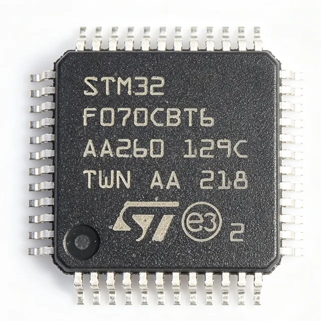
STM32F070CBT6 - ARM Cortex-M0 MCU 128KB Flash | STMicroelectronics
STM32F070CBT6

STM32F070CBT6 - ARM Cortex-M0 MCU 128KB Flash | STMicroelectronics

The STMicroelectronics STM32F070CBT6 is a 32-bit ARM Cortex-M0 microcontroller from the STM32F0 series, offering 128KB of Flash memory and 16KB of SRAM in a 48-pin LQFP package. It operates at a core frequency of up to 48 MHz and supports a supply voltage range of 2.4V to 3.6V. Data verified as of 2026-08-05. What is a microcontroller? A microcontroller (MCU) is a compact integrated circuit designed to govern a specific operation in an embedded system. It integrates a processor core, memory (Flash and SRAM), and programmable input/output peripherals on a single chip. The STM32F070CBT6 belongs to the STM32F0 series, which is part of the broader STM32 family of 32-bit ARM Cortex-M microcontrollers. This hierarchy places it within the ARM Cortex-M0 category, a low-power, entry-level core optimized for cost-sensitive applications. Key features include a 12-bit ADC with up to 16 channels, multiple communication interfaces (I2C, SPI, USART), and a variety of timers including advanced-control timers. The device also includes a DMA controller, an RTC, and a CRC calculation unit. The LQFP-48 package provides a compact footprint suitable for space-constrained designs while offering sufficient I/O pins for peripheral connectivity. The STM32F070CBT6 is built on a 32-bit ARM Cortex-M0 core with a Harvard architecture, achieving 1.25 DMIPS/MHz. It includes a nested vectored interrupt controller (NVIC) for efficient interrupt handling and supports both low-power modes (Sleep, Stop, Standby) to optimize energy consumption. The device is designed for a wide range of embedded applications requiring a balance of performance, power efficiency, and cost. Typical applications include industrial control systems, consumer electronics, IoT devices, and home automation. Its rich peripheral set and low-power capabilities make it suitable for sensor interfacing, motor control, and communication protocols. The wide operating temperature range (-40°C to +85°C) ensures reliability in harsh environments. When designing with this MCU, ensure proper decoupling of the power supply pins and consider the use of an external crystal for accurate timing. The device supports in-circuit programming and debugging via SWD, facilitating firmware development and updates. This page synthesizes distributor pricing, drop-in alternatives, and practical design notes not found in the STMicroelectronics datasheet, providing engineers with a comprehensive resource for selection and implementation.

USD $1.57 Hubungi kami
STM32F070F6P6 - 48MHz Cortex-M0 USB MCU | STMicroelectronics
STM32F070F6P6

STM32F070F6P6 - 48MHz Cortex-M0 USB MCU | STMicroelectronics

The STMicroelectronics STM32F070F6P6 is a 32-bit Arm Cortex-M0 microcontroller operating at 48 MHz, with 32 KB of Flash memory, 6 KB of SRAM, and USB support in a 20-pin TSSOP package. It is designed for compact embedded systems that need efficient control, connectivity, and peripheral integration without requiring a large pin count. A microcontroller is a programmable semiconductor device that integrates a processor core, memory, and peripherals into one package. The STM32F0 family belongs to the hierarchy of embedded processors, 32-bit microcontrollers, Arm Cortex-M devices, and power-efficient embedded control ICs. Its compact package makes the STM32F070F6P6 suitable for space-constrained products requiring a conventional GPIO-based control architecture and USB device connectivity. The principal features include an Arm Cortex-M0 processor core operating at 48 MHz, 32 KB of Flash for program storage, and 6 KB of SRAM for working memory. USB support allows the device to operate as a USB-connected peripheral in control, configuration, or data-acquisition equipment. The 20-pin TSSOP package also supports compact PCB layouts while providing sufficient I/O for common control signals. The STM32F0 architecture balances processing capability with low system complexity. Its 32-bit Arm Cortex-M0 core uses a reduced instruction set optimized for embedded control, while the 32 KB Flash region is sufficient for compact boot code, application firmware, and peripheral configuration. The 6 KB SRAM supports buffering and real-time control workloads without requiring an external memory device for modest data requirements. Typical applications include USB-enabled industrial controls, compact data-acquisition devices, PC peripheral interfaces, programmable logic controllers, instrument-control panels, and low-cost USB-to-digital or USB-to-analog interface products. The device is especially relevant when a design requires USB connectivity and a 48 MHz control loop in a small 20-pin package. PCB design should preserve the power, ground, decoupling, and signal-routing requirements specified by the manufacturer datasheet. Place the device's required decoupling capacitors close to the appropriate supply pins, route USB data as a controlled impedance differential pair, and confirm all peripheral assignments against the package pin table before releasing the layout. This product page combines the manufacturer's device information with practical engineering guidance for firmware integration, USB implementation, PCB layout, and component selection. It also provides a structured comparison with nearby STM32F0 and STM32G0 devices to support redesign and second-source decisions.

RFC Hubungi kami
STM32F071C8T6 - 48MHz Cortex-M0 64KB MCU | STMicroelectronics
STM32F071C8T6

STM32F071C8T6 - 48MHz Cortex-M0 64KB MCU | STMicroelectronics

STMicroelectronics STM32F071C8T6 is an Arm Cortex-M0 32-bit microcontroller operating up to 48 MHz, with 64 KB of embedded Flash memory, supplied in a 48-pin LQFP package. The device is positioned as a general-purpose STM32F0-series MCU for compact embedded systems requiring a 32-bit architecture, moderate Flash capacity, and a 48 MHz operating frequency. The verified distributor information identifies the STM32F071C8T6 as an STM32F0-series microcontroller with 64 KB (64K x 8) Flash and 48 MHz maximum clock speed. An STM32F0 microcontroller is an embedded microcontroller, a category within semiconductor devices that combines a processor core, memory, peripherals, and communication interfaces on one integrated circuit. The STM32F071C8T6 belongs to the STM32F071x8/xB family and uses the Arm Cortex-M0 RISC core. Its architecture is suited to control, monitoring, communication, and general-purpose embedded products where a compact 32-bit processor is useful without requiring the performance and memory of a higher-end Cortex-M series. The verified specifications emphasize three headline characteristics: a 48 MHz maximum operating frequency, 64 KB of embedded Flash memory, and a 48-pin LQFP package. The Cortex-M0 instruction set provides a straightforward 32-bit processing platform for firmware-driven products. The 64 KB Flash capacity is appropriate for firmware, configuration data, boot code, and application logic in cost-sensitive embedded designs. The LQFP-48 package provides 48 external leads and is suitable for conventional PCB assembly and inspection processes. The ST product-page description identifies the STM32F071x8/xB family as incorporating the high-performance Arm Cortex-M0 32-bit RISC core operating at up to 48 MHz. The family data also lists 12 timers, ADC, DAC, and communication interfaces, while the manufacturer datasheet result specifies a 2.0 V to 3.6 V operating range. Exact peripheral counts, pin functions, memory-map details, current consumption, and electrical limits for the exact STM32F071C8T6 ordering code should be confirmed in the manufacturer datasheet before a design is released. Typical uses include industrial control and monitoring, sensor interfaces, compact consumer products, communication modules, and low-cost embedded control boards. The 48 MHz Cortex-M0 core can handle responsive control loops and protocol servicing, while the 64 KB Flash budget supports moderate application firmware. The 48-pin LQFP package is appropriate when a design needs more external pins than a small-outline package while retaining a straightforward assembly process. The principal design consideration is power-supply and peripheral validation. The verified operating range is 2.0 V to 3.6 V, so the board supply, decoupling, I/O levels, and any communication peripherals must be selected consistently. Engineers should also check the exact pin assignment and alternate-function mapping in the ST datasheet before assigning signals, particularly for ADC, DAC, timers, and communication interfaces. This product page consolidates verified distributor pricing, manufacturer family information, package details, application guidance, and structured design notes. It is intended to help engineers and purchasers evaluate the STM32F071C8T6 efficiently while directing them to the official STMicroelectronics datasheet and product page for authoritative final validation.

RFC Hubungi kami
STM32F071CBT6 - 48MHz Cortex-M0 MCU | STMicroelectronics
STM32F071CBT6

STM32F071CBT6 - 48MHz Cortex-M0 MCU | STMicroelectronics

STMicroelectronics STM32F071CBT6 is an Arm Cortex-M0 32-bit microcontroller with a 48 MHz operating frequency, 128 KB of Flash memory, and 16 KB of SRAM in a 48-pin LQFP (7x7 mm) package. It operates from a 2.0 V to 3.6 V digital and I/O supply and integrates a 12-bit ADC, a two-channel 12-bit DAC, communication interfaces, and 12 timers for compact embedded-control designs. A microcontroller is a programmable integrated circuit that combines a processor core, memory, peripherals, and interfaces on one device. The STM32F071CBT6 belongs to the STM32F0 access-line hierarchy, where the Arm Cortex-M0 processor core sits beneath the STM32 family and the broader category of general-purpose embedded processors. Its combination of 128 KB Flash, 16 KB SRAM, and analog conversion resources supports both control logic and low-speed signal acquisition without requiring separate analog converters. The 48 MHz Cortex-M0 core provides deterministic processing for real-time control loops, while the CRC calculation unit supports data-integrity checks in communications and storage systems. The device includes seven general-purpose 16-bit timers, one 32-bit timer, and an advanced-control timer, allowing designers to allocate timer resources among periodic scheduling, input capture, output compare, motor control, or PWM generation. The integrated ADC and DAC support analog monitoring and controlled analog outputs within the same 2.0 V to 3.6 V supply domain. Communication and peripheral integration reduces the component count in embedded systems that need serial data exchange or dedicated control outputs. The verified manufacturer material identifies a CRC calculation unit, reset and power management, one 12-bit ADC, a two-channel 12-bit DAC, and multiple communication interfaces. These resources make the STM32F071CBT6 suitable for compact industrial controllers, instrumentation, consumer peripherals, and low-to-medium-speed motor-control equipment where a larger Cortex-M processor would add unnecessary cost or complexity. The 48-pin LQFP package provides a conventional surface-mount footprint with accessible leads for assembly and inspection. A 7x7 mm body preserves board area in space-constrained equipment, while the exposed thermal strategy and lead geometry support manufacturing processes that can inspect individual connections. Because this is a digital mixed-signal microcontroller rather than a discrete power semiconductor, its SOA field is not applicable. Designers should verify every peripheral assignment, alternate-function mapping, pin electrical limit, clock configuration, and decoupling requirement against the STM32F071x8/STM32F071xB manufacturer datasheet before schematic release. The 2.0 V to 3.6 V operating range and 48 MHz core frequency must be considered together when selecting external components and defining the power architecture. This page combines verified manufacturer and distributor information with a focused selection guide, package-level comparison, and application engineering notes. It also distinguishes same-package family alternatives from broader functional substitutes, helping engineers identify replacements without overlooking peripheral differences, firmware constraints, or qualification requirements.

RFC Hubungi kami