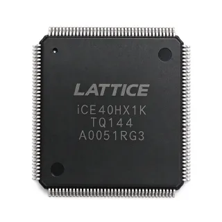
LFE2-6SE-7T144C - 6K LUT ECP2 FPGA | Lattice
MPN: LFE2-6SE-7T144C ✗ Akhir HayatLFE2-6SE-7T144C Ringkasan
An FPGA is a reconfigurable digital semiconductor that combines programmable logic blocks, programmable I/O, memory resources, and routing into one integrated circuit. The LatticeECP2 family sits within the broader programmable-logic hierarchy of FPGA, programmable-logic device, semiconductor, and embedded digital implementation. Its advantage over fixed-function logic is that interfaces, control sequences, and parallel data paths can be revised without changing the printed circuit board.
The LFE2-6SE-7T144C provides 6000 logic elements organized into 750 logic array blocks, 56320 bits of block RAM, and 90 user I/O. Its 1.14 V to 1.26 V operating supply range centers on a nominal 1.2 V rail. The SE device family includes dedicated digital signal processing resources, making it useful for parallel arithmetic, filtering, and data acquisition rather than only simple glue logic.
The -7 designation identifies the device speed grade, while 144C identifies the 144-pin commercial-temperature ordering configuration. In the TQFP package, the programmable I/O are distributed around the perimeter for board-level access. Configuration and design implementation are handled through the ECP2 development and programming environment, allowing logic, interconnections, and I/O assignments to be stored in the device configuration memory.
Typical uses include industrial automation, communications interfaces, instrumentation, embedded control, video timing, and digital signal-processing front ends. The 90 available I/O are particularly useful for parallel sensor capture, memory interfaces, control buses, and external converters. Compared with a smaller CPLD, the 6000-logic-element device supports more concurrent datapaths and embedded memory, while its 144-pin package leaves more I/O than a compact QFP device.
PCB design should preserve the device's specified core and I/O supply decoupling, confirm every bank’s voltage requirements, and route high-speed interfaces according to the LatticeECP2 layout guidance. Signal-integrity performance depends on correct termination, controlled impedance, short return paths, and separating sensitive analog or clock inputs from fast digital outputs.
This product page combines exact device characteristics with application guidance, drop-in family alternatives, and PCB-focused design notes. These engineering details help shorten component selection while making the distinction between logically similar LatticeECP2 devices explicit.
Pilihan pengganti yang segera untuk LFE2-6SE-7T144C — sama paket, pin-pin kompatibel. Bahagian paket yang berbeza memerlukan kerja ulang PCB diasingkan.
Varietas dalam siri ini
Model serupa yang kompatibel dengan pengganti yang segera LFE2-6SE-7T144C (sama faktor bentuk dan kaki) — berbeza dalam Package, Speed Grade, Core Supply Voltage, Device Type, DSP Capability.
LFE2-6E-7T144C
✅ Masuk Drop-In ⚠️ Spesifikasi Tidak DisahkanHubungi untuk harga
Lihat Datasheet →LFE2-6SE-6T144C
✅ Masuk Drop-In ⚠️ Spesifikasi Tidak DisahkanHubungi untuk harga
Lihat Datasheet →LFE2-6E-6T144C
✅ Masuk Drop-In ⚠️ Spesifikasi Tidak DisahkanHubungi untuk harga
Lihat Datasheet →LFE2-6SE-7T144I
✅ Masuk Drop-In ⚠️ Spesifikasi Tidak Disahkan📋 Alternatif rujukan (tidak dalam katalog)
LFE2-6SE-7PQ144C
✅ Masuk Drop-In ⚠️ Spesifikasi Tidak Disahkan📋 Alternatif rujukan (tidak dalam katalog)
LFE2-6SE-7T144C Penilaian maksimum & Ciri-ciri Elektrik
| FPGA Family | LatticeECP2 |
| Logic Elements | 6000 logic elements |
| Logic Array Blocks | 750 LABs |
| Embedded RAM | 56320 bits |
| User I/O | 90 I/O |
| Core Supply Voltage | 1.14 V to 1.26 V |
| Nominal Core Voltage | 1.2 V |
| Speed Grade | -7 |
| Process Technology | 90 nm |
| Kemasan | 144-pin TQFP |
| Package Dimensions | 20 mm x 20 mm |
| Terminal Type | Gull-wing surface-mount leads |
| Package Body Shape | Square |
| Digital Signal Processing | DSP resources present in the SE device family |
| Jenis Pemasangan | Surface mount |
Panduan Konfigurasi Pin LFE2-6SE-7T144C square
Konfigurasi pin untuk LFE2-6SE-7T144C (square pakai). IC digital ini termasuk GPIO, antaramuka komunikasi (UART, SPI, I2C), dan pin kuasa. Rujuk dokumen pengeluar untuk fungsi pin alternatif dan opsi konfigurasi. Biasa digunakan dalam rancangan sistem ter嵌入式 dan PCB.

Tiada data garisan pin yang diperoleh untuk LFE2-6SE-7T144C.
Rujuk kepada lembaran data untuk konfigurasi pin penuh.
Aplikasi Biasa
LFE2-6SE-7T144C patut untuk 6 aplikasis: Industrial Automation Controller, Digital Signal Processing, Communications Interface, Data Acquisition System, Instrumentation and Test Equipment, Embedded Video and Display Timing.
Industrial Automation Controller
The LFE2-6SE-7T144C fits industrial automation control because its 6000 logic elements and 90 user I/O can coordinate encoders, sensors, actuators, and operator interfaces in one programmable device. Its SE-family DSP resources can also perform scaling and filtering on sampled process data. Place the FPGA beside the field-level circuitry and use dedicated I/O for sensor inputs and actuator outputs, while the 56320 bits of embedded RAM provide local buffering. The -7 speed grade helps preserve timing margin in control paths, although the final I/O standards, timing constraints, and isolation strategy must follow the board-level safety requirements.
Disebarkan
Digital Signal Processing
The LFE2-6SE-7T144C is appropriate for digital signal processing when a design benefits from dedicated SE-family DSP blocks alongside programmable logic. Its 6000 logic elements can implement control state machines and interface logic, while the 56320 bits of embedded RAM support sample buffering and working storage. A typical signal chain can collect parallel converter outputs, perform filtering or arithmetic in the FPGA, and pass processed results to a processor or communications link. The -7 speed grade improves timing margin for pipelined operations, but designers should check DSP count, multiplier throughput, and maximum clock requirements in the LatticeECP2/M Family Data Sheet.
Disebarkan
Communications Interface
The LFE2-6SE-7T144C can serve as a communications interface controller when a product needs programmable framing, buffering, protocol conversion, and multiple parallel I/O. Its 90 user I/O support data buses and control signals to transceivers or memory devices, while 56320 bits of embedded RAM can hold packet or sample buffers. The -7 grade is useful for tightly timed word pipelines, and the SE DSP resources can support filtering or symbol-processing functions where applicable. Interface voltage standards and clock domains must be assigned to the correct power banks, with termination and impedance control implemented on the PCB.
Disebarkan
Data Acquisition System
The LFE2-6SE-7T144C is well matched to multichannel data acquisition because 90 user I/O can connect parallel converters, clocks, and acquisition control signals. The 56320 bits of embedded RAM provide local storage for samples, while the DSP resources can perform filtering, scaling, or block processing before results are transferred. The 1.14 V to 1.26 V core range must be regulated cleanly, and each I/O bank must match the voltage of the connected converter. In a high-speed acquisition board, use short data routes, controlled-impedance clocking, and separate analog and digital return paths to limit conversion and crosstalk errors.
Disebarkan
Instrumentation and Test Equipment
The LFE2-6SE-7T144C supports instrumentation designs that combine sequencing, measurement control, data formatting, and external communications. Its 6000 logic elements provide capacity for multiple instrument-state machines, while 90 I/O connect measurement front ends, relays, displays, and digital interfaces. Embedded RAM can organize acquisition records, and SE-family DSP resources can accelerate calculations on captured data. The 144-pin TQFP package offers a practical balance between I/O access and board area. For laboratory or factory equipment, validate temperature grade, supply tolerances, isolation, and calibration requirements independently of the device’s general-purpose FPGA architecture.
Disebarkan
Embedded Video and Display Timing
The LFE2-6SE-7T144C can implement video timing, pixel processing, and display-interface control when the design needs flexible logic rather than a fixed function controller. Its 90 user I/O can connect parallel pixel buses, synchronization signals, and control lines, while the programmable fabric supports test patterns, color processing, or timing compensation. The 56320 bits of embedded RAM are useful for line or small-frame buffering, and the -7 speed grade provides additional internal timing margin for wide datapaths. Panel and source interfaces still require careful voltage-bank assignment, impedance-controlled routing, and synchronization of clocks across the FPGA and display subsystem.
Disebarkan
Ringkasan Produk Disebarkan
Data referensi kejuruteraan untuk LFE2-6SE-7T144C — perbandingan, panduan rancangan, dan maklumat kesediaan
Panduan Pilihan
Perbandingan dengan Gantian
| Parametr | Produk Ini | LFE2-6E-7T144C | LFE2-6SE-6T144C | LFE2-6E-6T144C | LFE2-6SE-7T144I | LFE2-6SE-7PQ144C |
|---|---|---|---|---|---|---|
| Package | TQFP-144 | TQFP-144 | TQFP-144 | TQFP-144 | TQFP-144 | TQFP-144 |
| Brand | Lattice Semiconductor | Lattice Semiconductor | Lattice Semiconductor | Lattice Semiconductor | Lattice Semiconductor | Lattice Semiconductor |
| FPGA Family | LatticeECP2 | LatticeECP2 | LatticeECP2 | LatticeECP2 | LatticeECP2 | LatticeECP2 |
| Logic Elements | 6000 logic elements | 6000 logic elements | 6000 logic elements | 6000 logic elements | 6000 logic elements | 6000 logic elements |
| Embedded RAM | 56320 bits | 56320 bits | 56320 bits | 56320 bits | 56320 bits | 56320 bits |
| User I/O | 90 I/O | 90 I/O | 90 I/O | 90 I/O | 90 I/O | 90 I/O |
| Speed Grade | -7 | -7 | -6 | -6 | -7 | -7 |
| Core Supply Voltage | 1.14 V to 1.26 V | 1.14 V to 1.26 V | 1.14 V to 1.26 V | 1.14 V to 1.26 V | 1.14 V to 1.26 V | 1.14 V to 1.26 V |
| DSP Resources | SE-family DSP resources present | Not present | SE-family DSP resources present | Not present | SE-family DSP resources present | SE-family DSP resources present |
Penyeberangsung Jelas
- Dedicated SE-family DSP capability (vsLFE2-6E-7T144C)
- Higher -7 speed grade (vsLFE2-6SE-6T144C)
- Combines DSP, I/O density, and speed in one footprint (vsLFE2-6E-6T144C)
Catatan Desain
Plan a low-noise 1.2 V core rail for the LFE2-6SE-7T144C and assign I/O-bank supplies according to the voltage standards used by connected devices. Place the required bypass capacitors close to their corresponding power and ground pins, and keep high-current return paths away from sensitive clock and data inputs. Confirm regulator tolerance, startup behavior, and power sequencing against the LatticeECP2/M Family Data Sheet before schematic signoff.
Use the 144-pin TQFP land pattern and preserve the manufacturer's recommended pad and solder-mask geometry. Position the device so clock inputs, configuration signals, and high-speed buses have short, direct routes to their pins. Separate noisy switching returns from converter inputs and FPGA clock networks, and avoid routing fast outputs beneath or beside sensitive inputs. The package body dimensions are 20 mm by 20 mm, so courtyard clearance must account for the full TQFP footprint.
Treat clocks as dedicated routing resources and use controlled-impedance interconnects for external interfaces that exceed the FPGA's slow-edge capabilities. Match clock and data timing in the ECP2 design constraints, and use series damping or source-synchronous techniques only after signal-integrity analysis. Although the -7 grade provides internal timing margin, it does not correct PCB return-path discontinuities, crosstalk, or improperly terminated I/O.
Do not substitute a 144-pin TQFP part solely because the pin count matches. Verify the pin-description table, configuration pins, power-bank assignments, supported I/O standards, speed grade, temperature option, and SE versus E DSP resources. In particular, LFE2-6E-7T144C retains the same broad package and logic scale but does not provide the target's SE-family DSP resources, while -6 variants can alter timing closure.
Maklumat Kesediaan
The device is a programmable logic IC rather than an automotive-qualified AEC-Q100 component in this ordering configuration. RoHS, REACH, lead-free, halogen-free, and conflict-minerals declarations require confirmation from the manufacturer.