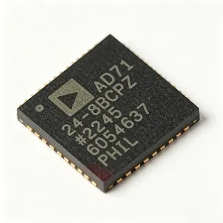
AD9652BBCZ - 16-Bit 310 MSPS Dual ADC | Analog Devices
MPN: AD9652BBCZ ✓ Active| Qty | Unit Price | Extended |
|---|---|---|
| 1 | $89.5 | $89.50 |
| 10 | $82.3 | $823.00 |
| 100 | $74.1 | $7,410.00 |
| 500 | $66.8 | $33,400.00 |
| 1,000 | $60.2 | $60,200.00 |
AD9652BBCZ Overview
An ADC (Analog-to-Digital Converter) is a critical component in signal processing chains that converts continuous analog signals into discrete digital values for processing by digital systems. The AD9652 is a pipelined ADC, a type of ADC architecture that uses multiple stages to achieve high speed and high resolution simultaneously. Pipelined ADCs are widely used in applications such as communications, radar, and medical imaging, where high sample rates and high resolution are essential. The AD9652 fits into the broader category of data converters, which are fundamental building blocks in mixed-signal systems.
Key features of the AD9652 include dual 16-bit ADCs with sampling rates up to 310 MSPS, a 3-wire SPI-compatible serial interface for programming and control, and LVDS output data with a double data rate (DDR) clock. The device also includes an overrange bit for each ADC, providing additional dynamic range information. The AD9652 is specified over the industrial temperature range of -40°C to +85°C, ensuring reliable operation in demanding environments.
The AD9652 utilizes a pipelined architecture that balances speed and resolution, achieving high dynamic performance while maintaining low power consumption. The device integrates two ADCs in a single package, reducing board space and simplifying system design. The LVDS outputs support high-speed data transfer with minimal noise, and the SPI interface allows flexible configuration of the device's operating modes.
Typical applications for the AD9652 include communications systems (such as base stations and software-defined radios), radar systems, medical imaging equipment, and test and measurement instruments. Its high sample rate and resolution make it ideal for capturing wideband signals with high fidelity.
When designing with the AD9652, it is important to provide clean power supplies and proper decoupling to achieve optimal performance. The device's LVDS outputs should be terminated correctly to ensure signal integrity at high data rates.
Drop-in alternatives for AD9652BBCZ — same package, pin-to-pin compatible. Different-package parts requiring PCB rework are excluded.
Variants in this series
Same-series models that are drop-in compatible with AD9652BBCZ (same form factor and footprint) — differing in Package, Sampling Rate, Supply Voltage, Data Interface, Number of Inputs.
Quick Comparison Tool — Select alternative parts for side-by-side comparison:
AD9652BBCZ-310
✅ Drop-In📋 Reference alternative (not in catalog)
AD9652BBCZ-310
✅ Drop-In📋 Reference alternative (not in catalog)
AD9652BBCZ-310
✅ Drop-In📋 Reference alternative (not in catalog)
AD9652BBCZ-310
✅ Drop-In📋 Reference alternative (not in catalog)
AD9652BBCZ-310
✅ Drop-In📋 Reference alternative (not in catalog)
AD9652BBCZ-310
✅ Drop-In📋 Reference alternative (not in catalog)
AD9652BBCZ-310
✅ Drop-In📋 Reference alternative (not in catalog)
AD9652BBCZ-310
✅ Drop-In📋 Reference alternative (not in catalog)
AD9652BBCZ Maximum Ratings & Electrical Characteristics
| Resolution | 16 bit |
| Sampling Rate | 310 MSPS |
| Number of Inputs | 2 |
| Input Type | Differential |
| Data Interface | LVDS |
| Architecture | Pipelined |
| Supply Voltage | 3.3 V / 1.8 V |
| Package | 144-CSPBGA (10x10 mm) |
| Operating Temperature Range | -40°C to +85°C |
| Input Frequency Range | Up to 465 MHz |
| Output Data Format | LVDS with DDR clock |
| Serial Interface | 3-wire SPI |
| Overrange Bit | Yes |
| Mounting Type | Surface Mount |
| RoHS Status | Compliant |
AD9652BBCZ Pin Configuration
| Pin A1 | AVDD — Analog power supply (3.3 V) |
| Pin A2 | VIN+ — Positive differential analog input |
| Pin A3 | VIN- — Negative differential analog input |
| Pin B1 | AVSS — Analog ground |
| Pin B2 | VREF — Voltage reference input/output |
| Pin C1 | CLK+ — Positive differential clock input |
| Pin C2 | CLK- — Negative differential clock input |
| Pin D1 | DVDD — Digital power supply (1.8 V) |
| Pin D2 | DVSS — Digital ground |
| Pin E1 | SCLK — SPI serial clock |
| Pin E2 | SDIO — SPI serial data I/O |
| Pin F1 | CSB — SPI chip select (active low) |
| Pin G1 | D0P — LVDS data output positive (bit 0) |
| Pin G2 | D0N — LVDS data output negative (bit 0) |
| Pin H1 | DCLKP — LVDS data clock positive |
| Pin H2 | DCLKN — LVDS data clock negative |
Typical Applications
AD9652BBCZ is suitable for 6 applications: Communications Systems, Radar Systems, Medical Imaging, Test and Measurement, Communications Infrastructure, Electronic Warfare.
Communications Systems
The AD9652BBCZ is ideal for communications systems such as base stations and software-defined radios. Its 310 MSPS sampling rate and 16-bit resolution enable direct digitization of wideband signals, simplifying receiver architectures. The high input bandwidth up to 465 MHz allows capturing multiple channels simultaneously, improving spectral efficiency. The dual ADC configuration supports diversity reception, enhancing link reliability. The LVDS outputs with DDR clock ensure high-speed data transfer with minimal signal integrity issues, critical for maintaining signal quality in dense digital environments.
Recommended
Radar Systems
In radar systems, the AD9652BBCZ provides high-speed digitization of IF signals with 16-bit resolution, enabling accurate target detection and ranging. Its 310 MSPS sampling rate supports wideband waveforms, improving range resolution. The dual ADC channels allow simultaneous I/Q sampling, essential for coherent processing. The wide input frequency range up to 465 MHz enables direct IF sampling, reducing analog front-end complexity. The industrial temperature range ensures reliable operation in harsh environments, making it suitable for defense and aerospace applications.
Recommended
Medical Imaging
The AD9652BBCZ is well-suited for medical imaging applications such as ultrasound and MRI. Its high resolution and sampling rate enable precise digitization of analog signals, improving image quality. The dual ADC configuration supports multi-channel acquisition, essential for array transducers. The low noise performance and wide dynamic range help detect subtle differences in tissue density. The compact 144-ball CSP_BGA package allows integration into space-constrained imaging systems, while the SPI interface simplifies configuration for different imaging modes.
Recommended
Test and Measurement
In test and measurement equipment, the AD9652BBCZ provides high-speed, high-resolution digitization for oscilloscopes, spectrum analyzers, and data acquisition systems. Its 310 MSPS sampling rate captures fast transients with high fidelity, while 16-bit resolution ensures accurate amplitude measurements. The dual channels enable simultaneous acquisition of multiple signals, useful for differential measurements. The LVDS outputs support high-speed data streaming to FPGAs or DSPs, enabling real-time analysis. The wide input bandwidth allows direct measurement of RF signals without downconversion.
Recommended
Communications Infrastructure
The AD9652BBCZ is used in communications infrastructure such as microwave backhaul and satellite ground stations. Its high sampling rate and resolution enable efficient digitization of wideband signals, supporting high data rates. The dual ADC configuration allows for diversity reception and MIMO applications. The device's low power consumption and small package make it suitable for dense PCB layouts. The SPI interface allows dynamic reconfiguration for different standards, enhancing flexibility in multi-standard base stations.
Recommended
Electronic Warfare
In electronic warfare systems, the AD9652BBCZ provides high-speed digitization of wideband signals for signal intelligence and jamming. Its 310 MSPS sampling rate and 16-bit resolution enable detection of weak signals in dense electromagnetic environments. The wide input bandwidth up to 465 MHz allows monitoring of multiple frequency bands simultaneously. The dual ADC channels support direction-finding applications. The rugged industrial temperature range and high reliability make it suitable for military platforms.
Recommended
Recommended Products Summary
Engineering reference data for AD9652BBCZ — comparison, design guidance, and compliance information.
Selection Guide
Comparison with Alternatives
| Parameter | This Product | AD9652BBCZ-310 |
|---|---|---|
| Package | 144-CSPBGA (10x10 mm) | 144-CSPBGA (10x10 mm) |
| Brand | Analog Devices | Analog Devices |
| Resolution | 16 bit | 16 bit |
| Sampling Rate | 310 MSPS | 310 MSPS |
| Number of Inputs | 2 | 2 |
| Data Interface | LVDS | LVDS |
| Supply Voltage | 3.3 V / 1.8 V | 3.3 V / 1.8 V |
| Operating Temperature | -40°C to +85°C | -40°C to +85°C |
Key Differentiators
- Dual 16-bit ADC with 310 MSPS sampling rate (vs AD9652BBCZ-310)
- Wide input bandwidth up to 465 MHz (vs AD9652BBCZ-310)
- LVDS outputs with DDR clock (vs AD9652BBCZ-310)
Design Notes
Provide clean power supplies for AVDD (3.3 V) and DVDD (1.8 V). Use low-dropout regulators (LDOs) with low noise and high PSRR to minimize supply-induced noise. Place 0.1 uF and 10 uF decoupling capacitors close to each power pin. Consider using ferrite beads to isolate analog and digital supplies.
For optimal performance, use a multi-layer PCB with dedicated ground planes for analog and digital sections. Route differential input traces with controlled impedance (e.g., 100 ohms) and keep them as short as possible. Ensure the clock input is clean and has low jitter, as it directly affects SNR. Use series termination resistors on LVDS outputs to match transmission line impedance.
Avoid routing digital output traces near analog inputs to prevent coupling. Ensure the SPI interface is properly configured before starting conversions. Do not exceed the absolute maximum ratings for supply voltages. Provide adequate thermal relief for the CSP_BGA package to prevent overheating. Verify that the input signal is within the common-mode range to avoid clipping.
Compliance Information
RoHS compliance is indicated by the 'Z' suffix in the part number. Other compliance details are not explicitly stated in the provided data.