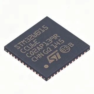
CLRC66303HN - 13.56MHz Multi-Protocol NFC Frontend | NXP
MPN: CLRC66303HN ✓ Active| Qty | Unit Price | Extended |
|---|---|---|
| 1 | $2.52 | $2.52 |
| 10 | $2.39 | $23.90 |
| 100 | $2.14 | $214.00 |
| 500 | $1.94 | $970.00 |
| 1,000 | $1.77 | $1,770.00 |
CLRC66303HN Overview
An NFC frontend is the analog radio layer of a contactless system: it sits between a host microcontroller and the antenna coil, generating the 13.56 MHz carrier, modulating and demodulating signals, and handling framing at the physical layer. In the system hierarchy it belongs to the family of RFID reader ICs, contactless transceiver ICs, and wireless connectivity semiconductors. The host MCU only needs to interpret protocol frames over SPI, I2C, or serial UART, dramatically reducing firmware complexity.
Key features of the CLRC663 plus family include highly flexible multi-protocol support in a single device, a highly efficient integrated analog front end, programmable transmitter output power, and low-power operating modes suited to battery-powered access control terminals. DigiKey classifies the part as an RFID Reader/Transponder IC supporting ISO 14443 with I2C, SPI and UART host interfaces at 2.5V to 5.5V in a 32-VFQFN exposed-pad package.
Technically, the device integrates the complete analog front end: low-jitter quartz-stabilized 13.56 MHz carrier generation, programmable TX driver stages, low-noise RX path with programmable gain, automatic antenna tuning assistance, and extensive digital register-level configurability through the host interface. The 32-VFQFN exposed pad provides good RF ground return and thermal performance for compact reader designs.
Typical applications include access control readers, gaming and lottery terminals, industrial RFID readers, and NFC-capable point-of-sale or handheld devices, all cited by NXP as target use cases for the CLRC663 plus family.
Design consideration: antenna matching is the most critical aspect of a CLRC663 design - follow the NXP antenna design application note and use the 50-ohm or direct-matching network per datasheet guidance; verify EMC compliance on the first layout revision.
This page adds value beyond the datasheet by synthesizing distributor pricing, drop-in family alternatives, comparison tables, and practical design notes in one place.
Drop-in alternatives for CLRC66303HN — same package, pin-to-pin compatible. Different-package parts requiring PCB rework are excluded.
Quick Comparison Tool — Select alternative parts for side-by-side comparison:
CLRC66301HN
✅ Drop-In ⚠️ 参数待验证📋 Reference alternative (not in catalog)
CLRC66302HN
✅ Drop-In ⚠️ 参数待验证📋 Reference alternative (not in catalog)
CLRC66303HNY
✅ Drop-In📋 Reference alternative (not in catalog)
MFRC63002HN
✅ Drop-In ⚠️ 参数待验证📋 Reference alternative (not in catalog)
MFRC63102HN
✅ Drop-In ⚠️ 参数待验证📋 Reference alternative (not in catalog)
CLRC66303HN Specifications
| Product Type | Multi-protocol NFC frontend / RFID reader IC |
| Carrier Frequency | 13.56 MHz |
| Supply Voltage Range | 2.5 V to 5.5 V |
| Supported Protocols | ISO/IEC 14443A (MIFARE), ISO/IEC 14443B, ISO/IEC 15693, ISO/IEC 18000-3 mode 3, FeliCa |
| Host Interfaces | SPI, I2C, UART |
| Package | 32-VFQFN exposed pad (HVQFN-32) |
| Mounting Type | Surface Mount |
| Application Domains | Access control, gaming, industrial |
| Operation Mode | Reader / Writer (PCD / VCD) |
| Antenna Output | Integrated TX driver stages |
| Receiver | Integrated low-noise RX path, programmable gain |
| Family | CLRC663 plus |
| Lifecycle Status | Active (per NXP product page) |
CLRC66303HN 32-vfqfn exposed pad (hvqfn-32) Pin Configuration Guide
Pin configuration for CLRC66303HN (32-vfqfn exposed pad (hvqfn-32) package). Pin numbering, functions, and connection diagrams are defined in the manufacturer datasheet. Refer to it for the exact footprint and soldering guidelines.

No detailed pinout data available for CLRC66303HN.
Refer to the datasheet for full pin configuration.
Typical Applications
CLRC66303HN is suitable for 6 applications: Access Control Readers, Gaming and Lottery Terminals, Industrial RFID Readers, Handheld and Portable NFC Devices, Point-of-Sale and Payment Terminals, Embedded Tag Writer Stations.
Access Control Readers
The CLRC66303HN is one of NXP's primary recommendations for access control, where buildings and campuses mix MIFARE Classic, MIFARE DESFire, and legacy 15693 credentials. Supporting ISO 14443A/B and ISO 15693 simultaneously in one silicon lets a single reader product cover an entire installed credential base without multiple SKUs. The 2.5V to 5.5V supply range accepts standard PoE-derived or battery-backed rails, and the SPI host interface delivers the low card-processing latency needed for fast door-open response. Designers should implement alternating-protocol polling and use the exposed-pad VFQFN thermal/ground path for a stable RF reference in wall-mounted enclosures.
Recommended
Gaming and Lottery Terminals
NXP explicitly lists gaming as a CLRC663 plus target market, where FeliCa and ISO 14443 support is used for player cards, chip authentication, and stored-value wallets. The CLRC66303HN's multi-protocol frontend lets a gaming terminal read customer cards across regional standards (FeliCa in Japan, MIFARE elsewhere) with one PCB. Register-level control of TX power and receive gain lets engineers optimize read range for both short-range secure taps and longer-range card presentation zones. Its 13.56 MHz field is generated from a quartz-stabilized oscillator, meeting the timing accuracy that gaming regulators typically require for transactional card interfaces.
Recommended
Industrial RFID Readers
For industrial use cases such as tool identification, asset tracking, and production-line kitting, the CLRC66303HN reads ISO 15693 and ISO 18000-3 mode 3 tags that offer larger memory and longer range than 14443 cards. Its wide 2.5V to 5.5V input tolerates noisy industrial power rails when combined with local regulation, and the UART interface simplifies integration into PLC-adjacent modules and retrofit reader boxes. The exposed-pad HVQFN-32 withstands vibration better than leaded packages when properly soldered. Engineers should derate read range expectations around metal fixtures and apply ferrite shielding on the antenna per NXP's industrial reference designs.
Recommended
Handheld and Portable NFC Devices
Battery-powered handheld readers benefit from the CLRC663 plus family's low-power modes and its 2.5V minimum supply, which allows direct operation from a Li-ion cell via a small LDO. The SPI interface supports fast wakeup and polling cycles managed by the host MCU, so the frontend can stay in standby between reads and cut average current dramatically versus always-on polling. Typical products include inventory scanners, maintenance diagnostic tools, and portable ticket validators. Designers should sequence the antenna TX power through software to limit peak battery load and use the VFQFN exposed pad as a compact thermal and RF ground return.
Recommended
Point-of-Sale and Payment Terminals
The CLRC66303HN serves payment and vending terminals that must read MIFARE-based transit cards, campus wallets, and NFC forum tags. Its simultaneous 14443A/14443B coverage and FeliCa support address the regional diversity of closed-loop payment cards, while the SPI interface keeps transaction latency low at the checkout. The quartz-stabilized 13.56 MHz carrier and NXP's long RF design heritage support the timing precision expected in payment acceptance. Because payment terminals face EMC and radio regulatory testing, follow the matching network values in NXP's reference design exactly on the first layout to minimize requalification cycles.
Recommended
Embedded Tag Writer Stations
Production and personalization stations that program NTAG, MIFARE, and ICODE tags benefit from the CLRC66303HN's write support across 14443A and 15693 families in one device. A single fixture hardware design can serialize different tag types on the same line, controlled purely by firmware protocol selection. The UART interface integrates easily with PC-hosted encoding software through a USB-serial bridge, and the register-level configurability lets the station tune RF parameters per tag type for reliable write margins. In factory use, verify antenna matching with each fixture coil batch, since inductance spread directly affects write reliability at the edge of the field.
Recommended
Recommended Products Summary
Engineering reference data for CLRC66303HN — comparison, design guidance, and compliance information.
Selection Guide
Comparison with Alternatives
| Parameter | This Product | CLRC66301HN | CLRC66302HN | CLRC66303HNY | MFRC63002HN | MFRC63102HN |
|---|---|---|---|---|---|---|
| Package | 32-VFQFN exposed pad | 32-VFQFN exposed pad - same | 32-VFQFN exposed pad - same | 32-VFQFN exposed pad - same | 32-VFQFN exposed pad - same | 32-VFQFN exposed pad - same |
| Brand | NXP Semiconductors | NXP Semiconductors | NXP Semiconductors | NXP Semiconductors | NXP Semiconductors | NXP Semiconductors |
| Carrier Frequency | 13.56 MHz | 13.56 MHz | 13.56 MHz | 13.56 MHz | 13.56 MHz | 13.56 MHz |
| Supply Voltage | 2.5 V to 5.5 V | 2.5 V to 5.5 V | 2.5 V to 5.5 V | 2.5 V to 5.5 V | 2.5 V to 5.5 V | 2.5 V to 5.5 V |
| Host Interfaces | SPI, I2C, UART | SPI, I2C, UART | SPI, I2C, UART | SPI, I2C, UART | SPI, I2C, UART | SPI, I2C, UART |
| Protocol Coverage | 14443A/MIFARE, 14443B, 15693, 18000-3 m3, FeliCa | Reduced subset of CLRC663 protocols | Reduced subset of CLRC663 protocols | Same as CLRC66303HN | 14443A/MIFARE only | 14443A + 14443B |
| Lifecycle Status | Active | Active | Active | Active (ships today per DigiKey) | Active | Active |
Key Differentiators
- Broadest protocol coverage in the NXP 13.56 MHz reader family (vs MFRC63002HN)
- Full multi-protocol support at lower cost than the PN5180 platform (vs PN5180)
- Identical drop-in silicon availability via HNY ordering variant (vs CLRC66303HNY)
Design Notes
The antenna matching network is the single most critical part of a CLRC66303HN design. Follow the NXP CLRC663 antenna design application note: measure the actual coil inductance of each PCB batch, compute the series/parallel matching capacitors for the target Q factor, and place the network within a few millimeters of the TX pins. Use the exposed pad of the HVQFN-32 as a solid RF ground - connect it to the ground plane with an array of vias. Follow NXP's reference design component values on the first layout to minimize EMC retest risk.
The CLRC66303HN operates from 2.5V to 5.5V, but RF output power and receiver sensitivity depend on supply quality. Decouple the supply pins with a combination of bulk capacitance (10uF) and high-frequency ceramics (100nF close to each supply pin). If the rail comes from a switching converter, add an LC filter or an LDO stage before the CLRC663, since switching ripple couples into the 13.56 MHz RX path and reduces read range. Estimated power budget: total transmit-phase current must be taken from the datasheet electrical characteristics table for your selected TX gain setting.
Do not assume all CLRC663 plus ordering codes are functionally identical - the 66301/66302/66303 variants differ in the protocol and feature subsets enabled in silicon, so a BOM substitution within the family must be verified against the NXP ordering information table and your required protocol list. Also confirm the interface mode strapping pins on power-up: incorrect strapping leaves the device on the wrong host interface and the MCU sees no response, which is frequently misdiagnosed as a hardware fault rather than a configuration issue.
Compliance Information
NXP product page includes an Environmental Quality section; exact RoHS/REACH status must be confirmed from the NXP product page or certificate of conformance. NXP standard commercial parts are typically RoHS compliant, but this must not be assumed without data.