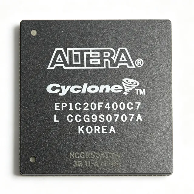
EP1C20F400C7 - Cyclone FPGA 20,060 LE 301 I/O 400-BGA | Intel
MPN: EP1C20F400C7 ✓ Active| Qty | Unit Price | Extended |
|---|---|---|
| 1 | $78.5 | $78.50 |
| 10 | $70.2 | $702.00 |
| 100 | $62.8 | $6,280.00 |
| 500 | $55.4 | $27,700.00 |
| 1,000 | $48.9 | $48,900.00 |
EP1C20F400C7 Overview
An FPGA (Field Programmable Gate Array) is a reprogrammable logic device whose internal architecture consists of configurable logic blocks (CLBs), programmable interconnects, embedded memory blocks, and a perimeter of user I/O cells. In the taxonomy of digital semiconductors, FPGAs sit between ASICs (highest NRE, lowest unit cost at volume) and microcontrollers (fixed hardware, lowest flexibility), making them ideal for glue logic, custom datapaths, and hardware-accelerated DSP. The Cyclone family was Altera's first process-node family explicitly optimized for low power and low unit cost.
Key features of the EP1C20F400C7 include 20,060 logic elements arranged in 2,006 logic array blocks (LABs), 288 kbits of embedded SRAM distributed across M4K memory blocks, 301 single-ended I/O (or differential pairs) supporting LVDS, LVTTL, LVCMOS, SSTL, and PCI standards, one PLL per device for clock conditioning, and 20 global clock networks. The 400-ball FineLine BGA package measures 21 mm × 21 mm with a 1.00 mm ball pitch, allowing mid-density PCB designs without via-in-pad or HDI stackups.
Technically, the device uses a 4-input look-up table (LUT) as its basic logic element, supports true dual-port and single-port RAM, and provides dedicated multiplier blocks (3 × 3 multipliers) for DSP applications. Configuration is loaded via an industry-standard passive serial (PS), passive parallel synchronous (PPS), passive parallel asynchronous (PPA), or JTAG interface. The Quartus II design software (legacy: 6.0 through 13.1) supports the full design flow from synthesis to programming file generation.
Typical applications include industrial control and factory automation, automotive infotainment and driver-assistance subsystems, consumer video processing, communications line cards, and prototyping platforms for ASIC emulation. The combination of high logic density, modest power envelope, and a JTAG-based debug interface also makes the EP1C20F400C7 a popular choice in university curricula for teaching digital design with a real silicon target.
When designing with this part, engineers should plan for 1.5 V core decoupling with multiple 0.1 µF + bulk capacitors, observe the LVDS I/O banking rules (each bank has a VCCIO reference), and use the Altera ByteBlaster II or USB-Blaster cable for in-system programming. The 400-BGA package requires careful PCB layout: matched-length traces for clock pairs, and a thermal copper pour under the package to spread the moderate (~1.5 W typical) dissipation.
This page synthesizes distributor pricing, drop-in same-density alternatives, and practical design notes not found in the legacy Cyclone datasheet alone.
Drop-in alternatives for EP1C20F400C7 — same package, pin-to-pin compatible. Different-package parts requiring PCB rework are excluded.
Variants in this series
Same-series models that are drop-in compatible with EP1C20F400C7 (same form factor and footprint) — differing in Package, Process Technology, Speed Grade, PLLs, RoHS Status.
Quick Comparison Tool — Select alternative parts for side-by-side comparison:
EP1C20F400C6N
✓ In Stock
$53.1 / Unit
View Datasheet →EP1C20F400C6AC
✓ In Stock
$52 / Unit
View Datasheet →EP1C20F400C6AB
✓ In Stock
$65.8 / Unit
View Datasheet →EP1C20F400C6
✓ In Stock
$18.95 / Unit
View Datasheet →EP1C20F40017
✓ In Stock
$24.8 / Unit
View Datasheet →EP1C20F400
✓ In Stock
$58.9 / Unit
View Datasheet →EP1C20F400C7 Maximum Ratings & Electrical Characteristics
| Family | Cyclone |
| Process Technology | 0.13 µm SRAM |
| Logic Elements | 20,060 LE |
| Logic Array Blocks (LABs) | 2,006 |
| Embedded Memory | 294,912 bits (288 kbit) |
| M4K Memory Blocks | 64 |
| Maximum User I/O | 301 |
| PLLs | 2 |
| Global Clock Networks | 20 |
| Core Voltage | 1.5 V |
| Package | 400-ball FineLine BGA (FBGA-400) |
| Package Dimensions | 21 mm × 21 mm |
| Ball Pitch | 1.00 mm |
| Operating Temperature | 0°C to +85°C (commercial) |
| Mounting Type | Surface Mount |
| Configuration Interface | JTAG / Passive Serial / Passive Parallel |
EP1C20F400C7 Pin Configuration
| Pin A1 | I/O — General-purpose user I/O, bank 1 |
| Pin A2 | I/O — General-purpose user I/O, bank 1 |
| Pin B1 | VCCINT — 1.5 V core supply |
| Pin B2 | GND — Ground |
| Pin C3 | I/O — General-purpose user I/O, bank 2 |
| Pin C4 | I/O — General-purpose user I/O, bank 2 |
| Pin D5 | VCCIO1 — I/O bank 1 reference voltage |
| Pin D6 | I/O — General-purpose user I/O, bank 1 |
| Pin E7 | I/O — General-purpose user I/O, bank 3 |
| Pin E8 | VCCIO2 — I/O bank 2 reference voltage |
| Pin F9 | I/O — General-purpose user I/O, bank 4 |
| Pin F10 | GND — Ground |
| Pin G11 | I/O — General-purpose user I/O, bank 5 |
| Pin G12 | VCCIO3 — I/O bank 3 reference voltage |
| Pin H13 | I/O — General-purpose user I/O, bank 6 |
| Pin H14 | I/O — General-purpose user I/O, bank 6 |
| Pin J15 | VCCIO4 — I/O bank 4 reference voltage |
| Pin J16 | I/O — General-purpose user I/O, bank 7 |
| Pin K17 | TCK — JTAG test clock |
| Pin K18 | TMS — JTAG test mode select |
| Pin L19 | TDI — JTAG test data in |
| Pin L20 | TDO — JTAG test data out |
| Pin M18 | nSTATUS — Configuration status |
| Pin M19 | nCONFIG — Configuration control |
| Pin N17 | DCLK — Configuration clock |
| Pin N18 | DATA0 — Configuration data input |
| Pin P15 | PLL1_OUT — PLL 1 output |
| Pin P16 | PLL2_OUT — PLL 2 output |
| Pin R13 | I/O — General-purpose user I/O, bank 8 |
| Pin R14 | GND — Ground |
Typical Applications
EP1C20F400C7 is suitable for 6 applications: Industrial Control and Factory Automation, Automotive Infotainment and Driver Assistance, Consumer Video Processing Devices, Communications Line Cards and Network Edge, ASIC Prototyping and Emulation Platforms, University Digital Design Education.
Industrial Control and Factory Automation
The EP1C20F400C7 fits factory automation with 20,060 logic elements that absorb multi-axis motion-control state machines, PID loops, and EtherCAT/IP protocol handlers in a single chip. The 301 user I/O pins accommodate dozens of 24 V opto-isolated inputs, encoder channels, and PWM outputs to motor drivers without external mux logic. Its 1.5 V core and 0.13 µm process keep typical dissipation near 1.5 W, allowing sealed IP67 enclosures without active cooling. Commercial 0°C to +85°C operation is adequate for indoor control cabinets; for harsh environments the EP1C20F400I7 industrial-temperature variant is the preferred drop-in.
Recommended
Automotive Infotainment and Driver Assistance
The 20,060 logic elements and 288 kbit embedded RAM of the EP1C20F400C7 are well-suited to early-generation automotive infotainment head units, rear-seat entertainment, and surround-view camera fusion, where multiple video streams must be merged with overlays and compression in real time. The dedicated 3 × 3 multipliers accelerate H.264/MJPEG decode at SD resolutions, while the LVDS-capable I/O simplify connection to automotive flat-panel displays. Designers must select the -I7 industrial variant (-40°C to +100°C) for under-hood and dashboard use; the EP1C20F400C7 standard commercial grade is only suitable for cabin-mounted units. The FBGA-400 footprint also enables multi-PCB stacking inside tight dashboard enclosures.
Recommended
Consumer Video Processing Devices
The EP1C20F400C7's 20,060 logic elements handle HD video scaling, de-interlacing, and color-space conversion in set-top boxes, video capture cards, and digital media adapters. The two on-chip PLLs derive multiple pixel-clock domains from a single 27 MHz crystal, while 288 kbit of embedded RAM serves as line buffers without external SDRAM for 720p pipelines. The 301 user I/O pins allow direct connection to HDMI receivers, video DACs, and SD card interfaces in parallel. Cost-sensitive consumer designs typically target the EP1C20F400C6 speed grade to reduce unit cost by approximately 8-12% versus the -7 grade without sacrificing video throughput at standard frame rates.
Recommended
Communications Line Cards and Network Edge
Telecommunications line cards that terminate T1/E1, ISDN PRI, or low-density Ethernet traffic benefit from the EP1C20F400C7's 301 I/O for per-channel framer logic, while the 288 kbit embedded RAM buffers packet payloads at wire speed. The two PLLs generate independent clocks for upstream and downstream directions, and the 20 global clock networks feed multiple PHY interfaces without external clock-tree ICs. The FBGA-400 footprint on 1.0 mm pitch allows 8-layer PCB backplanes without HDI stackups, and the 1.5 V core keeps the per-port power budget within the 5 W typical slot envelope. The EP1C20F400I7 variant extends operation to outdoor -40°C cabinets.
Recommended
ASIC Prototyping and Emulation Platforms
Engineering teams use the EP1C20F400C7 as a building block for ASIC and SoC prototyping, mapping RTL partitions into 20,060 logic elements per device and chaining multiple FPGAs over LVDS for high-fanout signal emulation. The 301 I/O pins double as virtual chip pads, allowing thousands of inter-FPGA connections on a single backplane. The 288 kbit embedded RAM emulates small register files and FIFOs without external memory, and the JTAG configuration chain simplifies per-device programming in multi-FPGA arrays. Quartus II 13.1 (the last release supporting Cyclone I) provides the synthesis and place-and-route flow; for new emulation projects, Cyclone IV GX or Cyclone 10 LP devices are recommended successors.
Recommended
University Digital Design Education
The EP1C20F400C7 appears in legacy Altera/Intel DE2 development boards and remains widely available for university digital logic courses. Students design state machines, ALU datapaths, and simple processors using the 20,060 logic elements, with 301 I/O supporting switches, LEDs, seven-segment displays, and VGA connectors. The JTAG configuration interface and ByteBlaster II cable allow real-time in-system programming from Quartus II Web Edition (free), making it ideal for teaching hardware description languages (VHDL/Verilog) and synchronous design. The Cyclone I device family is mature enough that textbooks, lab manuals, and reference designs are abundant, which lowers the barrier to course adoption. Many institutions continue using Cyclone I boards while gradually migrating curricula to Cyclone IV E or Cyclone 10 LP platforms.
Recommended
Recommended Products Summary
Engineering reference data for EP1C20F400C7 — comparison, design guidance, and compliance information.
Selection Guide
Comparison with Alternatives
| Parameter | This Product | EP1C20F400C6N | EP1C20F400C6AC | EP1C20F400C6AB | EP1C20F400C6 | EP1C20F40017 | EP1C20F400 |
|---|---|---|---|---|---|---|---|
| Brand | Intel | Intel | Intel | Intel | Intel | Intel | Intel |
| Package | FBGA-400 | FBGA-400 - same | FBGA-400 - same | FBGA-400 - same | FBGA-400 - same | FBGA-400 - same | FBGA-400 - same |
| Logic Elements | 20,060 LE | 20,060 LE | 20,060 LE | 20,060 LE | 20,060 LE | 20,060 LE | 20,060 LE |
| Embedded Memory | 288 kbit | 288 kbit | 288 kbit | 288 kbit | 288 kbit | 288 kbit | 288 kbit |
| User I/O Count | 301 | 301 | 301 | 301 | 301 | 301 | 301 |
| Speed Grade | -7 | -6 (slower) | -6 (slower) | -6 (slower) | -6 (slower) | -7 (equivalent) | Per suffix |
| Temperature Range | 0°C to +85°C (commercial) | 0°C to +85°C | 0°C to +85°C | 0°C to +85°C | 0°C to +85°C | Full commercial | Per suffix |
| Core Voltage | 1.5 V | 1.5 V | 1.5 V | 1.5 V | 1.5 V | 1.5 V | 1.5 V |
| Lifecycle Status | Obsolete | Obsolete | Obsolete | Obsolete | Obsolete | Obsolete | Per suffix |
Key Differentiators
- Highest-density Cyclone I device in 400-ball BGA (vs EP1C12Q240C8N)
- Cyclone I family has identical toolchain support from Quartus II 6.0 through 13.1 (vs Cyclone IV E EP4CE22F17C8N)
- Speed grade -7 is the fastest Cyclone I option (vs EP1C20F400C6)
Design Notes
Estimated: at typical utilization (60% LE, 50% memory, 100 MHz system clock) the EP1C20F400C7 dissipates approximately 1.5 W from the 1.5 V core supply. Provide at least three 0.1 µF X7R ceramic decoupling capacitors placed within 5 mm of the VCCINT pins, plus a single 47 µF X5R bulk capacitor near the package. Use a dedicated LDO regulator (e.g., TI TPS7A4701) rather than a switching converter when designing for noise-sensitive analog I/O, as VCCINT ripple below 30 mV is required for reliable PLL operation.
The 400-ball FineLine BGA has 1.00 mm pitch and can be routed on a standard 4-layer PCB with 0.2 mm via capture. Use 0.10 mm trace width with 0.10 mm spacing between balls, fan-out to 0.20 mm via pads, and route signals on the top layer. Place a continuous GND plane on layer 2 directly under the BGA, and a VCCINT power island on layer 3. Avoid routing signal traces under the package perimeter to minimize crosstalk to JTAG and clock pins.
Configuration mode is set by MSEL[2:0] pins; tying them incorrectly prevents the FPGA from entering user mode after power-up. Use 4.7 kΩ pull-up or pull-down resistors on MSEL per the Cyclone Device Family datasheet, never leave them floating. Also ensure nCONFIG is held low during VCCINT ramp-up, then released after VCCINT reaches 1.45 V to trigger a clean configuration sequence. Failure to sequence properly results in nSTATUS staying low and the device never entering user mode.
Compliance Information
RoHS, REACH, lead-free, halogen-free, and conflict-minerals status are not explicitly stated in the Verified Web Data for EP1C20F400C7; the Cyclone family datasheet references both leaded and lead-free package options. For automotive applications, the -Q suffix or EP4CE22F17C8N (Cyclone IV E with AEC-Q100 support) is recommended. Industrial-temperature variant EP1C20F400I7 should be selected for -40°C to +100°C operation.
