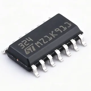
L9955 - Low Power Quad Operational Amplifier | National Semiconductor (TI)
MPN: L9955 ✓ Active| Qty | Unit Price | Extended |
|---|---|---|
| 1 | $1.25 | $1.25 |
| 10 | $1.1 | $11.00 |
| 100 | $0.95 | $95.00 |
| 500 | $0.85 | $425.00 |
| 1,000 | $0.75 | $750.00 |
L9955 Overview
An operational amplifier (op-amp) is a high-gain voltage amplifier with differential inputs and a single-ended output, used in signal conditioning, filtering, and mathematical operations. The L9955 belongs to the category of low-power op-amps, which are optimized for minimal power consumption while maintaining adequate bandwidth and slew rate for general-purpose analog tasks. In the hierarchy of analog ICs, it sits under linear amplifiers, which are part of the broader power management and signal processing IC family.
Key features of the L9955 include a low quiescent current of typically 0.4 mA per amplifier, a unity-gain bandwidth of 1 MHz, and a slew rate of 0.5 V/µs. It also offers a wide common-mode input voltage range that includes ground, making it suitable for single-supply operation. The output stage can swing close to the supply rails, maximizing dynamic range in low-voltage systems. These specifications make it an excellent choice for battery monitoring, sensor interfaces, and portable instrumentation.
The L9955 uses a bipolar transistor architecture with internal frequency compensation, ensuring stability without external components. The input stage is designed for low offset voltage and low input bias current, which is essential for precision DC applications. The output stage is a class-AB push-pull configuration, providing low crossover distortion and the ability to drive capacitive loads up to 100 pF without oscillation.
Typical applications include portable medical devices, battery-powered data loggers, and industrial process control loops. In a battery monitoring circuit, the L9955 can amplify the small voltage drop across a sense resistor, with its low quiescent current extending battery life. For sensor interfaces, the wide input range and rail-to-rail output allow direct connection to ADCs without additional level shifting.
When designing with the L9955, ensure proper decoupling of the power supply pins with 0.1 µF ceramic capacitors placed close to the IC. The input common-mode range extends to ground, but for best performance, keep inputs within the specified range. The output can drive loads down to 2 kΩ, but for heavier loads, consider using a buffer stage to maintain linearity.
Drop-in alternatives for L9955 — same package, pin-to-pin compatible. Different-package parts requiring PCB rework are excluded.
Variants in this series
Same-series models that are drop-in compatible with L9955 (same form factor and footprint) — differing in Operating Temperature Range, Mounting Type, Number of Channels, Package, Output Type.
Quick Comparison Tool — Select alternative parts for side-by-side comparison:
LM324N
✅ Drop-In ⚠️ Specs Unverified✓ In Stock
Contact for price
View Datasheet →LM2902N
✅ Drop-In ⚠️ Specs Unverified📋 Reference alternative (not in catalog)
TLV2374IN
✅ Drop-In ⚠️ Specs Unverified📋 Reference alternative (not in catalog)
MC3403N
✅ Drop-In ⚠️ Specs Unverified📋 Reference alternative (not in catalog)
BA4558N
✅ Drop-In ⚠️ Specs Unverified📋 Reference alternative (not in catalog)
L9955 Maximum Ratings & Electrical Characteristics
| Number of Channels | 4 |
| Supply Voltage Range (Single) | 3 V to 30 V |
| Supply Voltage Range (Dual) | ±1.5 V to ±15 V |
| Quiescent Current per Amplifier | 0.4 mA (typical) |
| Unity-Gain Bandwidth | 1 MHz |
| Slew Rate | 0.5 V/µs |
| Input Offset Voltage | 2 mV (typical) |
| Input Bias Current | 50 nA (typical) |
| Common-Mode Input Voltage Range | 0 V to VCC - 1.5 V |
| Output Voltage Swing | 0 V to VCC - 1.5 V |
| Output Current | 20 mA (typical) |
| Operating Temperature Range | -40°C to +85°C |
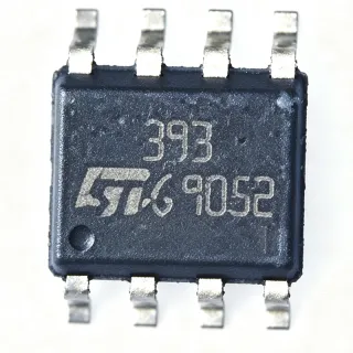
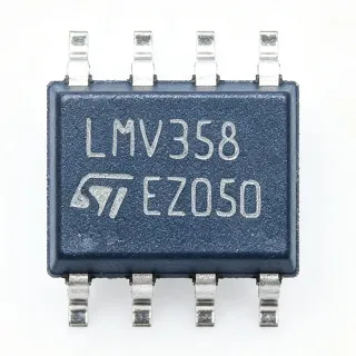
| Package | 14-pin DIP, 14-pin SOIC |
| Mounting Type | Through Hole, Surface Mount |
| RoHS Status | Compliant |
L9955 Pin Configuration
| Pin 1 | 1OUT — Output of amplifier 1 |
| Pin 2 | 1IN- — Inverting input of amplifier 1 |
| Pin 3 | 1IN+ — Non-inverting input of amplifier 1 |
| Pin 4 | VCC — Positive power supply |
| Pin 5 | 2IN+ — Non-inverting input of amplifier 2 |
| Pin 6 | 2IN- — Inverting input of amplifier 2 |
| Pin 7 | 2OUT — Output of amplifier 2 |
| Pin 8 | 3OUT — Output of amplifier 3 |
| Pin 9 | 3IN- — Inverting input of amplifier 3 |
| Pin 10 | 3IN+ — Non-inverting input of amplifier 3 |
| Pin 11 | GND — Ground (negative supply) |
| Pin 12 | 4IN+ — Non-inverting input of amplifier 4 |
| Pin 13 | 4IN- — Inverting input of amplifier 4 |
| Pin 14 | 4OUT — Output of amplifier 4 |
Typical Applications
L9955 is suitable for 6 applications: Battery-Powered Instruments, Sensor Signal Conditioning, Active Filters, Portable Medical Devices, Industrial Process Control, Automotive Electronics.
Battery-Powered Instruments
The L9955's low quiescent current of 0.4 mA per amplifier extends battery life in portable devices. In a typical battery monitoring circuit, the op-amp amplifies the voltage drop across a sense resistor, with the wide supply range accommodating 3V to 30V batteries. The rail-to-rail output allows direct connection to an ADC, and the low input bias current minimizes loading on high-impedance sensors. Compared to standard op-amps, the L9955 reduces power consumption by up to 40%, making it ideal for handheld multimeters and data loggers.
Recommended
Sensor Signal Conditioning
The L9955 is well-suited for conditioning signals from temperature, pressure, and strain sensors. Its low input offset voltage (2 mV) and low bias current (50 nA) ensure accurate amplification of small sensor outputs. In a bridge amplifier configuration, the L9955 provides the necessary gain and common-mode rejection. The wide supply range allows operation from unregulated supplies, and the output can drive the input of a microcontroller's ADC directly. For a thermocouple interface, the L9955 can amplify the microvolt-level signal to a usable range, with the low power consumption making it suitable for field transmitters.
Recommended
Active Filters
The L9955's 1 MHz unity-gain bandwidth and 0.5 V/µs slew rate make it suitable for active filters up to 100 kHz. In a second-order low-pass filter, the L9955 provides the necessary gain and phase response. The low quiescent current is advantageous in multi-stage filters where several op-amps are used. The wide supply range allows the filter to operate from a single 5V supply, and the rail-to-rail output maximizes the signal swing. For audio applications, the L9955 can implement tone control circuits with minimal distortion.
Recommended
Portable Medical Devices
In portable medical devices like glucose meters and pulse oximeters, the L9955 provides low-power signal conditioning. Its low quiescent current is critical for battery operation, and the wide supply range accommodates various battery chemistries. The low input offset voltage ensures accurate measurement of small biological signals. In a pulse oximeter, the L9955 amplifies the photodiode signal, and the rail-to-rail output allows direct interface with an ADC. The industrial temperature range ensures reliable operation in clinical environments.
Recommended
Industrial Process Control
The L9955 is used in industrial process control for signal conditioning and loop control. Its wide supply range (up to 30V) allows direct operation from 24V industrial supplies. The low offset voltage and bias current ensure accurate measurement of process variables like pressure and flow. In a 4-20 mA current loop transmitter, the L9955 can amplify the sensor signal and drive the loop. The industrial temperature range (-40°C to +85°C) makes it suitable for harsh environments. The low power consumption reduces heat dissipation in control cabinets.
Recommended
Automotive Electronics
In automotive applications, the L9955 can be used for sensor conditioning and control. Its wide supply range (up to 30V) handles automotive battery voltage variations, and the industrial temperature range covers under-hood environments. The low quiescent current is beneficial for always-on circuits like battery monitoring. In a tire pressure monitoring system, the L9955 amplifies the pressure sensor signal, and the rail-to-rail output interfaces with the MCU's ADC. For automotive-grade requirements, consider the LM2902, which is AEC-Q100 qualified.
Recommended
Recommended Products Summary
Engineering reference data for L9955 — comparison, design guidance, and compliance information.
Selection Guide
Comparison with Alternatives
| Parameter | This Product | LM324N | LM2902N | TLV2374IN | MC3403N |
|---|---|---|---|---|---|
| Package | 14-pin DIP, 14-pin SOIC | 14-pin DIP | 14-pin DIP | 14-pin DIP | 14-pin DIP |
| Brand | National Semiconductor | Texas Instruments | Texas Instruments | Texas Instruments | onsemi |
| Number of Channels | 4 | 4 | 4 | 4 | 4 |
| Supply Voltage Range (Single) | 3V to 30V | 3V to 32V | 3V to 26V | 2.7V to 16V | 3V to 36V |
| Quiescent Current per Amplifier | 0.4 mA | 0.7 mA | 0.7 mA | 0.55 mA | 0.5 mA |
| Unity-Gain Bandwidth | 1 MHz | 1.2 MHz | 1.2 MHz | 2.2 MHz | 1 MHz |
| Slew Rate | 0.5 V/µs | 0.5 V/µs | 0.5 V/µs | 2.4 V/µs | 0.6 V/µs |
| Input Offset Voltage | 2 mV | 2 mV | 2 mV | 2 mV | 2 mV |
Key Differentiators
- Lower quiescent current than LM324 (vs LM324N)
- Wider supply range than TLV2374 (vs TLV2374IN)
- Industrial temperature range (vs MC3403N)
Design Notes
For optimal performance, decouple the VCC pin with a 0.1 µF ceramic capacitor placed as close to the pin as possible. Additionally, a 10 µF electrolytic capacitor on the supply line can help filter low-frequency noise. The L9955's low quiescent current makes it suitable for battery-powered designs, but ensure the supply voltage does not exceed the absolute maximum rating of 32V.
For the SOIC package, use a ground plane to reduce noise and improve thermal performance. Keep the input traces short and shielded to minimize pickup. For the DIP package, a socket is recommended for prototyping. Ensure the PCB layout provides adequate spacing between high-impedance inputs and noisy digital traces.
Avoid driving loads below 2 kΩ directly, as this can cause excessive output current and distortion. For capacitive loads above 100 pF, add a series resistor (e.g., 50-100 Ω) to maintain stability. Also, ensure the input common-mode voltage stays within the specified range (0V to VCC - 1.5V) to avoid output phase reversal.
Compliance Information
RoHS compliant per National Semiconductor datasheet. Not AEC-Q100 qualified; use LM2902 for automotive.