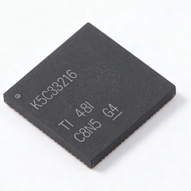
LMK5C33216RGCR - Ultra-Low Jitter Clock Synchronizer | TI
MPN: LMK5C33216RGCR ✓ Active| Qty | Unit Price | Extended |
|---|---|---|
| 1 | $52.07 | $52.07 |
| 10 | $48.5 | $485.00 |
| 100 | $42 | $4,200.00 |
| 500 | $38 | $19,000.00 |
| 1,000 | $35 | $35,000.00 |
LMK5C33216RGCR Overview
A clock synchronizer is a specialized timing IC that generates and aligns multiple clock signals to a reference, often cleaning jitter from noisy sources. In the hierarchy of timing components, a clock synchronizer sits above a simple PLL or clock generator, providing advanced features like hitless switching, holdover, and digital loop filtering. The LMK5C33216 is part of TI's LMK5C family, which targets 5G base stations, small cells, and other high-speed networking equipment where precise timing is critical for JESD204B data converters.
Key features include three DPLLs with programmable loop bandwidth from 0.01 Hz to 4 kHz, eliminating the need for external loop filters. The BAW APLL delivers exceptional jitter performance of 40 fs RMS, while the device also offers -116 dBc/Hz phase noise at 100 Hz offset. It supports JESD204B interface for direct connection to high-speed ADCs and DACs, and includes advanced reference clock selection with hitless switching to maintain synchronization during reference failures.
The LMK5C33216 integrates a flexible clock output architecture with multiple dividers and delays, allowing generation of various frequencies from a single reference. Its digital PLL architecture provides precise frequency synthesis and alignment, while the analog PLLs ensure low-noise output. The device is programmable via SPI or I2C, enabling dynamic reconfiguration in the field.
Typical applications include 5G NR base stations, remote radio heads, small cells, and test and measurement equipment. The device is also suitable for optical transport networks and data center switches requiring high-frequency, low-jitter clocks. Its wide output frequency range and low jitter make it ideal for JESD204B converter clocking.
When designing with the LMK5C33216, ensure proper power supply decoupling with low-ESR capacitors close to the VQFN pins. The exposed thermal pad must be soldered to a ground plane for adequate heat dissipation. Use the device's internal loop filters to simplify design, but verify loop bandwidth settings for your specific jitter transfer requirements.
Drop-in alternatives for LMK5C33216RGCR — same package, pin-to-pin compatible. Different-package parts requiring PCB rework are excluded.
Variants in this series
Same-series models that are drop-in compatible with LMK5C33216RGCR (same form factor and footprint) — differing in Interface, Package.
Quick Comparison Tool — Select alternative parts for side-by-side comparison:
LMK5C33216RGCT
📋 Reference alternative (not in catalog)
LMK5C33216RGC
📋 Reference alternative (not in catalog)
LMK5C33216RGCRQ1
📋 Reference alternative (not in catalog)
AD9528BCPZ
📋 Reference alternative (not in catalog)
LMK04828BISQ/NOPB
📋 Reference alternative (not in catalog)
LMK5C33216RGCR Specifications
| Output Frequency Range | 200 MHz, 1 GHz, 3 GHz |
| Number of DPLLs | 3 |
| Number of APLLs | 3 (paired with DPLLs) |
| BAW APLL Jitter | 40 fs RMS at 491.52 MHz |
| DPLL Loop Bandwidth | 0.01 Hz to 4 kHz |
| Phase Noise | -116 dBc/Hz at 100 Hz offset |
| Supply Voltage | 3.3 V |
| Package | VQFN (RGC) 64-pin |
| Operating Temperature Range | -40°C to +85°C |
| Interface | SPI or I2C |
| JESD204B Support | Yes |
| Hitless Switching | Yes |
| Reference Clock Selection | Advanced with hitless switching |
| External Loop Filters | Not required |
| RoHS Status | Compliant |
LMK5C33216RGCR Pin Configuration
| Pin 1 | VDD — Power supply (3.3V) |
| Pin 2 | GND — Ground |
| Pin 3 | CLKIN0 — Reference clock input 0 |
| Pin 4 | CLKIN1 — Reference clock input 1 |
| Pin 5 | CLKIN2 — Reference clock input 2 |
| Pin 6 | SDA — I2C data line |
| Pin 7 | SCL — I2C clock line |
| Pin 8 | SPI_CS — SPI chip select |
| Pin 9 | SPI_CLK — SPI clock |
| Pin 10 | SPI_DIN — SPI data input |
| Pin 11 | SPI_DOUT — SPI data output |
| Pin 12 | OUT0 — Clock output 0 |
| Pin 13 | OUT1 — Clock output 1 |
| Pin 14 | OUT2 — Clock output 2 |
| Pin 15 | OUT3 — Clock output 3 |
| Pin 16 | OUT4 — Clock output 4 |
| Pin 17 | OUT5 — Clock output 5 |
| Pin 18 | OUT6 — Clock output 6 |
| Pin 19 | OUT7 — Clock output 7 |
| Pin 20 | OUT8 — Clock output 8 |
| Pin 21 | OUT9 — Clock output 9 |
| Pin 22 | OUT10 — Clock output 10 |
| Pin 23 | OUT11 — Clock output 11 |
| Pin 24 | OUT12 — Clock output 12 |
| Pin 25 | OUT13 — Clock output 13 |
| Pin 26 | OUT14 — Clock output 14 |
| Pin 27 | OUT15 — Clock output 15 |
| Pin 28 | VDD — Power supply (3.3V) |
| Pin 29 | GND — Ground |
| Pin 30 | VDD — Power supply (3.3V) |
| Pin 31 | GND — Ground |
| Pin 32 | VDD — Power supply (3.3V) |
| Pin 33 | GND — Ground |
| Pin 34 | VDD — Power supply (3.3V) |
| Pin 35 | GND — Ground |
| Pin 36 | VDD — Power supply (3.3V) |
| Pin 37 | GND — Ground |
| Pin 38 | VDD — Power supply (3.3V) |
| Pin 39 | GND — Ground |
| Pin 40 | VDD — Power supply (3.3V) |
| Pin 41 | GND — Ground |
| Pin 42 | VDD — Power supply (3.3V) |
| Pin 43 | GND — Ground |
| Pin 44 | VDD — Power supply (3.3V) |
| Pin 45 | GND — Ground |
| Pin 46 | VDD — Power supply (3.3V) |
| Pin 47 | GND — Ground |
| Pin 48 | VDD — Power supply (3.3V) |
| Pin 49 | GND — Ground |
| Pin 50 | VDD — Power supply (3.3V) |
| Pin 51 | GND — Ground |
| Pin 52 | VDD — Power supply (3.3V) |
| Pin 53 | GND — Ground |
| Pin 54 | VDD — Power supply (3.3V) |
| Pin 55 | GND — Ground |
| Pin 56 | VDD — Power supply (3.3V) |
| Pin 57 | GND — Ground |
| Pin 58 | VDD — Power supply (3.3V) |
| Pin 59 | GND — Ground |
| Pin 60 | VDD — Power supply (3.3V) |
| Pin 61 | GND — Ground |
| Pin 62 | VDD — Power supply (3.3V) |
| Pin 63 | GND — Ground |
| Pin 64 | VDD — Power supply (3.3V) |
Typical Applications
LMK5C33216RGCR is suitable for 6 applications: 5G Base Station Clocking, JESD204B Converter Clocking, Small Cell Backhaul, Optical Transport Networks, Test and Measurement Equipment, Data Center Switches.
5G Base Station Clocking
The LMK5C33216RGCR provides ultra-low jitter clocks for 5G base station transceivers. Its 40 fs RMS jitter and JESD204B support ensure precise synchronization of high-speed ADCs and DACs, improving signal quality and reducing bit errors. The device's three DPLLs allow independent clock domains for different radio paths, while hitless switching maintains timing during reference failures.
Recommended
JESD204B Converter Clocking
The LMK5C33216RGCR is ideal for clocking JESD204B data converters in wireless and wireline systems. Its low jitter (40 fs RMS) and support for multiple output frequencies (up to 3 GHz) ensure reliable data conversion. The device's integrated DPLLs provide flexible frequency synthesis, while the JESD204B interface simplifies connection to converters, reducing design complexity.
Recommended
Small Cell Backhaul
In small cell backhaul, the LMK5C33216RGCR provides precise timing for Ethernet and wireless links. Its ultra-low jitter and hitless switching ensure seamless synchronization, critical for maintaining quality of service. The device's compact VQFN package and integrated loop filters reduce board space, making it suitable for space-constrained small cell designs.
Recommended
Optical Transport Networks
The LMK5C33216RGCR is used in optical transport networks to generate low-jitter clocks for high-speed optical modules. Its 40 fs RMS jitter and support for frequencies up to 3 GHz meet the stringent requirements of 100G/400G optical links. The device's three DPLLs enable independent clocking for different channels, while its low phase noise improves signal integrity.
Recommended
Test and Measurement Equipment
The LMK5C33216RGCR provides precise, low-jitter clocks for test and measurement instruments such as oscilloscopes and signal generators. Its programmable DPLLs allow fine-tuning of output frequencies, while its low phase noise ensures accurate measurements. The device's SPI/I2C interface enables easy configuration in automated test systems.
Recommended
Data Center Switches
In data center switches, the LMK5C33216RGCR generates low-jitter clocks for high-speed SerDes and network processors. Its ultra-low jitter (40 fs RMS) and support for multiple output frequencies ensure reliable data transmission at 100G/400G rates. The device's hitless switching maintains synchronization during reference changes, critical for network uptime.
Recommended
Recommended Products Summary
Engineering reference data for LMK5C33216RGCR — comparison, design guidance, and compliance information.
Selection Guide
Comparison with Alternatives
| Parameter | This Product | LMK5C33216RGCT | LMK5C33216RGC | LMK5C33216RGCRQ1 | AD9528BCPZ | LMK04828BISQ/NOPB |
|---|---|---|---|---|---|---|
| Package | VQFN (RGC) 64-pin | VQFN (RGC) 64-pin | VQFN (RGC) 64-pin | VQFN (RGC) 64-pin | LFCSP-48 | WQFN-64 |
| Brand | Texas Instruments | Texas Instruments | Texas Instruments | Texas Instruments | Analog Devices | Texas Instruments |
| Output Frequency Range | 200 MHz, 1 GHz, 3 GHz | 200 MHz, 1 GHz, 3 GHz | 200 MHz, 1 GHz, 3 GHz | 200 MHz, 1 GHz, 3 GHz | 1 GHz | 3.1 GHz |
| Jitter (RMS) | 40 fs at 491.52 MHz | 40 fs at 491.52 MHz | 40 fs at 491.52 MHz | 40 fs at 491.52 MHz | 100 fs | 111 fs |
| Number of DPLLs | 3 | 3 | 3 | 3 | 2 | 2 |
| JESD204B Support | Yes | Yes | Yes | Yes | Yes | Yes |
| Supply Voltage | 3.3V | 3.3V | 3.3V | 3.3V | 3.3V | 3.3V |
| Operating Temperature Range | -40°C to +85°C | -40°C to +85°C | -40°C to +85°C | -40°C to +105°C | -40°C to +85°C | -40°C to +85°C |
Key Differentiators
- Ultra-low jitter of 40 fs RMS (vs AD9528BCPZ)
- Three DPLLs with programmable loop bandwidth (vs LMK04828BISQ/NOPB)
- Integrated BAW APLL (vs AD9528BCPZ)
Design Notes
The LMK5C33216RGCR requires a clean 3.3V supply. Use low-ESR ceramic capacitors (e.g., 0.1uF and 10uF) placed close to each VDD pin to minimize power supply noise. A ferrite bead in series with the supply can further isolate high-frequency noise from the clock outputs.
The exposed thermal pad on the VQFN package must be soldered to a ground plane for proper heat dissipation. Use multiple vias under the pad to connect to inner ground layers. Ensure the ground plane is continuous and has low impedance to avoid ground bounce.
Route clock output traces with controlled impedance (e.g., 50 ohms) and keep them as short as possible to minimize reflections and crosstalk. Avoid routing clock traces near noisy digital signals. Use ground vias around clock traces to provide shielding.
Compliance Information
RoHS compliant per TI product page. Not AEC-Q100 qualified; automotive variant LMK5C33216RGCRQ1 is available.







