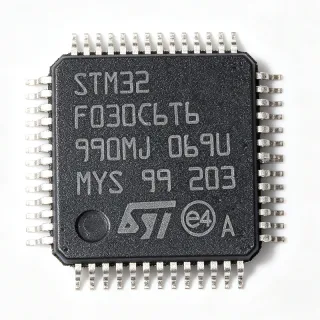
MC9S08DZ32ACLF - 32KB Flash 8-bit CAN MCU, 40MHz LQFP-48 | NXP
MPN: MC9S08DZ32ACLF ✗ End of Life| Qty | Unit Price | Extended |
|---|---|---|
| 1 | $5.92 | $5.92 |
| 10 | $5.45 | $54.50 |
| 100 | $4.78 | $478.00 |
| 500 | $4.21 | $2,105.00 |
| 1,000 | $3.74 | $3,740.00 |
MC9S08DZ32ACLF Overview
An 8-bit microcontroller (MCU) is a single-chip computer that integrates a CPU, RAM, program memory (Flash), and peripheral interfaces (timers, ADC, communication ports) into one device. Within the broader hierarchy, the MC9S08DZ32ACLF belongs to the HCS08 sub-family of the S08 8-bit line, which itself falls under microcontrollers -> microprocessors and logic -> semiconductor ICs. The part is part of NXP's S08DZ series that combines CAN 2.0A/B, LIN, SCI, SPI and I2C peripherals with embedded Flash and EEPROM.
Key features include 32 KB of on-chip Flash program memory with in-application programming support, 2 KB of SRAM, on-chip EEPROM for data storage, a 24-channel 12-bit ADC with 2.5 µs conversion time, an analog comparator, and up to 32 interrupt sources. The integrated MSCAN (CAN 2.0 A/B) and LIN-master-capable SCI make it well suited for vehicle body and industrial sensor networks. Background debug mode (BGND) and on-chip emulation are available through the standard HCS08 debug interface.
Architecturally the part uses the enhanced HCS08 CPU core running at 40 MHz with a 20 MHz internal bus, retains the HC08 instruction set for code compatibility and adds the BGND instruction for debug. The integrated voltage regulator, low-power run/wait/stop modes, and a wide supply range (2.7 V to 5.5 V) support both 3.3 V and 5 V systems typical of automotive body controllers.
Typical applications include automotive body and chassis CAN/LIN nodes, industrial sensor and actuator modules, HVAC controllers, instrument cluster sub-modules, and general-purpose 8-bit embedded control with on-chip CAN. The combination of 32 KB Flash and 2 KB RAM is sufficient for typical CAN-stack plus application firmware.
When designing with the MC9S08DZ32ACLF, ensure that the IRQ, RESET and BKGD/MS pins are routed correctly for the chosen debug tool (P&E Multilink or equivalent). Decouple VDD/VSS pairs close to the package and follow NXP's reference layout for the 48-LQFP to avoid ESD and EMC issues on CAN bus pins.
This page synthesizes distributor pricing, drop-in alternatives and practical design notes not found in the manufacturer datasheet alone.
Drop-in alternatives for MC9S08DZ32ACLF — same package, pin-to-pin compatible. Different-package parts requiring PCB rework are excluded.
Variants in this series
Same-series models that are drop-in compatible with MC9S08DZ32ACLF (same form factor and footprint) — differing in Package, CAN, Core, Supply Voltage, RoHS Status.
Quick Comparison Tool — Select alternative parts for side-by-side comparison:
S9S08DZ32F2VLCR
✅ Drop-In ⚠️ Specs Unverified✓ In Stock
$4.2 / Unit
View Datasheet →S9S08DZ96F2VLF
✅ Drop-In ⚠️ Specs Unverified✓ In Stock
$6.55 / Unit
View Datasheet →S9S08DZ60F2MLHR
✅ Drop-In ⚠️ Specs Unverified✓ In Stock
$4.08 / Unit
View Datasheet →MC9S08DZ60ACLF
✅ Drop-In ⚠️ Specs Unverified✓ In Stock
$6.85 / Unit
View Datasheet →MC9S08DZ32AMLF
✅ Drop-In✓ In Stock
$2.75 / Unit
View Datasheet →MC9S08DZ32ACLF Maximum Ratings & Electrical Characteristics
| Core | HCS08 (S08) 8-bit CPU |
| Maximum CPU Frequency | 40 MHz (20 MHz bus) |
| Instruction Set | HC08 with BGND added |
| Program Memory (Flash) | 32 KB |
| RAM | 2 KB |
| Package | 48-pin LQFP (7x7 mm) |
| Supply Voltage | 2.7 V to 5.5 V (3.3 V / 5 V) |
| ADC | 24-channel, 12-bit, 2.5 us conversion |
| Analog Comparator | Yes (on-chip) |
| CAN | MSCAN (CAN 2.0 A/B) |
| SCI / LIN | SCI with LIN master support |
| SPI | Yes (on-chip) |
| I2C | Yes (on-chip) |
| Interrupt Sources | Up to 32 |
| Debug Interface | Background Debug Mode (BDM) / on-chip emulation |
| Operating Temperature | -40C to +85C (automotive grade available) |
| Mounting Type | Surface Mount |
MC9S08DZ32ACLF Pin Configuration
| Pin 1 | PTD6/TPM1CH2 — Port D I/O / TPM1 channel 2 |
| Pin 2 | PTD7/KBI3P7 — Port D I/O / keyboard interrupt |
| Pin 3 | VDD — Supply voltage (2.7 V to 5.5 V) |
| Pin 4 | VSS — Ground |
| Pin 5 | PTB0/ADP0 — Port B I/O / ADC channel 0 |
| Pin 6 | PTB1/ADP1 — Port B I/O / ADC channel 1 |
| Pin 7 | PTB2/ADP2 — Port B I/O / ADC channel 2 |
| Pin 8 | PTB3/ADP3 — Port B I/O / ADC channel 3 |
| Pin 9 | PTB4/ADP4 — Port B I/O / ADC channel 4 |
| Pin 10 | PTB5/ADP5 — Port B I/O / ADC channel 5 |
| Pin 11 | PTB6/ADP6 — Port B I/O / ADC channel 6 |
| Pin 12 | PTB7/ADP7 — Port B I/O / ADC channel 7 |
| Pin 13 | PTA0/ADP8 — Port A I/O / ADC channel 8 |
| Pin 14 | PTA1/ADP9 — Port A I/O / ADC channel 9 |
| Pin 15 | PTA2/ADP10 — Port A I/O / ADC channel 10 |
| Pin 16 | PTA3/ADP11 — Port A I/O / ADC channel 11 |
| Pin 17 | PTA4/ADP12 — Port A I/O / ADC channel 12 |
| Pin 18 | PTA5/ADP13 — Port A I/O / ADC channel 13 |
| Pin 19 | PTA6/ADP14 — Port A I/O / ADC channel 14 |
| Pin 20 | PTA7/ADP15 — Port A I/O / ADC channel 15 |
| Pin 21 | VDDA — Analog supply voltage |
| Pin 22 | VSSA — Analog ground |
| Pin 23 | PTC0/ADP16 — Port C I/O / ADC channel 16 |
| Pin 24 | PTC1/ADP17 — Port C I/O / ADC channel 17 |
| Pin 25 | PTC2/ADP18 — Port C I/O / ADC channel 18 |
| Pin 26 | PTC3/ADP19 — Port C I/O / ADC channel 19 |
| Pin 27 | PTC4/ADP20 — Port C I/O / ADC channel 20 |
| Pin 28 | PTC5/ADP21 — Port C I/O / ADC channel 21 |
| Pin 29 | PTC6/ADP22 — Port C I/O / ADC channel 22 |
| Pin 30 | PTC7/ADP23 — Port C I/O / ADC channel 23 |
| Pin 31 | PTE0/CANTx — Port E I/O / MSCAN transmit |
| Pin 32 | PTE1/CANRx — Port E I/O / MSCAN receive |
| Pin 33 | PTE2/SCETx — Port E I/O / SCI transmit (LIN) |
| Pin 34 | PTE3/SCERx — Port E I/O / SCI receive (LIN) |
| Pin 35 | PTE4/SPSCK — Port E I/O / SPI clock |
| Pin 36 | PTE5/MOSI — Port E I/O / SPI MOSI |
| Pin 37 | PTE6/MISO — Port E I/O / SPI MISO |
| Pin 38 | PTE7/SS — Port E I/O / SPI slave select |
| Pin 39 | PTF0/ACMPO — Port F I/O / analog comparator output |
| Pin 40 | PTF1/ACMPP — Port F I/O / analog comparator positive input |
| Pin 41 | PTF2/ACMPM — Port F I/O / analog comparator negative input |
| Pin 42 | PTF3 — Port F I/O |
| Pin 43 | PTF4 — Port F I/O |
| Pin 44 | PTF5 — Port F I/O |
| Pin 45 | PTF6 — Port F I/O |
| Pin 46 | PTF7 — Port F I/O |
| Pin 47 | BKGD/MS — Background Debug Mode / Mode Select |
| Pin 48 | RESET — Reset input (active low) |
Typical Applications
MC9S08DZ32ACLF is suitable for 6 applications: Automotive Body Control Modules (CAN/LIN), Industrial Sensor and Actuator Nodes, HVAC Control Modules, Instrument Cluster Sub-modules, Low-Cost CAN Node Replacement Boards, General 8-bit Embedded Control with CAN.
Automotive Body Control Modules (CAN/LIN)
The MC9S08DZ32ACLF is designed for in-vehicle CAN and LIN networks thanks to its on-chip MSCAN (CAN 2.0 A/B) controller and LIN-master capable SCI. With 32 KB Flash it accommodates a CANopen or CCP/UDS stack plus body-control firmware for lighting, door, seat and HVAC functions. The 48-LQFP footprint supports compact body and chassis ECUs where the part acts as a CAN/LIN node sitting on a 5 V or 3.3 V bus. Compared with discrete CAN transceivers plus external EEPROM, the integrated 12-bit ADC and on-chip EEPROM reduce BOM by several dollars per node.
Recommended
Industrial Sensor and Actuator Nodes
The MC9S08DZ32ACLF suits industrial sensor hubs and actuator drivers needing industrial CANopen or DeviceNet connectivity at a low BOM cost. The 24-channel 12-bit ADC with 2.5 µs conversion handles analog sensor inputs (temperature, pressure, position), while the SPI and I2C interfaces connect to digital front-ends and DACs. Running at 40 MHz with 2 KB RAM, the part is fast enough to manage a CANopen stack plus application timing. Its wide 2.7 V to 5.5 V supply lets the same MCU work on 24 V industrial rails when paired with a switching pre-regulator.
Recommended
HVAC Control Modules
HVAC modules combine temperature sensing, fan/blower drive, and CAN communication with the vehicle body network. The MC9S08DZ32ACLF is a good fit because its 24-channel 12-bit ADC reads multiple thermistor inputs in parallel, its PWM/timer blocks drive TRIAC or FET-based fan drivers, and its MSCAN controller links to the body CAN bus. The 32 KB Flash is ample for PID blower control plus diagnostics; the on-chip EEPROM stores calibration data without external memory.
Recommended
Instrument Cluster Sub-modules
The MC9S08DZ32ACLF is used as a sub-MCU inside instrument clusters to drive stepper-motor gauge indicators and read cluster sensors via CAN. The HCS08 core and 20 MHz bus handle display multiplexing, while the SPI interface connects to LED drivers and the MSCAN controller talks to the body ECU. With on-chip EEPROM, gauge calibration data and DTCs can be kept locally without external NVM, simplifying PCB layout. Compared with full-cluster processors, the S08DZ family offers the right balance of CAN, EEPROM and ADC at minimal cost.
Recommended
Low-Cost CAN Node Replacement Boards
Field retrofits and aftermarket accessories often need a small, low-cost CAN controller with enough Flash for a slim command set. The MC9S08DZ32ACLF fits this use because the 32 KB Flash can hold a minimal UDS/CCP stack plus the application firmware, and the 48-LQFP can be placed on a small PCB alongside a TJA1042 CAN transceiver. The on-chip EEPROM stores node ID and configuration without an external NVM part.
Recommended
General 8-bit Embedded Control with CAN
Beyond automotive, the MC9S08DZ32ACLF is also a general 8-bit MCU for any application needing CAN plus modest processing - e.g., elevator controllers, building automation nodes, agricultural equipment and small motor controls. The combination of 40 MHz CPU, 32 KB Flash, 2 KB RAM and on-chip EEPROM gives designers enough headroom for a CANopen or DeviceNet stack while keeping the bill of materials low. The HCS08 core's HC08-compatible instruction set eases porting from older Freescale designs.
Recommended
Recommended Products Summary
Engineering reference data for MC9S08DZ32ACLF — comparison, design guidance, and compliance information.
Selection Guide
Comparison with Alternatives
| Parameter | This Product | S9S08DZ32F2VLCR | S9S08DZ96F2VLF | S9S08DZ60F2MLHR | MC9S08DZ60ACLF | MC9S08DZ32AMLF |
|---|---|---|---|---|---|---|
| Brand | NXP Semiconductors | NXP Semiconductors | NXP Semiconductors | NXP Semiconductors | NXP Semiconductors | NXP Semiconductors |
| Package | LQFP-48 (7x7 mm) | LQFP-48 - same | LQFP-48 - same | LQFP-48 - same | LQFP-48 - same | LQFP-48 - same |
| Flash | 32 KB | 32 KB | 96 KB | 60 KB | 60 KB | 32 KB |
| RAM | 2 KB | 2 KB | 4 KB | 3 KB | 3 KB | 2 KB |
| CPU Frequency | 40 MHz | 40 MHz | 40 MHz | 40 MHz | 40 MHz | 40 MHz |
| CAN (MSCAN) | Yes | Yes | Yes | Yes | Yes | Yes |
| LIN (SCI) | Yes | Yes | Yes | Yes | Yes | Yes |
| ADC Channels / Resolution | 24 ch / 12-bit | 24 ch / 12-bit | 24 ch / 12-bit | 24 ch / 12-bit | 24 ch / 12-bit | 24 ch / 12-bit |
| Lifecycle Status | NRND | Active | Active | Active | NRND | NRND |
Key Differentiators
- Integrated MSCAN + LIN in a single 8-bit MCU (vs MC9S08AC32CFGE)
- Same-family 32 KB Flash successor in active production (vs S9S08DZ32F2VLCR)
- Triple Flash headroom option in the same footprint (vs S9S08DZ96F2VLF)
- 24-channel 12-bit ADC for sensor-rich designs (vs MC9S08AW60CFGE)
Design Notes
Decouple every VDD/VSS pair close to the LQFP-48 leads with a 100 nF plus 10 nF ceramic capacitor pair, and place a single 10 µF bulk capacitor near the package. The on-chip voltage regulator requires VDD within 2.7 V to 5.5 V; out-of-spec supply causes Flash corruption and unrecoverable resets. Tie unused VDD pins together and to a single supply rail.
Route the BKGD/MS pin to a dedicated debug header that is short and isolated from switching traces. Long BKGD traces pick up noise and fail to enter Background Debug Mode reliably. Do not pull BKGD high with a strong pull-up; a 10 kΩ pull-up to VDD is sufficient and the debug tool will drive it as required.
Route CANH/CANL traces on the MCU side as a 2-wire differential pair with ~50 Ω impedance, and place the external CAN transceiver (e.g. TJA1042) within 50 mm of the PTE0/PTE1 pins. Keep both lines away from switching converters and clock traces to maintain CAN EMC margins. Add a 4.7 nF split-termination capacitor at the bus end for ISO 11898 compliance.
Estimated: at 40 MHz CPU and 5 V VDD with all peripherals active, the die dissipates roughly 40 mW to 60 mW. The 48-LQFP has θJA ≈ 70 °C/W on a JEDEC 4-layer test board, so a 60 mW dissipation only raises junction temperature ~4 °C above ambient. No heatsink is required; an uninterrupted copper ground pour under the exposed pad is recommended for production.
Compliance Information
RoHS, REACH, AEC-Q100 and lead-free compliance per NXP product page (https://www.nxp.com/part/MC9S08DZ32ACLF). Automotive-grade AEC-Q100 qualification noted as 'automotive' in the NXP datasheet family overview.