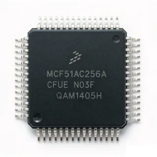
MCF51JM64VQH - ColdFire V1 32-bit MCU, 64KB Flash, 50MHz | NXP
MPN: MCF51JM64VQH ✓ Active| Qty | Unit Price | Extended |
|---|---|---|
| 1 | $8.21 | $8.21 |
| 10 | $7.39 | $73.90 |
| 100 | $6.57 | $657.00 |
| 500 | $5.91 | $2,955.00 |
| 1,000 | $5.25 | $5,250.00 |
MCF51JM64VQH Overview
A microcontroller (MCU) is a single-chip computer integrating a CPU core, program and data memory, peripherals, and I/O. ColdFire V1 is a 32-bit reduced instruction set computing (RISC) architecture derived from the original ColdFire family, optimized for embedded deterministic control with small code size and low power. Within the broader semiconductor taxonomy, the MCF51JM64 belongs to the microcontrollers hierarchy (microcontroller -> 32-bit MCU -> embedded processor -> semiconductor IC). The Flexis positioning is significant: a designer can prototype on a JM device and migrate to an S08 pin-compatible MCU without a full PCB redesign.
Key specifications include a 32-bit ColdFire V1 core at 50 MHz, 64 KB flash program memory, 8 KB SRAM, an 8-channel 12-bit ADC, timers (including PWM channels), SPI, I²C, and UART communication peripherals, plus a USB 2.0 Full-Speed (12 Mbps) device/host/on-the-go controller. The 64-pin LQFP package supports industrial-grade -40°C to +105°C operation. The integrated USB controller with on-chip transceiver eliminates external PHY requirements for many USB device applications.
Architecturally, the MCF51JM64 uses a Harvard-oriented ColdFire V1 core with a single-cycle 32-bit ALU, hardware multiply/accumulate, and a tightly-coupled peripheral bus. The Flexis shared-peripheral philosophy with the S08 family means the same peripheral IP blocks (ADC, timers, communications modules) appear on both families, allowing identical firmware drivers across 8-bit and 32-bit performance tiers.
Typical applications include industrial control and sensor conditioning, building automation and HVAC controllers, USB peripherals such as HID-class human-interface devices, low-end medical instruments, consumer electronics requiring a USB device interface, and small-form-factor embedded control boards. The integrated USB 2.0 FS OTG controller also makes the part suitable for point-of-sale terminals and cable replacement use cases.
Designers should note that the MCF51JM family is being maintained primarily for legacy and industrial embedded designs, and lifecycle support should be confirmed against the latest NXP product change notifications. When planning new designs, evaluate the MCF51JM128 (128 KB flash) or Kinetis E series as longer-term alternatives while keeping the JM family in scope for proven, qualified, and stable code reuse.
This page synthesizes distributor pricing, parametric comparison, and Flexis migration notes not found in the manufacturer datasheet alone.
Drop-in alternatives for MCF51JM64VQH — same package, pin-to-pin compatible. Different-package parts requiring PCB rework are excluded.
Variants in this series
Same-series models that are drop-in compatible with MCF51JM64VQH (same form factor and footprint) — differing in Package, Program Memory Size, Architecture, Connectivity, Series.
Quick Comparison Tool — Select alternative parts for side-by-side comparison:
MCF51JM128VQH
✅ Drop-In📋 Reference alternative (not in catalog)
MKE02Z64VQH4
✅ Drop-In📋 Reference alternative (not in catalog)
MKE02Z64VLD2
✅ Drop-In ⚠️ Specs Unverified✓ In Stock
$3.62 / Unit
View Datasheet →MKE04Z64VLK4R
✅ Drop-In✓ In Stock
$2.24 / Unit
View Datasheet →MKL26Z32VLH4
✅ Drop-In ⚠️ Specs Unverified✓ In Stock
$2.98 / Unit
View Datasheet →MCF51JM64VQH Maximum Ratings & Electrical Characteristics
| Manufacturer | NXP Semiconductors |
| Core | ColdFire V1 (32-bit RISC) |
| Processor Series | MCF51JM (Flexis) |
| Maximum CPU Frequency | 50 MHz |
| Program Memory Size | 64 KB (64K x 8) FLASH |
| RAM Size | 8 KB |
| Data Bus Width | 32 bit |
| Package | 64-LQFP (14x14 mm) |
| Pin Count | 64 |
| Mounting Type | Surface Mount |
| USB Controller | USB 2.0 Full-Speed Device/Host/OTG with on-chip transceiver |
| ADC | 8-channel, 12-bit SAR |
| Communication Peripherals | SPI, I2C, USB FS OTG |
| Family | Flexis (pin-compatible with S08 family) |
MCF51JM64VQH Pin Configuration
| Pin 1 | PTE0/TxD1 — Port E bit 0 / UART1 transmit |
| Pin 2 | PTE1/RxD1 — Port E bit 1 / UART1 receive |
| Pin 3 | PTE2 — Port E bit 2 |
| Pin 4 | PTE3 — Port E bit 3 |
| Pin 5 | PTE4 — Port E bit 4 |
| Pin 6 | PTE5 — Port E bit 5 |
| Pin 7 | PTE6 — Port E bit 6 |
| Pin 8 | PTE7 — Port E bit 7 |
| Pin 9 | VSS — Ground |
| Pin 10 | PTF0 — Port F bit 0 |
| Pin 11 | PTF1 — Port F bit 1 |
| Pin 12 | PTF2 — Port F bit 2 |
| Pin 13 | PTF3 — Port F bit 3 |
| Pin 14 | PTF4 — Port F bit 4 |
| Pin 15 | PTF5 — Port F bit 5 |
| Pin 16 | PTF6 — Port F bit 6 |
| Pin 17 | PTF7 — Port F bit 7 |
| Pin 18 | VDD — Digital supply voltage |
| Pin 19 | USB_DP — USB D+ data line |
| Pin 20 | USB_DM — USB D- data line |
| Pin 21 | VREGIN — USB regulator input |
| Pin 22 | VOUT33 — USB 3.3V regulator output |
| Pin 23 | PTG0 — Port G bit 0 |
| Pin 24 | PTG1 — Port G bit 1 |
| Pin 25 | PTG2 — Port G bit 2 |
| Pin 26 | PTG3 — Port G bit 3 |
| Pin 27 | PTA0 — Port A bit 0 |
| Pin 28 | PTA1 — Port A bit 1 |
| Pin 29 | PTA2 — Port A bit 2 |
| Pin 30 | PTA3 — Port A bit 3 |
| Pin 31 | PTA4 — Port A bit 4 |
| Pin 32 | PTA5 — Port A bit 5 |
| Pin 33 | PTA6 — Port A bit 6 |
| Pin 34 | PTA7 — Port A bit 7 |
| Pin 35 | PTB0 — Port B bit 0 |
| Pin 36 | PTB1 — Port B bit 1 |
| Pin 37 | PTB2 — Port B bit 2 |
| Pin 38 | PTB3 — Port B bit 3 |
| Pin 39 | PTB4 — Port B bit 4 |
| Pin 40 | PTB5 — Port B bit 5 |
| Pin 41 | PTB6 — Port B bit 6 |
| Pin 42 | PTB7 — Port B bit 7 |
| Pin 43 | PTC0 — Port C bit 0 |
| Pin 44 | PTC1 — Port C bit 1 |
| Pin 45 | PTC2 — Port C bit 2 |
| Pin 46 | PTC3 — Port C bit 3 |
| Pin 47 | PTC4 — Port C bit 4 |
| Pin 48 | PTC5 — Port C bit 5 |
| Pin 49 | PTC6 — Port C bit 6 |
| Pin 50 | PTC7 — Port C bit 7 |
| Pin 51 | PTD0 — Port D bit 0 |
| Pin 52 | PTD1 — Port D bit 1 |
| Pin 53 | PTD2 — Port D bit 2 |
| Pin 54 | PTD3 — Port D bit 3 |
| Pin 55 | PTD4 — Port D bit 4 |
| Pin 56 | PTD5 — Port D bit 5 |
| Pin 57 | PTD6 — Port D bit 6 |
| Pin 58 | PTD7 — Port D bit 7 |
| Pin 59 | RESET — Active-low reset input |
| Pin 60 | EXTAL — External crystal/oscillator input |
| Pin 61 | XTAL — External crystal output |
| Pin 62 | TEST — Test mode (tie to ground in normal use) |
| Pin 63 | BKGD — Background debug mode |
| Pin 64 | VDDA/VREFH — Analog supply / ADC reference high |
Typical Applications
MCF51JM64VQH is suitable for 6 applications: USB HID / Human-Interface Device, Industrial Sensor Conditioning, Building Automation / HVAC, USB-to-Serial Bridge / Point-of-Sale Terminal, Low-End Medical Instruments, Consumer USB Device / Embedded Control.
USB HID / Human-Interface Device
The MCF51JM64VQH's integrated USB 2.0 Full-Speed Device/Host/OTG controller with on-chip transceiver suits HID and CDC-class peripherals where BOM minimalism is critical. The 50 MHz ColdFire V1 core runs typical 8-16 KB USB HID/CDC stacks with 32-48 KB headroom for application logic in 64 KB flash. Unlike external-USB USB MCU solutions, the JM64 eliminates external PHY parts. Pin-compatible migration to the Kinetis E family (MKE02Z64VQH4) lets designers swap cores while reusing PCBs and drivers.
Recommended
Industrial Sensor Conditioning
The 8-channel 12-bit SAR ADC and 50 MHz ColdFire V1 core make the MCF51JM64VQH suitable for multi-channel sensor-conditioning applications such as process transmitters, multi-zone HVAC controllers, and factory-floor analog front-end nodes. With 50 MHz performance, the JM64 can sample 8 channels at 10 kHz with on-chip averaging and still meet deterministic control loops. The 64-LQFP industrial package supports harsh-environment deployment with proper PCB layout. Flexis compatibility lets engineers migrate to the S08 family for lower-cost pin-compatible daughterboards.
Recommended
Building Automation / HVAC
The MCF51JM64VQH fits building-automation gateways and HVAC zone controllers where 8 KB SRAM holds modest control tables and the ColdFire V1 core executes 50 MHz control loops. The integrated USB 2.0 FS controller supports commissioning ports, and the 12-bit ADC reads thermistor and 0-10 V sensor inputs. Unlike smaller 8-bit S08 alternatives, the JM64 gives 32-bit headroom for future firmware features while remaining pin-compatible. PCB layout benefits from industrial-grade 64-LQFP thermal handling.
Recommended
USB-to-Serial Bridge / Point-of-Sale Terminal
The MCF51JM64VQH's USB 2.0 FS OTG controller with on-chip transceiver enables cable-replacement and POS terminal applications without external PHY. The 50 MHz ColdFire V1 core runs USB CDC stacks plus protocol translation, and the 64 KB flash holds descriptors and application code. Unlike USB-capable 8-bit MCUs, the JM64's 32-bit ALU accelerates descriptor parsing and bulk-packet reformatting. Designers benefit from a single-chip USB bridge solution.
Recommended
Low-End Medical Instruments
The MCF51JM64VQH suits low-end patient-monitoring peripherals, electronic stethoscopes, and USB-connected diagnostic accessories where 64 KB flash and 50 MHz ColdFire V1 performance are sufficient. The 12-bit ADC reads analog sensor channels at medical-grade resolution, and the 64-LQFP industrial package supports medical-device PCB layouts. Flexis shared-peripheral compatibility lets designers move to S08 family pin-compatible daughterboards for cost-sensitive variants.
Recommended
Consumer USB Device / Embedded Control
The MCF51JM64VQH targets compact consumer USB devices and small embedded control boards where a single-chip MCU with integrated USB simplifies BOM. The 50 MHz ColdFire V1 core plus 8 KB SRAM executes typical consumer device firmware, and the 12-bit ADC adds analog monitoring. Unlike external-USB consumer MCU solutions, the JM64 integrates PHY. NXP's Flexis compatibility ensures proven firmware portability to S08 family pin-compatible variants for cost reduction.
Recommended
Recommended Products Summary
Engineering reference data for MCF51JM64VQH — comparison, design guidance, and compliance information.
Selection Guide
Comparison with Alternatives
| Parameter | This Product | MCF51JM128VQH | MKE02Z64VQH4 | MKE02Z64VLD2 | MKE04Z64VLK4R | MKL26Z32VLH4 |
|---|---|---|---|---|---|---|
| Brand | NXP Semiconductors | NXP Semiconductors | NXP Semiconductors | NXP Semiconductors | NXP Semiconductors | NXP Semiconductors |
| Package | 64-LQFP (14x14 mm) | 64-LQFP (14x14 mm) - same | 64-LQFP - same | 64-LQFP - same | 64-LQFP - same | 64-LQFP - same |
| Core Architecture | ColdFire V1 (32-bit RISC) | ColdFire V1 (32-bit RISC) | ARM Cortex-M0+ (32-bit) | ARM Cortex-M0+ (32-bit) | ARM Cortex-M0+ (32-bit) | ARM Cortex-M0+ (32-bit) |
| Flash Memory | 64 KB | 128 KB | 64 KB | 64 KB | 64 KB | 32 KB |
| USB Controller | USB 2.0 FS Device/Host/OTG with PHY | USB 2.0 FS Device/Host/OTG with PHY | No USB | No USB | No USB | USB 2.0 FS Device/Host/OTG with PHY |
| Family / Line | Flexis (ColdFire V1 JM) | Flexis (ColdFire V1 JM) | Kinetis E (ARM M0+) | Kinetis E (ARM M0+) | Kinetis E (ARM M0+) | Kinetis L (ARM M0+) |
| Toolchain / IDE | CodeWarrior (ColdFire) | CodeWarrior (ColdFire) | Kinetis SDK / Keil / IAR / MCUXpresso | Kinetis SDK / Keil / IAR / MCUXpresso | Kinetis SDK / Keil / IAR / MCUXpresso | Kinetis SDK / Keil / IAR / MCUXpresso |
Key Differentiators
- Higher flash density in same 64-LQFP package (vs MCF51JM128VQH)
- Integrated USB 2.0 FS OTG with on-chip PHY (vs MKE02Z64VQH4)
- ColdFire V1 RISC architecture (vs MKE02Z64VQH4)
Design Notes
Estimated: the MCF51JM64VQH draws core current on the order of tens of milliamps at 50 MHz in active run mode. Decouple VDD and VDDA/VREFH with a 100 nF ceramic capacitor placed within 5 mm of each supply pin, plus a 4.7 µF bulk capacitor on VDD. Route VDDA separately from VDD to reduce ADC noise coupling; add a ferrite bead if shared. The on-chip USB 3.3 V regulator requires a 4.7 µF decoupling capacitor on VOUT33.
Place the external crystal or oscillator within 5 mm of the EXTAL/XTAL pins and route symmetrical traces with a ground guard ring to minimize EMI coupling. Keep USB_DP/USB_DM traces as a 90-ohm differential pair with controlled impedance, matching lengths within 150 mils (3.8 mm), and route away from switching nodes. Use a 4-layer PCB stackup with continuous ground plane beneath the LQFP-64 for thermal spreading.
Estimated: leave the TEST pin tied to VSS via 10 kΩ for normal operation; floating it may invoke BDM/test modes. The BKGD pin requires proper pull-down or pull-up per the ColdFire debug interface specification; not configuring it correctly can lock out background debug. Verify the RESET pin decoupling (typical 1 nF + 10 kΩ pull-up) so the BGKP debug interface is not asserted unintentionally. Confirm voltage levels on VDDA/VREFH before enabling ADC conversions.
Compliance Information
Compliance fields not explicitly stated in verified snippets; engineer should consult NXP product page environmental compliance section for RoHS, REACH, lead-free, and halogen-free status. Part is industrial-grade, not AEC-Q100 qualified.