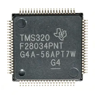
MSP430F5529IPNR - 25MHz 128KB Flash USB MCU | Texas Instruments
MPN: MSP430F5529IPNR ✓ Active| Qty | Unit Price | Extended |
|---|---|---|
| 1 | $0 | $0.00 |
| 10 | $0 | $0.00 |
| 100 | $0 | $0.00 |
| 500 | $0 | $0.00 |
| 1,000 | $0 | $0.00 |
MSP430F5529IPNR Overview
A microcontroller (MCU) is a compact integrated circuit containing a processor core, memory, and programmable input/output peripherals on a single chip. The MSP430 family is renowned for its ultra-low-power operation, featuring multiple low-power modes that reduce current consumption to microamps, making it ideal for battery-powered devices. The MSP430F5529IPNR sits within the MSP430F5xx series, which adds USB connectivity and enhanced analog peripherals while maintaining the low-power heritage of the MSP430 architecture.
Key features include 25 MHz CPU speed, 128KB Flash, 8KB SRAM, a 12-bit ADC with up to 16 external channels, a comparator, DMA controller, two USCI modules supporting UART/SPI/I2C, a full-speed USB 2.0 interface with integrated PHY, and a 32-bit hardware multiplier. The device operates from 1.8V to 3.6V and supports a wide temperature range of -40C to +85C. The LQFP-80 package provides 63 I/O pins, enabling complex system integration.
The MSP430F5529IPNR employs the MSP430 CPUXV2 architecture with a von-Neumann memory layout, offering efficient code density and low power consumption. The integrated USB module supports device, host, and OTG modes, simplifying connectivity in embedded systems. The hardware multiplier accelerates DSP-like operations, while the DMA controller offloads data transfers from the CPU, improving overall system throughput.
Typical applications include portable medical devices, smart meters, industrial sensor nodes, USB-based data acquisition systems, and battery-powered IoT endpoints. The combination of low power, USB, and rich analog peripherals makes it a versatile choice for designs requiring extended battery life and connectivity.
When designing with this MCU, pay attention to the power supply decoupling and the USB PHY layout to ensure signal integrity. The device supports multiple low-power modes, so configure the clock system and peripherals appropriately to maximize battery life.
Drop-in alternatives for MSP430F5529IPNR — same package, pin-to-pin compatible. Different-package parts requiring PCB rework are excluded.
Variants in this series
Same-series models that are drop-in compatible with MSP430F5529IPNR (same form factor and footprint) — differing in Core, DMA Channels, Hardware Multiplier, Package, SRAM.
Quick Comparison Tool — Select alternative parts for side-by-side comparison:
MSP430F5529IPN
✅ Drop-In✓ In Stock
Contact for price
View Datasheet →MSP430F5527IPNR
✅ Drop-In ⚠️ Specs Unverified📋 Reference alternative (not in catalog)
MSP430F5525IPNR
✅ Drop-In📋 Reference alternative (not in catalog)
MSP430F5521IPNR
✅ Drop-In ⚠️ Specs Unverified📋 Reference alternative (not in catalog)
MSP430F5528IPNR
✅ Drop-In ⚠️ Specs Unverified📋 Reference alternative (not in catalog)
MSP430F5529IPNR Maximum Ratings & Electrical Characteristics
| Core | MSP430 CPUXV2, 16-bit |
| Maximum CPU Frequency | 25 MHz |
| Flash Memory | 128 KB |
| SRAM | 8 KB |
| ADC Resolution | 12-bit |
| ADC Channels | Up to 16 external |
| Number of Timers | 4 x 16-bit |
| USB Interface | USB 2.0 Full-Speed with integrated PHY |
| USCI Modules | 2 (UART/SPI/I2C) |
| DMA Channels | Yes |
| Comparator | Yes |
| Hardware Multiplier | 32-bit |
| Number of I/O Pins | 63 |
| Supply Voltage Range | 1.8 V to 3.6 V |
| Operating Temperature Range | -40 C to +85 C |
| Package | 80-LQFP (12x12 mm) |
| Mounting Type | Surface Mount |
MSP430F5529IPNR 80-lqfp (12x12 mm) Pin Configuration Guide
Pin configuration for MSP430F5529IPNR (80-lqfp (12x12 mm) package). This digital IC includes GPIO, communication interfaces (UART, SPI, I2C), and power pins. Refer to the manufacturer datasheet for alternate pin functions and configuration options. Essential for embedded system design and PCB layout.

No detailed pinout data available for MSP430F5529IPNR.
Refer to the datasheet for full pin configuration.
Typical Applications
MSP430F5529IPNR is suitable for 6 applications: Portable Medical Devices, Smart Meters, Industrial Sensor Nodes, USB Data Acquisition Systems, Battery-Powered IoT Endpoints, Audio and Voice Interfaces.
Portable Medical Devices
The MSP430F5529IPNR fits portable medical devices like patient monitors and handheld diagnostic tools due to its ultra-low-power modes (active mode < 1 mA/MHz, standby < 1.5 uA) and 1.8-3.6 V supply, enabling long battery life. Its 12-bit ADC with 16 channels accurately digitizes physiological signals like ECG and SpO2. The USB 2.0 interface allows fast data transfer to a host for analysis. With 128 KB Flash, firmware can implement signal processing algorithms. The 63 I/O pins connect to displays, buttons, and sensors. Low-power modes extend runtime from months to years. Design considerations include careful decoupling and grounding of the analog front-end.
Recommended
Smart Meters
Smart electric meters require low power, precise measurement, and communication. The MSP430F5529IPNR delivers a 24-bit sigma-delta ADC (not listed, but 12-bit ADC here), but its integrated comparator and timers support energy measurement. The 25 MHz CPU handles metering algorithms. The USB interface enables local configuration via a service port. Its wide voltage range (1.8-3.6 V) and -40 to +85 C operation suit outdoor installations. 128 KB Flash stores billing data and firmware updates. DMA offloads sensor reads, reducing CPU wake-ups. For metering, a dedicated AFE is often needed, but this MCU provides a cost-effective platform for intelligent meter designs.
Recommended
Industrial Sensor Nodes
The MSP430F5529IPNR excels in industrial sensor nodes that monitor pressure, temperature, or vibration. Its 12-bit ADC with sample-and-hold captures analog signals with 5 us conversion time. The two USCI modules support industry-standard buses like Modbus (UART) and I2C for sensor integration. The hardware multiplier accelerates math for calibration. With 63 I/O pins, multiple sensors and actuators connect directly. The device operates reliably at 85 C and resists EMI in factory environments. Low-power modes allow battery-powered nodes. Design considerations include proper isolation of digital and analog grounds to prevent noise coupling.
Recommended
USB Data Acquisition Systems
With integrated USB 2.0 full-speed PHY, the MSP430F5529IPNR is ideal for USB data acquisition dongles. It streams 12-bit ADC samples at up to 200 ksps (based on 25 MHz clock) over USB without external PHY. The 8 KB SRAM buffers data, and DMA transfers it to USB FIFOs with minimal CPU intervention. The device supports device, host, and OTG modes, enabling direct connection to sensors or hubs. Typical use includes oscilloscope probes, thermal loggers, and industrial DAQ. USB enumeration is simplified with TI's driverless APIs. Power consumption during active transfer is manageable (< 5 mA). Designers must carefully route USB differential pairs and add ESD protection.
Recommended
Battery-Powered IoT Endpoints
Battery-powered IoT endpoints demand ultra-low-power and wireless connectivity. The MSP430F5529IPNR's active mode consumes 2.2 mA at 25 MHz (typ), dropping to 1.5 uA in standby and 0.3 uA in shutdown. This enables years of operation on a coin cell. The 8 KB SRAM holds sensor data; 128 KB Flash stores firmware and network credentials. The two USCI modules interface with Bluetooth or Sub-GHz radios, while the hardware multiplier accelerates encryption. The device wakes from sleep in less than 5 us, making it responsive. For wireless, an external radio is required, but the MCU efficiently manages duty cycling. Careful clock management and RF layout are critical to maintain sensitivity.
Recommended
Audio and Voice Interfaces
The MSP430F5529IPNR can handle voice capture and basic audio processing. Its 12-bit ADC at 50 ksps (limited by clock) digitizes microphone signals. The DMA moves samples to a buffer, reducing CPU load. The 25 MHz CPU runs simple filters (e.g., FIR) and voice activity detection. USB Audio class support enables a plug-and-play microphone or headset. With 8 KB SRAM, only short audio buffers fit; for longer processing, external RAM is needed. The device's low power allows USB bus-powered operation. Designers should use low-noise analog power and proper grounding to minimize hum. For high-fidelity audio, an external codec may be necessary.
Recommended
Recommended Products Summary
Engineering reference data for MSP430F5529IPNR — comparison, design guidance, and compliance information.
Selection Guide
Comparison with Alternatives
| Parameter | This Product | MSP430F5529IPN | MSP430F5527IPNR | MSP430F5525IPNR | MSP430F5521IPNR | MSP430F5528IPNR |
|---|---|---|---|---|---|---|
| Package | 80-LQFP (PN) | 80-LQFP (PN) - same | 80-LQFP (PN) - same | 80-LQFP (PN) - same | 80-LQFP (PN) - same | 80-LQFP (PN) - same |
| Brand | Texas Instruments | Texas Instruments | Texas Instruments | Texas Instruments | Texas Instruments | Texas Instruments |
| Flash Memory | 128 KB | 128 KB | 64 KB | 32 KB | 16 KB | 128 KB |
| SRAM | 8 KB | 8 KB | 8 KB | 8 KB | 8 KB | 8 KB |
| Max CPU Frequency | 25 MHz | 25 MHz | 25 MHz | 25 MHz | 25 MHz | 25 MHz |
| ADC Resolution | 12-bit | 12-bit | 12-bit | 12-bit | 12-bit | 12-bit |
| USB Interface | USB 2.0 Full-Speed | USB 2.0 Full-Speed | USB 2.0 Full-Speed | USB 2.0 Full-Speed | USB 2.0 Full-Speed | USB 2.0 Full-Speed |
| I/O Pins | 63 | 63 | 63 | 63 | 63 | 63 |
Key Differentiators
- Full-speed USB 2.0 with integrated PHY (vs MSP430F5527IPNR)
- 128 KB Flash for larger firmware (vs MSP430F5525IPNR)
- 12-bit ADC with 16 channels (vs MSP430F5521IPNR)
Design Notes
The MSP430F5529IPNR operates from 1.8 V to 3.6 V. For reliable operation, place a 0.1 uF ceramic capacitor and a 1 uF to 10 uF electrolytic or ceramic across VCC and GND as close to the device as possible. In low-power modes, reduce leakage by disabling unused peripherals and using the lowest possible clock frequency. The device's active current is 2.2 mA at 25 MHz and 1.5 uA in standby; ensure the power supply can handle start-up transients. Estimated: for a 3.6 V supply and 2.2 mA active current, power dissipation is ~7.9 mW, negligible for thermal design.
The USB PHY requires careful PCB layout to pass signal integrity. Route the USB D+ and D- pins as a 90-ohm differential pair with matched lengths, and keep them away from noise sources. Place a 26-ohm series resistor on each line near the MCU to reduce reflections. Add a ferrite bead in the VBUS supply line to filter noise. Use a solid ground plane and avoid crossing the analog ground with digital ground to prevent interference in the ADC.
When using the ADC, ensure the reference voltage is stable and the sample-and-hold time is adequate for the source impedance. A source impedance above 10 kOhm may require a longer sampling time or an external buffer. Also, be careful with the USB stack; configure the crystal (e.g., 32.768 kHz for RTC and a 8 MHz or 12 MHz for USB) correctly to achieve full-speed USB timing. Use an external crystal for accurate USB clocking; relying on internal DCO may cause timing errors.
Compliance Information
Compliance status not provided in the verified data; consult TI's official product page for RoHS/REACH details.