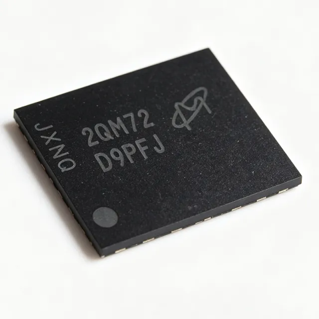
MT41K256M8DA-125 - 2Gb DDR3L SDRAM x8 800MHz | Micron
MPN: MT41K256M8DA-125 ✓ Active| Qty | Unit Price | Extended |
|---|---|---|
| 1 | $4.2 | $4.20 |
| 10 | $3.9 | $39.00 |
| 100 | $3.45 | $345.00 |
| 500 | $3.1 | $1,550.00 |
| 1,000 | $2.85 | $2,850.00 |
MT41K256M8DA-125 Overview
DDR3L SDRAM is a low-voltage version of the JEDEC-standard DDR3 SDRAM. DDR3 doubles the data rate of DDR2 by using an 8-bit prefetch architecture and fly-by-terminated signal routing, while DDR3L further reduces core power by operating at 1.35V instead of 1.5V. It is also backward compatible with 1.5V DDR3 operation per Micron documentation. DRAM components like this device form the main-memory tier of the memory hierarchy, sitting between CPU caches and storage, and are managed by a DDR memory controller on the host processor or chipset.
Key features include 8 internal banks, programmable CAS latency, two fixed burst lengths (BL8 and BC4 via mode register or on-the-fly), auto self-refresh and auto precharge, an asynchronous reset pin for fast initialization, data mask (TDQS/DM) support, dynamic on-die termination (ODT), ZQ output driver calibration, and write leveling for fly-by topology signal integrity.
Technically, the device uses an 8n-bit prefetch architecture with a SSTL-15 compatible I/O interface (1.35V nominal) and supports derated timing at elevated temperature. The -125 speed grade corresponds to 13.75 ns CL=11 timing at 800 MT/s. The industrial-grade IT variant extends operation to -40C to +95C.
Typical applications include embedded systems main memory, industrial PCs, networking equipment, set-top boxes, and test instrumentation requiring compact, low-power DRAM in a space-saving FBGA footprint.
Design consideration: DDR3L fly-by routing requires per-device write leveling in the memory controller; verify ODT settings and ZQ calibration resistor placement per the Micron datasheet layout guidelines.
This page synthesizes distributor pricing, drop-in alternatives, and practical design notes not found in the manufacturer datasheet.
Drop-in alternatives for MT41K256M8DA-125 — same package, pin-to-pin compatible. Different-package parts requiring PCB rework are excluded.
Variants in this series
Same-series models that are drop-in compatible with MT41K256M8DA-125 (same form factor and footprint) — differing in Burst Length, CAS Latency, Clock Frequency, Data Rate, Memory Size.
Quick Comparison Tool — Select alternative parts for side-by-side comparison:
MT41K256M8DA-125 IT:K
📋 Reference alternative (not in catalog)
MT41K256M8DA-125 AIT:K TR
📋 Reference alternative (not in catalog)
MT41K256M8DA-125:M
📋 Reference alternative (not in catalog)
MT41K256M8DA-125 Specifications
| Memory Type | DDR3L SDRAM |
| Memory Size | 2 Gbit |
| Organization | 256M x 8 |
| Interface | Parallel |
| Data Rate | 800 MT/s |
| Clock Frequency | 400 MHz |
| Access Time (CL=11) | 13.75 ns |
| Supply Voltage | 1.35 V (1.5 V DDR3 compatible mode) |
| Internal Banks | 8 |
| CAS Latency | Programmable (CL=11 at -125 speed grade) |
| Burst Length | 8 (BL8) or 4 (BC4), fixed via MRS or on-the-fly |
| Features | Auto self-refresh, auto precharge, asynchronous reset, data mask, dynamic ODT, ZQ calibration, write leveling |
| Operating Temperature (standard) | 0C to +85C (commercial K suffix) |
| Operating Temperature (IT variant) | -40C to +95C |
| Package | 78-FBGA (8 mm x 10.5 mm) |
| Mounting Type | Surface Mount |
MT41K256M8DA-125 78-fbga (8 mm x 10.5 mm) Pin Configuration Guide
Pin configuration for MT41K256M8DA-125 (78-fbga (8 mm x 10.5 mm) package). Pin numbering, functions, and connection diagrams are defined in the manufacturer datasheet. Refer to it for the exact footprint and soldering guidelines.

No detailed pinout data available for MT41K256M8DA-125.
Refer to the datasheet for full pin configuration.
Typical Applications
MT41K256M8DA-125 is suitable for 6 applications: Embedded Systems Main Memory, Industrial PCs and HMIs, Networking Equipment, Set-Top Boxes and Consumer Multimedia, Test and Measurement Instrumentation, Medical Diagnostic Equipment.
Embedded Systems Main Memory
The MT41K256M8DA-125 provides 2Gb of main memory for embedded processors and SoCs with DDR3L controllers. Its 256M x 8 organization matches single-channel x8 memory interfaces on ARM and x86 embedded SoCs, and the 800 MT/s speed grade provides 1.6 GB/s of peak bandwidth per device, sufficient for RTOS and Linux-based embedded applications. The 1.35V supply cuts memory-subsystem power roughly 20-25% versus 1.5V DDR3, an important figure for fanless industrial controllers. Dynamic ODT and write leveling ensure signal integrity on fly-by-routed boards, while the asynchronous RESET# pin allows fast re-initialization after system resets.
Recommended
Industrial PCs and HMIs
Industrial PCs, panel HMIs, and edge gateways operate in uncontrolled environments, making the MT41K256M8DA-125 IT:K industrial variant (-40C to +95C) a strong fit for their main memory. The 2Gb density supports 1-2 GB system RAM configurations typical of fanless IPCs, and auto self-refresh maintains data integrity during low-power standby states required by energy-saving modes. The 78-FBGA (8 x 10.5 mm) footprint keeps the memory section compact on dense carrier boards. Micron's IT-grade screening supports the long service lives (5-10 years) expected in factory automation and building control deployments.
Recommended
Networking Equipment
Routers, switches, and network-attached processing platforms use the MT41K256M8DA-125 as control-plane memory for packet buffers, routing tables, and management software. The 800 MT/s rate at CL=11 (13.75 ns) delivers responsive control-plane performance, while the 1.35V operation reduces power in always-on telecom infrastructure where thermal budget and energy cost matter. Write leveling supports the fly-by clock routing typical of multi-drop DDR3 topologies on network processor reference boards, and ZQ calibration maintains drive strength over temperature and process variation, keeping timing margins stable in high-ambient equipment racks.
Recommended
Set-Top Boxes and Consumer Multimedia
Set-top boxes, IPTV receivers, and smart-media platforms use the MT41K256M8DA-125 for video buffering and application memory. The 2Gb x8 configuration pairs naturally with cost-sensitive SoCs that expose one x8 DDR3L channel, and the 800 MT/s bandwidth sustains 1080p video decode buffering requirements. The 1.35V rail simplifies integration with the low-voltage PMIC rails common in consumer designs, and the compact 78-FBGA package fits the tight board areas of streaming-media form factors. Commercial-grade :K temperature rating (0C to +85C) covers typical indoor consumer operating conditions economically.
Recommended
Test and Measurement Instrumentation
Oscilloscopes, logic analyzers, and data-acquisition instruments use the MT41K256M8DA-125 as acquisition-buffer and application memory. The 1.6 GB/s peak bandwidth per device supports deep waveform capture buffering, and DDR3L operation reduces instrument internal heat rise, protecting calibration stability in sealed enclosures. Micron's published AC timing tables for the -125 speed grade allow deterministic memory-controller design, and the asynchronous RESET# input supports clean recovery after instrument power events. Instrument designs with wide environmental specs should select the IT variant rated -40C to +95C.
Recommended
Medical Diagnostic Equipment
Patient monitors, diagnostic analyzers, and imaging front-ends deploy the MT41K256M8DA-125 as working memory for sensor data processing. The IT temperature variant supports the -40C to +95C range required by storage and transport conditions of portable medical devices, while dynamic ODT and write leveling preserve memory-interface margins critical to long-term data integrity in life-safety equipment. Low 1.35V operation reduces battery drain in ambulatory monitors. The 2Gb density balances cost against the moderate RAM footprints (0.5-2 GB) typical of embedded medical application processors.
Recommended
Recommended Products Summary
Engineering reference data for MT41K256M8DA-125 — comparison, design guidance, and compliance information.
Selection Guide
Comparison with Alternatives
| Parameter | This Product | MT41K256M8DA-125 IT | MT41K256M8DA-125 AIT | MT41K256M8DA-125 |
|---|---|---|---|---|
| Package | 78-FBGA (8x10.5) | K: 78-FBGA (8x10.5) - same | K TR: 78-FBGA (8x10.5) - same | M: 78-FBGA (8x10.5) - same |
| Brand | Micron Technology | K: Micron Technology | K TR: Micron Technology | M: Micron Technology |
| Memory Size / Organization | 2 Gbit, 256M x 8 | K: 2 Gbit, 256M x 8 | K TR: 2 Gbit, 256M x 8 | M: 2 Gbit, 256M x 8 |
| Data Rate | 800 MT/s | K: 800 MT/s | K TR: 800 MT/s | M: 800 MT/s |
| Supply Voltage | 1.35 V (DDR3L) | K: 1.35 V (DDR3L) | K TR: 1.35 V (DDR3L) | M: 1.35 V (DDR3L) |
| Access Time (CL=11) | 13.75 ns | K: 13.75 ns | K TR: 13.75 ns | M: 13.75 ns |
| Key Features | Auto self-refresh, dynamic ODT, ZQ cal, write leveling, async reset | K: Same feature set (per LCSC listing) | K TR: Same die, extended screening | M: Same electrical feature set |
Key Differentiators
- Extended industrial temperature option (vs MT41K256M8DA-125 (commercial :K, this part's own grade baseline))
- Moderate speed grade cost advantage (vs MT41K256M8DA-125:M)
- Full DDR3L feature set at 2Gb density (vs MT41K256M8DA-125 AIT:K TR)
Design Notes
DDR3L fly-by routing requires write leveling at the memory controller; enable WL training in the controller boot sequence and verify per-byte DQS gate timing. Use dynamic ODT during writes to reduce reflections, and place the ZQ calibration resistor (240 ohm, 1%) within 25 mm of the ZQ ball with a direct low-inductance ground return. Follow Micron's DDR3 point-to-point design guide for trace length matching (CK to address within ±25 mils) and reference-plane continuity under all address/command traces.
The 1.35V VDD/VDDQ rails should each be decoupled with multiple 0.1uF and 10uF ceramics placed across the FBGA ball field. Estimated: at 800 MT/s with ~50% read activity, a single 2Gb device draws roughly 150-300 mA, so size the VDDQ rail budget accordingly; do not present this estimate as a datasheet figure. The 1.5V-compatible mode should only be used after confirming your controller's voltage-derating behavior per the Micron datasheet note referring DDR3L operation back to the 1.5V DDR3 data sheet.
Do not confuse speed-grade suffixes: -125 denotes CL=11 at 800 MT/s (13.75 ns), not a 125 MHz part. Also distinguish :K from :M and IT suffixes when generating POs, since ordering errors between commercial and industrial grades are a frequent sourcing mistake. Tie RESET# through an RC or supervisor output, never leave it floating - an un-controlled reset during power ramp can leave the DRAM in an undefined state and corrupt training results.
Compliance Information
Compliance status not explicitly stated in the provided verified data; consult the Micron product page for current RoHS/REACH declarations.


