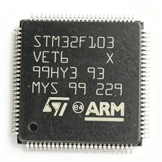
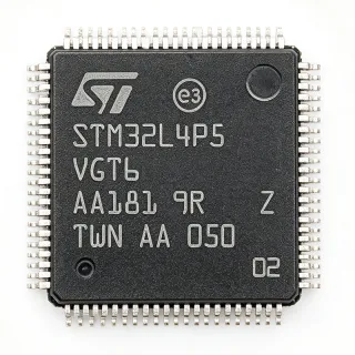
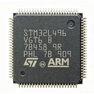
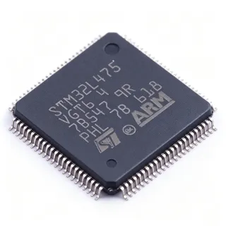
STM32F103V8T6 - ARM Cortex-M3 72MHz MCU 64KB Flash | ST
MPN: STM32F103V8T6 ✓ Active| Qty | Unit Price | Extended |
|---|---|---|
| 1 | $5.91 | $5.91 |
| 10 | $5.55 | $55.50 |
| 100 | $5.1 | $510.00 |
| 500 | $4.75 | $2,375.00 |
| 1,000 | $4.4 | $4,400.00 |
STM32F103V8T6 Overview
A microcontroller (MCU) integrates a processor core, memory, and peripherals onto a single chip, forming the lowest layer of the embedded computing hierarchy below microprocessors and application processors. The STM32F1 Performance line belongs to ST's STM32 family of general-purpose MCUs, based on the ARM Cortex-M3 32-bit RISC core.
Key features of the STM32F103V8T6 include the 72 MHz Cortex-M3 core, 64 KB on-chip Flash and 20 KB SRAM, two 12-bit ADCs, a USB 2.0 full-speed interface, a CAN 2.0B controller, and seven 16-bit timers per ST's official product description.
The Cortex-M3 Harvard architecture delivers deterministic interrupt handling through the Nested Vectored Interrupt Controller, while the embedded Flash with prefetch buffer sustains full-speed core operation. The peripheral set spans multiple USART, SPI, and I2C interfaces, enabling rich connectivity within a single supply domain.
Typical applications include industrial control boards, motor-control nodes, communication modules, and low-cost embedded platforms - markets where the STM32F103 line has been a default choice for over fifteen years.
Designers should verify Flash wait-state configuration at 72 MHz (two wait states) and confirm second-source compatibility for clock and HAL settings when using drop-in substitutes.
This page synthesizes distributor pricing, validated drop-in alternatives, and cross-reference guidance not found in the manufacturer datasheet, with pricing verified as of 2026-09-06.
Drop-in alternatives for STM32F103V8T6 — same package, pin-to-pin compatible. Different-package parts requiring PCB rework are excluded.
Variants in this series
Same-series models that are drop-in compatible with STM32F103V8T6 (same form factor and footprint) — differing in CAN, Core, Flash Memory, Package, SRAM.
Quick Comparison Tool — Select alternative parts for side-by-side comparison:
No drop-in alternatives available for this product.
Request AlternativesSTM32F103V8T6 Maximum Ratings & Electrical Characteristics
| Core | ARM Cortex-M3 32-bit |
| Core Frequency | 72 MHz |
| Flash Memory | 64 KB (64K x 8) |
| SRAM | 20 KB |
| ADC Resolution | 12-bit x 2 |
| Timers | Seven 16-bit timers |
| USB | USB 2.0 full-speed |
| CAN | CAN 2.0B |
| Package | 100-LQFP (14x14 mm) |
| Mounting Type | Surface Mount |
| Product Line | STM32F1 Performance line |
| Data Bus Width | 32 bit |
| Communication Interfaces | USB, CAN, USART, SPI, I2C |
STM32F103V8T6 100-lqfp (14x14 mm) Pin Configuration Guide
Pin configuration for STM32F103V8T6 (100-lqfp (14x14 mm) package). This digital IC includes GPIO, communication interfaces (UART, SPI, I2C), and power pins. Refer to the manufacturer datasheet for alternate pin functions and configuration options. Essential for embedded system design and PCB layout.

No detailed pinout data available for STM32F103V8T6.
Refer to the datasheet for full pin configuration.
Typical Applications
STM32F103V8T6 is suitable for 6 applications: Industrial Control Boards, Motor Control Nodes, Communication and Networking Modules, USB Peripheral Devices, Low-Cost Development Platforms, Medical and Diagnostic Instrumentation.
Industrial Control Boards
The STM32F103V8T6 fits industrial control boards through its 72 MHz Cortex-M3 core, seven 16-bit timers, and rich GPIO count (up to 80 I/Os on the 100-pin LQFP), enabling relay sequencing, sensor polling, and HMI interfacing from one chip. Its USB and CAN interfaces bridge factory-field buses to higher-level systems, while the two 12-bit ADCs handle analog setpoint and feedback channels. The STM32F103 architecture is widely used in PLC I/O modules and process-control nodes because of its deterministic interrupt latency and mature ST ecosystem. Designers should budget Flash carefully at 64 KB, using the STM32F103VBT6 (128 KB, same footprint) when protocol stacks grow.
Recommended
Motor Control Nodes
For motor control, the STM32F103V8T6 provides the advanced 16-bit timers with complementary PWM outputs and dead-time insertion required to drive three-phase inverters for BLDC and PMSM motors. The two 12-bit ADCs support simultaneous current-sense sampling for field-oriented control loops, and the 72 MHz core executes the control mathematics within typical PWM periods. ST's STM32F1 line has long served industrial drives and low-cost servo nodes for exactly this peripheral combination. Engineers should route current-shunt signals to ADC channels with minimal trace length and use the timer break input for hardware fault shutdown, ensuring safe inverter behavior during overcurrent events.
Recommended
Communication and Networking Modules
The STM32F103V8T6 serves communication modules because it uniquely combines USB 2.0 full-speed device, CAN 2.0B, and multiple USART/SPI/I2C interfaces on one chip. Typical uses include USB-to-CAN bridges, RS485/Modbus gateways, and sensor concentrators where data must move between field buses and host systems. The 20 KB SRAM buffers packet streams, and the 64 KB Flash stores protocol stacks with room for a small boot loader. When porting firmware to the pin-compatible GD32F103V8T6 second source, designers must recheck clock configuration and Flash wait-state settings, since the substitute core runs up to 108 MHz and timing-sensitive UART baud generators may need recalibration.
Recommended
USB Peripheral Devices
With its integrated USB 2.0 full-speed device controller, the STM32F103V8T6 implements USB HID, CDC virtual COM port, and custom bulk-device class products without an external USB chip. The 100-pin LQFP provides enough GPIO for keyboards, data loggers, and instrumentation panels alongside the USB interface, while the 12-bit ADCs digitize analog inputs locally. ST's USB device library for the STM32F1 line is mature, shortening development cycles for certified USB endpoints. Designers must provide the 1.5 kOhm pull-up on D+ (or enable the internal pull-up depending on board revision) and a stable 48 MHz USB clock derived from the PLL, so crystal selection and PLL multiplier settings must be verified at design time.
Recommended
Low-Cost Development Platforms
The STM32F103V8T6 is a mainstay of low-cost development platforms and evaluation boards, including STM32-family boards and third-party 100-pin F103 designs, because of its approachable Cortex-M3 architecture and the extensive ST ecosystem (standard peripheral library, HAL, RTOS ports, and debug support via SWD and JTAG). Universities, hobbyists, and product prototypes benefit from the enormous body of community code targeting the F103. The 100-pin LQFP exposes all buses for experimentation. When sourcing boards in 2026, be aware that STM32F103 lead times have stretched past 26 weeks for some combinations, so platform vendors increasingly pair the original with validated GD32F103 pin-compatible substitutes on the same footprint.
Recommended
Medical and Diagnostic Instrumentation
Non-life-critical medical instrumentation - patient-data terminals, portable diagnostic readers, and lab measurement nodes - uses the STM32F103V8T6 for its quiet 12-bit ADC performance, USB connectivity for data export, and long-term component familiarity among regulated-design teams. The 72 MHz core handles filtering and user-interface tasks, while the CAN interface links modules inside larger analyzers. Its commercial temperature rating suits benchtop equipment; battery-portable instruments must account for the F103 power profile in sleep and stop modes when sizing cells. Because 64 KB Flash constrains firmware for display-plus-protocol duties, teams often specify the pin-compatible STM32F103VBT6 with 128 KB to leave headroom for future certified firmware revisions.
Recommended
Recommended Products Summary
Engineering reference data for STM32F103V8T6 — comparison, design guidance, and compliance information.
Selection Guide
Comparison with Alternatives
| Parameter | This Product | STM32F103VBT6 | STM32F103VCT6 | GD32F103V8T6 | APM32F103V8T6 |
|---|---|---|---|---|---|
| Package | 100-LQFP (14x14 mm) | 100-LQFP (14x14 mm) - same | 100-LQFP (14x14 mm) - same | 100-LQFP (14x14 mm) - same | 100-LQFP (14x14 mm) - same |
| Brand | STMicroelectronics | STMicroelectronics | STMicroelectronics | GigaDevice | Geehy Semiconductor |
| Core / Frequency | ARM Cortex-M3 @ 72 MHz | Cortex-M3 @ 72 MHz | Cortex-M3 @ 72 MHz | Cortex-M3 @ up to 108 MHz | Cortex-M3 @ 72 MHz class |
| Flash | 64 KB | 128 KB | 256 KB | 64 KB | 64 KB |
| SRAM | 20 KB | 20 KB | 48 KB | 20 KB | 20 KB |
| ADC | 2x 12-bit | 2x 12-bit | 2x 12-bit | 2x 12-bit | 2x 12-bit |
| USB / CAN | USB FS / CAN 2.0B | USB FS / CAN 2.0B | USB FS / CAN 2.0B | USB FS / CAN 2.0B | USB FS / CAN 2.0B |
| Software Compatibility | Native ST ecosystem (HAL, StdPeriph, STM32Cube) | Native ST ecosystem - identical | Native ST ecosystem - identical | Largely register-compatible; recheck clock/wait-states/HAL | STM32-compatible; verify peripheral timing |
Key Differentiators
- Native ST ecosystem and documentation depth (vs GD32F103V8T6)
- Cost-down and supply-security via validated second sources (vs STM32F103VBT6)
- Memory scalability without PCB change (vs STM32F103VCT6)
Design Notes
Flash wait states: the STM32F103V8T6 requires two CPU wait states when running from embedded Flash at 72 MHz (0-24 MHz: 0 WS; 24-48 MHz: 1 WS; 48-72 MHz: 2 WS). Omitting this configuration in the option/flash registers causes hard faults or corrupted execution at full speed. When porting firmware to the GD32F103V8T6 second source, recheck wait-state and clock-tree settings because the substitute core runs up to 108 MHz and Flash acceleration differs - per JLink Technology's cross-reference guidance, 'recheck clock, Flash wait-states, and some HAL settings when porting'.
Place a 100 nF ceramic decoupling capacitor at each VDD/VSS pin pair of the 100-pin LQFP plus one bulk 4.7-10 uF capacitor per supply domain, keeping VDDA/VSSA on a separate filtered analog supply (ferrite bead plus 1 uF + 10 nF) to preserve 12-bit ADC accuracy. The 14x14 mm LQFP-100 has 0.5 mm pitch; use NSMD pads and inspect with 10x minimum during reflow qualification. Route USB D+/D- as a 90-ohm differential pair matched within 0.15 mm when using the full-speed interface.
Second-source validation: Senneon's cross-reference explicitly states P2P does not guarantee drop-in - engineers 'must still review the disclosed differences, datasheets and application conditions before production use.' For GD32F103V8T6, quantified review points are core clock (108 MHz max vs 72 MHz), Flash zero-wait-state execution behavior, and power-consumption deltas in sleep modes, which affect battery-powered BOMs. Qualify at temperature extremes with your actual firmware image, including analog peripherals, before approving the alternate for production builds.
Compliance Information
RoHS/lead-free inferred from ST's current-production STM32 portfolio and T6 package suffix; obtain the official ST environmental declaration for certification packages. AEC-Q100 not claimed for the commercial STM32F103V8T6.