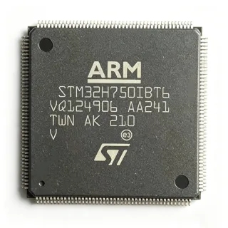
STM32F769IGT6 - 216MHz Cortex-M7 MCU, 1MB Flash | STMicroelectronics
MPN: STM32F769IGT6 ✓ Active| Qty | Unit Price | Extended |
|---|---|---|
| 1 | $22.5 | $22.50 |
| 10 | $20.4 | $204.00 |
| 100 | $17.8 | $1,780.00 |
| 500 | $15.95 | $7,975.00 |
| 1,000 | $14.1 | $14,100.00 |
STM32F769IGT6 Overview
What is a Cortex-M7 microcontroller? The Cortex-M7 is Arm's highest-performance microcontroller core for embedded applications, designed for real-time control and DSP. It sits in the hierarchy as: Cortex-M7 -> ARM Cortex-M family -> 32-bit MCU -> microcontroller -> semiconductor. The STM32F7 series integrates this core with large SRAM, hardware graphics (Chrom-ART accelerator, JPEG codec), and rich connectivity, making it suitable for high-end HMI, audio, and motor control.
Key features of the STM32F769IGT6 include: 1 MB Flash with dual-bank architecture for live firmware upgrades, up to 2 MB external memory expansion via FMC (Flexible Memory Controller), 16-bit ADCs (up to 3 MSPS), two CAN 2.0B interfaces, USB OTG full-speed + USB OTG high-speed with on-chip HS PHY, two SDMMC interfaces, TFT-LCD controller, and the Chrom-ART graphics accelerator. The 176-LQFP exposes the maximum peripheral set of the F7 series, including 8-bit/16-bit FSMC, SAI audio interfaces, and SPDIF-Rx.
Architecturally, the STM32F769IGT6 uses an advanced 90 nm process with an adaptive real-time ART Accelerator that delivers zero-wait-state execution from Flash at full 216 MHz. Multi-layer AHB/APB bus matrix, 16 DMA streams with FIFOs, and a dedicated DMA2D engine for image data transfer accelerate data movement. The MCU operates at 1.7-3.6 V with selectable LDO/SMPS regulator (BYPASS_REG pin) and includes a real-time clock, watchdog, and SysTick.
Primary applications are high-end human-machine interface (HMI) panels, smart-home gateways, motor drives, professional audio, point-of-sale terminals, and embedded graphics with TFT-LCD + touch. The integrated TFT-LCD controller and JPEG codec remove the need for an external graphics MCU in many designs.
Design consideration: the LQFP-176 package is large (24x24 mm) and requires careful PCB layout for the high-speed USB HS, SDMMC, and external memory interfaces. Use impedance-controlled traces for USB and RMII, and isolate analog/digital grounds.
This page synthesizes distributor pricing, drop-in same-package alternatives (STM32F767IIT6 with 2 MB Flash, STM32F765IGT6), and practical design notes not found in the manufacturer datasheet alone.
Drop-in alternatives for STM32F769IGT6 — same package, pin-to-pin compatible. Different-package parts requiring PCB rework are excluded.
Variants in this series
Same-series models that are drop-in compatible with STM32F769IGT6 (same form factor and footprint) — differing in SRAM, ADC, Package, Core, Flash Memory.
Quick Comparison Tool — Select alternative parts for side-by-side comparison:
STM32F767IIT6
✅ Drop-In✓ In Stock
$11.95 / Unit
View Datasheet →STM32F765IGT6
✅ Drop-In✓ In Stock
$13.1 / Unit
View Datasheet →STM32F746IGT6
✅ Drop-In✓ In Stock
$13.76 / Unit
View Datasheet →STM32F769IGT6 Maximum Ratings & Electrical Characteristics
| Core | ARM Cortex-M7 with FPU + DSP |
| Maximum Clock Frequency | 216 MHz |
| DMIPS | 462 |
| Flash Memory | 1 MB |
| SRAM | 340 KB + 16 KB (D2 SRAM) |
| Operating Voltage | 1.7 V to 3.6 V |
| Package | 176-LQFP (24x24 mm) |
| Supply Scheme | LDO / SMPS selectable via BYPASS_REG pin |
| Number of I/Os | Up to 140 GPIO |
| ADC | 3x 12-bit, up to 2.4 MSPS |
| DAC | 2x 12-bit |
| USB | USB OTG FS + USB OTG HS (on-chip HS PHY) |
| CAN | 2x CAN 2.0B |
| SDMMC | 2x SDMMC |
| Display Controller | TFT-LCD, Chrom-ART accelerator, JPEG codec |
| External Memory Bus | FMC, supports SRAM/PSRAM/NOR/NAND/SDRAM |
| Operating Temperature | -40C to +85C (industrial) |
| RoHS Status | Compliant |
| Mounting Type | Surface Mount |
STM32F769IGT6 176-lqfp (24x24 mm) Pin Configuration Guide
Pin configuration for STM32F769IGT6 (176-lqfp (24x24 mm) package). This digital IC includes GPIO, communication interfaces (UART, SPI, I2C), and power pins. Refer to the manufacturer datasheet for alternate pin functions and configuration options. Essential for embedded system design and PCB layout.

No detailed pinout data available for STM32F769IGT6.
Refer to the datasheet for full pin configuration.
Typical Applications
STM32F769IGT6 is suitable for 6 applications: High-End Human-Machine Interface (HMI), Industrial Motor Control, Professional Audio Processing, Smart Home Gateway & IoT Hub, Point-of-Sale (POS) Terminal, Embedded Graphics with TFT-LCD Display.
High-End Human-Machine Interface (HMI)
The STM32F769IGT6 is purpose-built for premium HMI panels. Its integrated TFT-LCD controller supports 24-bit color displays up to WVGA resolution without external graphics ICs, reducing BOM cost. The Chrom-ART accelerator accelerates 2D operations (blits, fills, pixel format conversions), and the hardware JPEG decoder/encoder offloads image compression. With 340 KB SRAM, full HMI screens with animated widgets can reside on-chip. The Cortex-M7 at 216 MHz drives real-time touch response and UI logic. Pair with an external SDRAM via FMC for large image assets. The LQFP-176 footprint is widely adopted in industrial HMI modules, easing redesign.
Recommended
Industrial Motor Control
The STM32F769IGT6 is suited for 3-phase motor drives (PMSM, BLDC, ACIM) thanks to its Cortex-M7 DSP extensions, 216 MHz core, and dual 12-bit ADCs with synchronized sampling. Two advanced timers (TIM1, TIM8) generate complementary PWM with dead-time insertion and hardware break, while HRTIM (high-resolution timer, 217 ps resolution) drives digital power conversion. The 340 KB SRAM enables field-oriented control loops at sub-microsecond step times. CAN 2.0B and UART/USART enable industrial networking (CANopen, Modbus). The 1.7-3.6 V range and -40 to +85C industrial grade suit harsh factory environments.
Recommended
Professional Audio Processing
The STM32F769IGT6 is ideal for professional audio products: the Cortex-M7 with DSP extensions executes EQ, compression, FIR filters, and FFT at audio rates, while SAI and SPDIF-Rx interfaces connect to high-end DACs and ADCs (such as the WM8741). The 340 KB SRAM accommodates large audio buffers; 1 MB Flash stores presets and DSP coefficients. The integrated SAI supports I2S, LJ, RJ, TDM protocols up to 192 kHz on multiple channels. USB OTG HS enables 24-bit/192 kHz USB Audio Class 2 streaming to hosts. DMA with FIFO decouples audio I/O from CPU.
Recommended
Smart Home Gateway & IoT Hub
The STM32F769IGT6 functions as a smart-home or industrial IoT gateway controller. Dual SDMMC interfaces allow eMMC storage plus SD card support for local data logging. Ethernet MAC plus USB OTG HS enable simultaneous wired and wireless dongle connections. The TFT-LCD + touch controller drives the on-device display, removing the need for a separate HMI MCU. With 1 MB Flash and 340 KB SRAM, the part can run TCP/IP, TLS, and an MQTT/CoAP stack alongside application logic. The 1.7-3.6 V range supports coin-cell backup of RTC for time synchronization.
Recommended
Point-of-Sale (POS) Terminal
The STM32F769IGT6 anchors a compact POS terminal with built-in customer-facing display. The TFT-LCD controller drives the merchant display, the touchscreen interface uses the SAI or simple GPIO for capacitive touch, and the USB OTG HS handles printer and peripheral connectivity. SDMMC drives a microSD card for transaction logging, while the 1 MB Flash stores firmware and localized UI assets. Hardware AES-256 (in some STM32F7 variants via crypto module) and True RNG support secure transactions. Two CAN 2.0B ports can interface with back-office equipment.
Recommended
Embedded Graphics with TFT-LCD Display
The STM32F769IGT6 drives TFT-LCD panels directly via its integrated LTDC controller supporting up to 24-bit color, and accelerates rendering via the Chrom-ART DMA2D engine. The hardware JPEG codec decodes camera or image assets without CPU overhead, while the MIPI-DSI interface (available on some F769 package variants) drives modern smartphone-style displays. With 216 MHz Cortex-M7 and 340 KB SRAM, mid-resolution HMI runs smoothly. The LQFP-176 footprint exposes the full parallel RGB interface plus all the FMC/SDMMC needed for SDRAM and storage, eliminating external controllers.
Recommended
Recommended Products Summary
Engineering reference data for STM32F769IGT6 — comparison, design guidance, and compliance information.
Selection Guide
Comparison with Alternatives
| Parameter | This Product | STM32F767IIT6 | STM32F765IGT6 | STM32F746IGT6 |
|---|---|---|---|---|
| Brand | STMicroelectronics | STMicroelectronics | STMicroelectronics | STMicroelectronics |
| Package | 176-LQFP (24x24 mm) | 176-LQFP (24x24 mm) - same | 176-LQFP (24x24 mm) - same | 176-LQFP (24x24 mm) - same |
| Core | Cortex-M7 + FPU + DSP | Cortex-M7 + FPU + DSP | Cortex-M7 + FPU + DSP | Cortex-M7 + FPU + DSP |
| Maximum Clock | 216 MHz | 216 MHz | 216 MHz | 216 MHz |
| Flash | 1 MB | 2 MB | 1 MB | 1 MB |
| SRAM | 340 + 16 KB | 512 + 16 KB | 340 + 16 KB | 320 + 16 KB |
| TFT-LCD Controller | Yes (24-bit) | Yes (24-bit) | Yes (24-bit) | Yes (24-bit) |
| MIPI-DSI | Yes | No | No | No |
| JPEG Codec | Yes (HW) | Yes (HW) | No | No |
| USB OTG HS PHY | Yes (on-chip) | Yes (on-chip) | Yes (on-chip) | Yes (on-chip) |
Key Differentiators
- Integrated MIPI-DSI display interface (vs STM32F767IIT6)
- Hardware JPEG codec on-chip (vs STM32F765IGT6)
- Lower cost than F767 with 2 MB Flash (vs STM32F767IIT6)
- Industrial-grade temperature range (vs STM32F746IGT6)
Design Notes
The STM32F769IGT6 supports both LDO and SMPS supply modes. When using the internal SMPS (BYPASS_REG pin left floating or driven low), place a 4.7 uF + 100 nF cap close to VDDSMPS pins. For noise-sensitive analog designs, select LDO mode (BYPASS_REG pin tied to VDD) to avoid SMPS switching ripple. Ensure VDDA/VREF+ have separate low-noise filtering (10 ohm + 100 nF + 1 uF). The PDR_ON pin enables power-down reset; tie to VDD for active reset.
The LQFP-176 package has a 0.5 mm pitch and requires careful PCB routing. For high-speed USB OTG HS (480 Mbps), keep D+/D- traces 90-mimpedance-controlled, length-matched within 2 mm, and shielded with a ground pour. The SDMMC and FMC signals to external SDRAM should be length-matched within 5 mm and routed over a continuous ground plane. Use 4-layer PCB minimum with dedicated ground and power planes; isolate analog/digital grounds at the AGND pin.
Decouple every VDD pin with a 100 nF X7R ceramic placed within 3 mm of the pin. Add 4.7 uF bulk caps on each VDD domain (VDD, VDDA). The HSE crystal oscillator (typically 8 MHz or 16 MHz) traces must be short and surrounded by ground; the LSE 32.768 kHz crystal traces must be kept short and away from switching signals to avoid RTC drift. Place the BOOT0 pin accessible via test pad or jumper for firmware recovery.
Common pitfalls: (1) Forgetting the BYPASS_REG pin state - tying it high disables the internal SMPS and requires external 1.0 V supply. (2) Using HSE without proper load capacitors matching the crystal CL value (typically 8-20 pF). (3) Enabling the USB OTG HS PHY without the 48 MHz clock source - HS PHY needs HSE or HSI48 with CRS. (4) Exceeding the FMC SDRAM timing budget by routing address/data signals too long. (5) Forgetting to set the I/O speed register (OSPEEDR) to high-speed for high-bandwidth SDMMC and parallel RGB interfaces.
For parallel RGB TFT-LCD at high pixel clock (>30 MHz), use controlled-impedance routing (typically 50 ohm single-ended) and series-terminate the clock and sync signals. The SDRAM connected to FMC benefits from matched-length traces for CLK, DQS, and data/address. The SDMMC signals to eMMC should be routed as 50 ohm differential pairs with ground reference; avoid vias on these signals. If using MIPI-DSI, follow the high-speed PCB layout rules strictly (matched length, no stubs).
Compliance Information
RoHS compliant per ST product page. Industrial grade -40 to +85C. Not AEC-Q100 qualified (not automotive). The STM32F769AIHT6 variant is AEC-Q100 qualified.