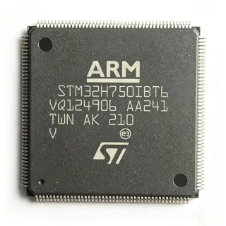
STM32H743IIT6 - 480MHz Cortex-M7 MCU 2MB Flash | ST
MPN: STM32H743IIT6 ✓ Active| Qty | Unit Price | Extended |
|---|---|---|
| 1 | $12.5 | $12.50 |
| 10 | $11.4 | $114.00 |
| 100 | $10.2 | $1,020.00 |
| 500 | $9.6 | $4,800.00 |
| 1,000 | $8.9 | $8,900.00 |
STM32H743IIT6 Overview
A microcontroller (MCU) is a single-chip computer that integrates a processor core, memory, and programmable peripherals on one die. Within the semiconductor hierarchy, the STM32H743IIT6 belongs to the STM32H7 family of high-performance MCUs, which sits above general-purpose lines such as STM32F4/F7 in ST's portfolio and serves as the processing heart of embedded systems where heavy computation, rich connectivity, and real-time control must coexist.
Key features include the Cortex-M7 core with 16 KB instruction and 16 KB L1 data caches, delivering up to 1027 DMIPS (2.14 DMIPS/MHz per Dhrystone 2.1), the ART Accelerator for zero-wait-state execution from Flash, and an external memory interface (FMC/QUADSPI) for expansion. Peripherals span Ethernet, USB, CAN, and multiple UART/SPI/I2C ports, with roughly 140 GPIO pins available in the LQFP-176 footprint.
Architecturally, the device couples the scalar double-precision FPU and DSP instructions with a chache-rich memory subsystem, allowing deterministic execution of DSP and Edge-AI workloads such as motor control field algorithms, audio processing, and machine-learning inference at the edge. The large 1 MB SRAM accommodates frame buffers and real-time data pipelines without external DRAM in many designs.
Typical applications include industrial HMI and automation controllers, digital power and motor drives, IoT gateways, and test/measurement instruments. High Flash density and Ethernet make it a natural fit for networked industrial nodes.
Design consideration: confirm the power architecture (integrated LDO versus external SMPS regulator option) early in the design, since it differs from earlier STM32F7 generations and affects both PCB layout and firmware boot code.
This page synthesizes verified distributor data, drop-in alternatives, pricing context, and practical design guidance not found in a single manufacturer source.
Drop-in alternatives for STM32H743IIT6 — same package, pin-to-pin compatible. Different-package parts requiring PCB rework are excluded.
Variants in this series
Same-series models that are drop-in compatible with STM32H743IIT6 (same form factor and footprint) — differing in Flash Memory, Package, Maximum Clock Frequency, Connectivity, Core.
Quick Comparison Tool — Select alternative parts for side-by-side comparison:
STM32H753IIT6
✅ Drop-In📋 Reference alternative (not in catalog)
STM32H742IIT6
✅ Drop-In📋 Reference alternative (not in catalog)
STM32H745IIT6
✅ Drop-In ⚠️ 参数待验证📋 Reference alternative (not in catalog)
STM32H747IIT6
✅ Drop-In ⚠️ 参数待验证📋 Reference alternative (not in catalog)
STM32H743VIT6
✅ Drop-In ⚠️ 参数待验证✓ In Stock
$7.98 / Unit
View Datasheet →STM32H743IIT6 Maximum Ratings & Electrical Characteristics
| Core | 32-bit ARM Cortex-M7 with DP-FPU |
| Maximum Clock Frequency | 480 MHz |
| Performance | 1027 DMIPS / 2.14 DMIPS/MHz (Dhrystone 2.1) |
| Flash Memory | 2 MB (2M x 8) |
| SRAM | 1 MB |
| L1 Cache | 16 KB instruction + 16 KB data |
| Flash Accelerator | ART Accelerator |
| Package | 176-LQFP (24x24 mm) |
| Mounting Type | Surface Mount |
| Connectivity | CAN, Ethernet, USB, SPI, UART, I2C |
| Series | STM32H7 |
| FPU | Double-precision (DP-FPU) |
| External Memory Interface | Yes (FMC / QUADSPI) |
STM32H743IIT6 176-lqfp (24x24 mm) Pin Configuration Guide
Pin configuration for STM32H743IIT6 (176-lqfp (24x24 mm) package). This digital IC includes GPIO, communication interfaces (UART, SPI, I2C), and power pins. Refer to the manufacturer datasheet for alternate pin functions and configuration options. Essential for embedded system design and PCB layout.

No detailed pinout data available for STM32H743IIT6.
Refer to the datasheet for full pin configuration.
Typical Applications
STM32H743IIT6 is suitable for 6 applications: Industrial HMI and Automation, Digital Power and Motor Control, IoT Gateways and Edge AI, Audio Processing and DSP, Test and Measurement Instruments, Medical and Portable Diagnostics.
Industrial HMI and Automation
The STM32H743IIT6 fits industrial HMI panels and automation controllers because its 480 MHz Cortex-M7 core with ART Accelerator delivers the compute headroom for responsive GUI rendering, while 1 MB of on-chip SRAM holds display frame buffers without external DRAM in mid-size designs. Ethernet and CAN connectivity integrate the controller into factory networks and fieldbus systems, and roughly 140 GPIO in the LQFP-176 package supports touch controllers, relays, and sensor interfacing. Typical designs pair the MCU with a QuadSPI NOR Flash for graphics assets and use the FMC to drive TFT displays via the LTDC peripheral; the zero-wait-state Flash execution keeps interrupt latency deterministic for real-time I/O scanning. Compared with STM32F4-class parts, the H743 roughly doubles clock frequency and memory, eliminating the need for an external graphics coprocessor in many HMI bills of materials.
Recommended
Digital Power and Motor Control
For digital power supplies, servo drives, and BLDC/PMSM motor inverters, the STM32H743IIT6 offers a combination of fast control-loop execution and rich timer resources. The double-precision FPU executes field-oriented control (FOC) mathematics at 480 MHz, allowing control loop rates well above audible PWM frequencies with margin for supervisory code. High-resolution timers and complementary PWM outputs drive three-phase bridges, while the ADC subsystem samples phase currents with tight conversion timing. According to ST reference designs for the STM32H7 motor-control ecosystem, the H743 handles both the torque loop and higher-level protocol tasks (CANopen, Ethernet-based diagnostics) on a single chip, removing an external communication controller. Designers should budget the 176-pin LQFP footprint for adequate thermal copper on the power ground domain and verify ADC input filtering for current-sense channels.
Recommended
IoT Gateways and Edge AI
The STM32H743IIT6 serves IoT gateway and Edge-AI nodes where sensor aggregation, protocol translation, and on-device inference must happen locally. Its 480 MHz Cortex-M7 with DSP instructions and DP-FPU runs CMSIS-NN based neural networks for keyword spotting, vibration anomaly detection, or vision pre-processing, and 1 MB SRAM accommodates activation buffers for compact CNN models. The Ethernet MAC plus USB and multiple UART/SPI ports let one chip bridge Modbus, CAN, and IP networks simultaneously, while 2 MB Flash stores the stack, web server, and OTA-updatable application images. ST positions the H7 line explicitly for Edge-AI processing, and Cube.AI converts trained models into optimized C for this part. For always-on sensing, the low-power modes retain SRAM content, allowing event-driven wake-up from network activity or timers.
Recommended
Audio Processing and DSP
In professional audio, effects processors, and mixers, the STM32H743IIT6's double-precision FPU and 480 MHz core execute multichannel FIR/IIR filtering, FFTs, and dynamic-range processing with substantial headroom. Dedicated audio peripherals - SAI serial audio interfaces supporting I2S/TDM, plus multiple DMA streams with the 1 MB SRAM acting as delay-line and buffer memory - allow 24-bit/192 kHz pipelines without external FIFOs. ST's application notes demonstrate USB Audio Class 2 implementations on the H7 family, enabling USB audio interfaces built around a single MCU. The ART Accelerator guarantees consistent Flash execution timing, avoiding jitter-inducing stalls during callback processing. Designers typically add a quality codec (e.g., Cirrus/Wolfson parts) on the SAI bus and rely on the H743's deterministic interrupt latency for sample-accurate mixing.
Recommended
Test and Measurement Instruments
Bench instruments, data loggers, and portable scopes benefit from the STM32H743IIT6's fast ADC interfacing, large memory, and display support. The 480 MHz core processes captured waveform data, applies calibration and DSP (envelope, averaging, FFT), and drives both TFT displays through LTDC and USB/Ethernet for PC connectivity and SCPI-style remote control. The 2 MB Flash stores instrument firmware, calibration tables, and font/bitmap assets, while 1 MB SRAM buffers high-rate sample streams before upload. QUADSPI memory expansion extends capture depth beyond internal SRAM when required. Because the H743 offers hardware CRC, true RNG, and multiple watchdogs, it also satisfies instrument self-test and safety requirements. Compared with F4-based designs, the H743's doubled memory allows higher sample pre-processing on-device, reducing host round-trips in automated test setups.
Recommended
Medical and Portable Diagnostics
Portable medical devices - patient monitors, blood analyzers, and handheld diagnostics - use the STM32H743IIT6 for its balance of signal-processing power and single-chip integration. The DP-FPU accelerates biopotential filtering, SpO2 and impedance algorithms, while multiple SPI/I2C ports connect analog front-end (AFE) ICs for ECG, glucose, or optical sensing. The 1 MB SRAM stores waveform history for on-screen trends, and 2 MB Flash holds GUI firmware, patient databases, and encrypted logging. Low-power modes support battery-operated designs, waking from stop mode on button, timer, or AFE interrupt. For connected devices, the Ethernet or a Wi-Fi/BLE module over UART/SPI links the monitor to hospital networks, and the STM32H7's memory-protection unit helps partition safety-critical measurement code from the UI stack - a structure regulators' software reviews favor.
Recommended
Recommended Products Summary
Engineering reference data for STM32H743IIT6 — comparison, design guidance, and compliance information.
Selection Guide
Comparison with Alternatives
| Parameter | This Product | STM32H753IIT6 | STM32H742IIT6 | STM32H745IIT6 | STM32H747IIT6 |
|---|---|---|---|---|---|
| Package | 176-LQFP (24x24 mm) | 176-LQFP (24x24 mm) - same | 176-LQFP (24x24 mm) - same | 176-LQFP (24x24 mm) - same | 176-LQFP (24x24 mm) - same |
| Brand | STMicroelectronics | STMicroelectronics | STMicroelectronics | STMicroelectronics | STMicroelectronics |
| Core / Architecture | Cortex-M7 single-core 480 MHz | Cortex-M7 single-core 480 MHz | Cortex-M7 single-core 480 MHz | Cortex-M7 480 MHz + Cortex-M4 240 MHz | Cortex-M7 480 MHz + Cortex-M4 240 MHz |
| Flash Memory | 2 MB | 2 MB | 2 MB | 2 MB (1 MB + 1 MB split) | 2 MB (1 MB + 1 MB split) |
| SRAM | 1 MB | 1 MB | 1 MB | 1 MB | 1 MB |
| Crypto Accelerators | No | Yes (AES/3DES/HASH) | No | No | Yes (H747 security variant) |
| Performance (DMIPS) | 1027 DMIPS (2.14 DMIPS/MHz) | 1027 DMIPS | 1027 DMIPS | 1027 + M4 core | 1027 + M4 core |
| Best Fit Use Case | General high-performance single-chip control | Secure/encrypted applications | Cost-reduced H7 designs | Split control/comms dual-core | Graphics + comms dual-core |
Key Differentiators
- Full 2 MB single-bank Flash with no crypto-feature cost (vs STM32H753IIT6)
- Complete peripheral feature set retained (vs STM32H742IIT6)
- Single-core firmware simplicity (vs STM32H745IIT6)
- Trade-off: no on-chip crypto engine (vs STM32H753IIT6)
Design Notes
The STM32H743 uses an integrated core regulator with external VCAP capacitor, unlike STM32F7 parts that expose BYPASS_REG. As discussed in ST Community threads on F7-to-H7 migration, firmware must configure the regulator via option bytes/PWR registers before scaling to 480 MHz. Decouple all VDD pins with 100 nF plus bulk capacitance, and place the VCAP capacitor (typically 2.2 uF) directly at the pin per datasheet layout guidance. Verify the power-up sequence in the datasheet power section before reusing an F7 PCB.
The 176-LQFP 24x24 mm footprint needs a solid ground plane and 0.5 mm-pitch fan-out planning. Route Ethernet RMII traces as length-matched pairs to the PHY and keep the 25 MHz crystal loop small. For 480 MHz operation, add a solid ring of 100 nF decoupling capacitors on all four sides of the package with vias placed within 2 mm of each pad. Use STM32CubeMX to confirm pin allocation before layout freeze - peripheral mappings differ across H7 variants.
Booting from the wrong memory is the most common H7 bring-up failure: BOOT0/BOOT1 (boot address option bytes) determine execution from Flash, system bootloader, or RAM, and a floating BOOT pin causes intermittent no-boot units. Second, the 480 MHz clock tree requires correct FLASH latency (wait-state) configuration; ST's CubeMX-generated code handles this, but hand-written startup code frequently omits it, causing hard faults. Always validate with the ST reference manual and errata sheet, and confirm VOS voltage scaling is set to scale-0 before raising the core clock above 400 MHz (estimated requirement per family architecture).
Compliance Information
Compliance status not explicitly stated in the retrieved web data; ST STM32H7 standard parts are generally RoHS-compliant but confirm on the official ST product page before release.