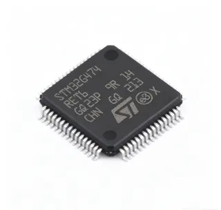
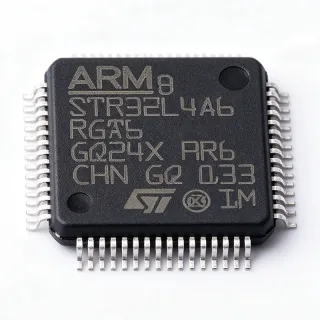
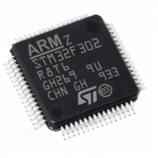
STM32G473RCT6 - 170MHz ARM Cortex-M4F MCU | STMicroelectronics
MPN: STM32G473RCT6 ✓ Active| Qty | Unit Price | Extended |
|---|---|---|
| 1 | $8.5 | $8.50 |
| 10 | $7.65 | $76.50 |
| 100 | $6.8 | $680.00 |
| 500 | $6.12 | $3,060.00 |
| 1,000 | $5.44 | $5,440.00 |
STM32G473RCT6 Overview
What is a microcontroller? A microcontroller (MCU) is a compact integrated circuit designed to govern a specific operation in an embedded system. It contains a processor core, memory (RAM and flash), and programmable input/output peripherals on a single chip. In the system hierarchy, a microcontroller is a type of embedded processor, which falls under the broader category of integrated circuits. The STM32G473RCT6 is a mid-range MCU in the STM32G4 family, positioned between the value-line STM32G0 and the high-performance STM32H7 series, offering a balance of performance, analog integration, and power efficiency.
Key features of the STM32G473RCT6 include a 256 KB flash memory and 128 KB SRAM, a 170 MHz CPU with DSP instructions and FPU, and a comprehensive set of peripherals: 4x 12-bit DACs, 5x 12-bit ADCs with hardware oversampling, 6x ultra-fast comparators, 4x operational amplifiers, and 2x advanced motor-control timers. It also supports a wide range of communication interfaces including SPI, I2C, USART, CAN FD, and USB. The device operates from 1.71V to 3.6V and is available in a 64-pin LQFP package.
The STM32G473RCT6 leverages ST's advanced 90nm process technology, enabling high performance with low power consumption. The Cortex-M4 core with FPU accelerates mathematical computations, making it ideal for real-time control loops in motor control and digital power conversion. The device also includes a memory protection unit (MPU), a cyclic redundancy check (CRC) unit, and a true random number generator (TRNG) for enhanced security and reliability.
Typical applications include field-oriented control (FOC) of brushless DC (BLDC) motors, digital power supplies (buck, boost, and flyback converters), solar inverters, and industrial automation. The rich analog peripherals allow for single-chip solutions that reduce BOM cost and board space. For example, in a motor control application, the integrated op-amps and comparators can directly interface with current-sensing resistors, eliminating the need for external signal conditioning.
When designing with this device, pay attention to the power supply decoupling: place a 100nF capacitor close to each VDD pin and a 4.7uF capacitor at the main power input. The VDDA pin must be connected to a clean analog supply, and the VREF+ pin should be decoupled with a 1uF capacitor to ensure ADC accuracy. Also, configure the clock system properly using the internal HSI16 oscillator or an external crystal for precise timing.
Drop-in alternatives for STM32G473RCT6 — same package, pin-to-pin compatible. Different-package parts requiring PCB rework are excluded.
Variants in this series
Same-series models that are drop-in compatible with STM32G473RCT6 (same form factor and footprint) — differing in Communication Interfaces, Core, Flash Memory, SRAM, ADC Resolution.
Quick Comparison Tool — Select alternative parts for side-by-side comparison:
STM32G474RCT6
✅ Drop-In ⚠️ Specs Unverified📋 Reference alternative (not in catalog)
STM32G473RBT6
✅ Drop-In ⚠️ Specs Unverified📋 Reference alternative (not in catalog)
STM32G474RBT6
✅ Drop-In ⚠️ Specs Unverified📋 Reference alternative (not in catalog)
STM32G431RBT6
✅ Drop-In ⚠️ Specs Unverified📋 Reference alternative (not in catalog)
STM32G431RCT6
✅ Drop-In ⚠️ Specs Unverified📋 Reference alternative (not in catalog)
STM32G441RBT6
✅ Drop-In ⚠️ Specs Unverified📋 Reference alternative (not in catalog)
STM32G441RCT6
✅ Drop-In ⚠️ Specs Unverified📋 Reference alternative (not in catalog)
STM32G491RCT6
✅ Drop-In ⚠️ Specs Unverified📋 Reference alternative (not in catalog)
STM32G491RET6
✅ Drop-In ⚠️ Specs Unverified📋 Reference alternative (not in catalog)
STM32G4A1RET6
✅ Drop-In ⚠️ Specs Unverified✓ In Stock
$5.44 / Unit
View Datasheet →STM32G4A1RCT6
✅ Drop-In ⚠️ Specs Unverified📋 Reference alternative (not in catalog)
STM32G4A1RGT6
✅ Drop-In ⚠️ Specs Unverified📋 Reference alternative (not in catalog)
STM32G4A1RGT6
✅ Drop-In ⚠️ Specs Unverified📋 Reference alternative (not in catalog)
STM32G4A1RGT6
✅ Drop-In ⚠️ Specs Unverified📋 Reference alternative (not in catalog)
STM32G4A1RGT6
✅ Drop-In ⚠️ Specs Unverified📋 Reference alternative (not in catalog)
STM32G4A1RGT6
✅ Drop-In ⚠️ Specs Unverified📋 Reference alternative (not in catalog)
STM32G4A1RGT6
✅ Drop-In ⚠️ Specs Unverified📋 Reference alternative (not in catalog)
STM32G4A1RGT6
✅ Drop-In ⚠️ Specs Unverified📋 Reference alternative (not in catalog)
STM32G4A1RGT6
✅ Drop-In ⚠️ Specs Unverified📋 Reference alternative (not in catalog)
STM32G4A1RGT6
✅ Drop-In ⚠️ Specs Unverified📋 Reference alternative (not in catalog)
STM32G473RCT6 Maximum Ratings & Electrical Characteristics
| Core | ARM Cortex-M4 with FPU |
| Maximum Clock Frequency | 170 MHz |
| Flash Memory | 256 KB |
| SRAM | 128 KB |
| Supply Voltage Range | 1.71 V to 3.6 V |
| Package | LQFP-64 (10x10 mm) |
| Operating Temperature Range | -40C to +85C |
| Number of GPIOs | 51 |
| ADC Resolution | 12-bit |
| Number of ADCs | 5 |
| DAC Resolution | 12-bit |
| Number of DACs | 4 |
| Number of Timers | 12 (including 2 advanced motor-control timers) |
| Communication Interfaces | SPI, I2C, USART, CAN FD, USB |
| DMA Channels | 16 |
| RoHS Status | Compliant |
STM32G473RCT6 Pin Configuration
| Pin 1 | VBAT — Battery backup supply |
| Pin 2 | PC13 — GPIO / RTC output |
| Pin 3 | PC14 — GPIO / OSC32_IN |
| Pin 4 | PC15 — GPIO / OSC32_OUT |
| Pin 5 | PF0 — GPIO |
| Pin 6 | PF1 — GPIO |
| Pin 7 | NRST — Reset (active low) |
| Pin 8 | VDD — Digital power supply |
| Pin 9 | VSS — Ground |
| Pin 10 | VDDA — Analog power supply |
| Pin 11 | PA0 — GPIO / ADC input |
| Pin 12 | PA1 — GPIO / ADC input |
| Pin 13 | PA2 — GPIO / USART2_TX |
| Pin 14 | PA3 — GPIO / USART2_RX |
| Pin 15 | PA4 — GPIO / DAC_OUT1 |
| Pin 16 | PA5 — GPIO / DAC_OUT2 |
| Pin 17 | PA6 — GPIO / TIM1_CH1 |
| Pin 18 | PA7 — GPIO / TIM1_CH2 |
| Pin 19 | PA8 — GPIO / TIM1_CH1 |
| Pin 20 | PA9 — GPIO / USART1_TX |
| Pin 21 | PA10 — GPIO / USART1_RX |
| Pin 22 | PA11 — GPIO / USB_DM |
| Pin 23 | PA12 — GPIO / USB_DP |
| Pin 24 | PA13 — GPIO / SWDIO |
| Pin 25 | PA14 — GPIO / SWCLK |
| Pin 26 | PA15 — GPIO / JTDI |
| Pin 27 | PB0 — GPIO / ADC input |
| Pin 28 | PB1 — GPIO / ADC input |
| Pin 29 | PB2 — GPIO / BOOT1 |
| Pin 30 | PB3 — GPIO / JTDO |
| Pin 31 | PB4 — GPIO / NJTRST |
| Pin 32 | PB5 — GPIO / I2C1_SMBA |
| Pin 33 | PB6 — GPIO / I2C1_SCL |
| Pin 34 | PB7 — GPIO / I2C1_SDA |
| Pin 35 | PB8 — GPIO / CAN1_RX |
| Pin 36 | PB9 — GPIO / CAN1_TX |
| Pin 37 | PB10 — GPIO / I2C2_SCL |
| Pin 38 | PB11 — GPIO / I2C2_SDA |
| Pin 39 | PB12 — GPIO / SPI2_NSS |
| Pin 40 | PB13 — GPIO / SPI2_SCK |
| Pin 41 | PB14 — GPIO / SPI2_MISO |
| Pin 42 | PB15 — GPIO / SPI2_MOSI |
| Pin 43 | PC0 — GPIO / ADC input |
| Pin 44 | PC1 — GPIO / ADC input |
| Pin 45 | PC2 — GPIO / ADC input |
| Pin 46 | PC3 — GPIO / ADC input |
| Pin 47 | PC4 — GPIO / ADC input |
| Pin 48 | PC5 — GPIO / ADC input |
| Pin 49 | PC6 — GPIO / TIM3_CH1 |
| Pin 50 | PC7 — GPIO / TIM3_CH2 |
| Pin 51 | PC8 — GPIO / TIM3_CH3 |
| Pin 52 | PC9 — GPIO / TIM3_CH4 |
| Pin 53 | PC10 — GPIO / USART4_TX |
| Pin 54 | PC11 — GPIO / USART4_RX |
| Pin 55 | PC12 — GPIO / USART5_TX |
| Pin 56 | PD0 — GPIO / CAN2_RX |
| Pin 57 | PD1 — GPIO / CAN2_TX |
| Pin 58 | PD2 — GPIO / TIM1_ETR |
| Pin 59 | VDD — Digital power supply |
| Pin 60 | VSS — Ground |
| Pin 61 | PD3 — GPIO / USART2_CTS |
| Pin 62 | PD4 — GPIO / USART2_RTS |
| Pin 63 | PD5 — GPIO / USART2_TX |
| Pin 64 | PD6 — GPIO / USART2_RX |
Typical Applications
STM32G473RCT6 is suitable for 6 applications: Motor Control, Digital Power Conversion, Industrial Automation, Solar Inverters, Battery Management Systems, Test and Measurement.
Motor Control
The STM32G473RCT6 is ideal for field-oriented control (FOC) of brushless DC (BLDC) motors and permanent magnet synchronous motors (PMSM). Its 170 MHz Cortex-M4F core with FPU accelerates complex control algorithms, while the integrated operational amplifiers and comparators enable direct current sensing and overcurrent protection without external components. The advanced motor-control timers (TIM1 and TIM8) generate complementary PWM signals with programmable dead-time, ensuring efficient and safe motor driving. In a typical FOC application, the MCU reads phase currents via the internal op-amps, processes the Clarke and Park transforms in real-time, and outputs PWM signals to the inverter. The high-resolution ADCs (up to 12-bit with hardware oversampling) provide accurate current feedback, and the fast comparators can trigger emergency shutdown in under 100 ns. This integration reduces BOM cost and board space, making it suitable for compact motor drives in appliances, drones, and industrial robots.
Recommended
Digital Power Conversion
The STM32G473RCT6 excels in digital power supplies, including buck, boost, and flyback converters. Its high-speed ADCs (up to 4 Msps) and comparators enable precise voltage and current monitoring, while the advanced timers generate PWM signals with high resolution (up to 184 ps). The integrated DACs can be used for reference voltage generation or as part of a digital-to-analog control loop. In a typical digital buck converter, the MCU reads the output voltage via an ADC, runs a PID control algorithm, and adjusts the PWM duty cycle to maintain regulation. The fast comparators can detect overcurrent conditions and trigger a fault shutdown within microseconds. The device's 170 MHz clock ensures the control loop can run at high bandwidth, improving transient response. Additionally, the CAN FD interface allows communication with a host controller for telemetry and configuration. This makes the STM32G473RCT6 a cost-effective solution for server power supplies, telecom rectifiers, and battery chargers.
Recommended
Industrial Automation
In industrial automation, the STM32G473RCT6 serves as a central controller for PLCs, sensors, and actuators. Its rich set of communication interfaces (CAN FD, USB, SPI, I2C, USART) allows seamless integration with industrial networks such as CANopen and Modbus. The device's robust design, with operating temperature up to 85C and ESD protection, ensures reliability in harsh environments. The multiple timers and DMA channels enable efficient handling of multiple tasks, such as reading encoder inputs, controlling stepper motors, and managing communication protocols. The integrated analog peripherals can interface with temperature sensors, pressure sensors, and current transducers without external ADCs. In a typical PLC I/O module, the MCU reads digital inputs, processes logic, and drives outputs via the GPIOs or timers. The low power consumption (down to 100 uA in standby mode) is beneficial for battery-powered field devices. The device's security features, including a true random number generator and memory protection unit, enhance system integrity.
Recommended
Solar Inverters
The STM32G473RCT6 is well-suited for solar microinverters and string inverters. Its high-performance core and advanced analog peripherals enable maximum power point tracking (MPPT) algorithms and grid-tie control. The multiple ADCs can simultaneously sample PV voltage, current, and grid voltage, while the comparators provide fast overcurrent protection. The advanced timers generate PWM signals for the DC-DC boost converter and the DC-AC inverter stage. The device's 170 MHz clock ensures the control loop can track the MPPT point quickly, maximizing energy harvest. The CAN FD interface allows communication with a central monitoring system. In a typical microinverter, the MCU runs a perturb-and-observe MPPT algorithm, adjusts the boost converter duty cycle, and controls the H-bridge inverter to synchronize with the grid. The integrated op-amps can condition the current sense signals, reducing external component count. The device's wide operating temperature range and robust design make it suitable for outdoor installation.
Recommended
Battery Management Systems
The STM32G473RCT6 can be used in battery management systems (BMS) for electric vehicles, energy storage, and portable devices. Its multiple ADCs can monitor cell voltages and temperatures, while the CAN FD interface enables communication with the vehicle's main controller. The device's low power modes help extend battery life in standby. The integrated comparators can detect overvoltage and undervoltage conditions, triggering protection actions. In a typical BMS, the MCU reads each cell voltage via a multiplexed ADC, calculates the state of charge (SoC) using algorithms, and controls balancing circuits. The high-resolution ADCs (12-bit) provide accurate voltage measurements, and the DMA channels allow continuous monitoring without CPU intervention. The device's security features, including a unique ID and CRC unit, enhance system integrity. The wide operating temperature range (-40C to 85C) is suitable for automotive and industrial environments.
Recommended
Test and Measurement
The STM32G473RCT6 is used in test and measurement equipment such as data loggers, oscilloscopes, and signal generators. Its high-speed ADCs (up to 4 Msps) and DACs enable precise signal acquisition and generation. The multiple timers can generate precise time bases for triggering and sampling. The USB interface allows easy connection to a PC for data transfer and control. In a typical data logger, the MCU samples analog signals at high rates, stores data in SRAM or external memory, and streams it to a host via USB. The device's DMA channels enable continuous sampling without CPU overhead. The integrated op-amps can buffer input signals, and the comparators can detect threshold crossings for triggering. The device's low power consumption is beneficial for portable instruments. The rich set of peripherals allows a single-chip solution for many test and measurement applications, reducing cost and complexity.
Recommended
Recommended Products Summary
Engineering reference data for STM32G473RCT6 — comparison, design guidance, and compliance information.
Selection Guide
Comparison with Alternatives
| Parameter | This Product | STM32G474RCT6 | STM32G473RBT6 | STM32G431RBT6 |
|---|---|---|---|---|
| Package | LQFP-64 | LQFP-64 | LQFP-64 | LQFP-64 |
| Brand | STMicroelectronics | STMicroelectronics | STMicroelectronics | STMicroelectronics |
| Core | ARM Cortex-M4F | ARM Cortex-M4F | ARM Cortex-M4F | ARM Cortex-M4F |
| Maximum Clock Frequency | 170 MHz | 170 MHz | 170 MHz | 170 MHz |
| Flash Memory | 256 KB | 256 KB | 128 KB | 128 KB |
| SRAM | 128 KB | 128 KB | 128 KB | 32 KB |
| Number of DACs | 4 | 5 | 4 | 2 |
| Number of Comparators | 6 | 7 | 6 | 4 |
| Number of Op-Amps | 4 | 4 | 4 | 3 |
| CAN FD | Yes | Yes | Yes | Yes |
Key Differentiators
- Higher analog integration (vs STM32G431RBT6)
- More memory (vs STM32G473RBT6)
- Cost-effective alternative to G474 (vs STM32G474RCT6)
Design Notes
Decouple each VDD pin with a 100nF ceramic capacitor placed as close as possible to the pin. Additionally, place a 4.7uF capacitor at the main power input. The VDDA pin must be connected to a clean analog supply, and VREF+ should be decoupled with a 1uF capacitor to ensure ADC accuracy. Use a ferrite bead between VDD and VDDA to filter high-frequency noise.
For the LQFP-64 package, ensure proper grounding: use a solid ground plane under the device. Route high-speed signals (e.g., SPI, USB) with controlled impedance and keep traces short. For motor control applications, separate power and signal grounds to avoid noise coupling. Place the crystal oscillator close to the OSC_IN/OSC_OUT pins and keep the load capacitors within 5mm.
Do not exceed the absolute maximum ratings: VDD must not exceed 3.6V, and any pin voltage must not exceed VDD+0.3V. Ensure the BOOT0 pin is configured correctly to avoid accidental boot from system memory. When using the ADC, set the sampling time appropriately for the source impedance to avoid inaccurate readings. Also, configure the clock system properly using the internal HSI16 or an external crystal to avoid timing issues.
Compliance Information
RoHS compliant per STMicroelectronics product page. Not AEC-Q100 qualified; for automotive, consider STM32G4A1 series.