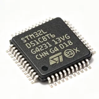
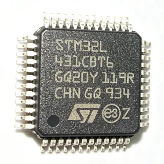
STM32L081CBT6 - Ultra-Low-Power ARM Cortex-M0+ MCU | STMicroelectronics
MPN: STM32L081CBT6 ✓ Active| Qty | Unit Price | Extended |
|---|---|---|
| 1 | $3.42 | $3.42 |
| 10 | $3.08 | $30.80 |
| 100 | $2.74 | $274.00 |
| 500 | $2.47 | $1,235.00 |
| 1,000 | $2.19 | $2,190.00 |
STM32L081CBT6 Overview
An ultra-low-power microcontroller (MCU) is a type of integrated circuit that combines a processor core, memory, and peripherals on a single chip, optimized for minimal power consumption. It is a key component in the hierarchy of embedded systems, where it serves as the central processing unit for devices that require long battery life, such as wearables, IoT sensors, and medical monitors. The STM32L0 series is part of the broader STM32 family, which includes higher-performance Cortex-M3/M4/M7 variants, but the L0 series specifically targets power-sensitive applications.
Key features of the STM32L081CBT6 include multiple low-power modes (Sleep, Low-power Run, Low-power Sleep, Stop, Standby), a 12-bit ADC with hardware oversampling, a 12-bit DAC, two comparators, and a USB 2.0 full-speed device controller. It also integrates a real-time clock (RTC) with calendar and alarm functions, and a true EEPROM emulation using the Flash memory. The device supports a wide supply voltage range from 1.65V to 3.6V, making it suitable for single-cell battery operation.
The STM32L081CBT6 is built on ST's ultra-low-leakage process technology, achieving dynamic power consumption as low as 84 µA/MHz in Run mode and 0.29 µA in Standby mode with RTC. This is achieved through a flexible clock gating and power management architecture that allows each peripheral to be independently powered down. The device also includes a hardware cryptographic accelerator (AES-128) for secure data communication.
Typical applications include battery management systems, portable medical devices, smart sensors, and IoT nodes. The USB interface enables direct connectivity to hosts for data logging or firmware updates. The rich analog peripherals make it ideal for signal conditioning and measurement applications.
When designing with this MCU, careful attention should be paid to the power supply decoupling and the selection of the appropriate low-power mode to balance performance and energy consumption. The device's extensive documentation and STM32Cube ecosystem provide a robust development environment, including HAL libraries and low-layer APIs.
Drop-in alternatives for STM32L081CBT6 — same package, pin-to-pin compatible. Different-package parts requiring PCB rework are excluded.
Variants in this series
Same-series models that are drop-in compatible with STM32L081CBT6 (same form factor and footprint) — differing in Flash Memory, RTC.
Quick Comparison Tool — Select alternative parts for side-by-side comparison:
STM32L071CBT6
✅ Drop-In ⚠️ Specs Unverified✓ In Stock
$2.19 / Unit
View Datasheet →STM32L081CBT6TR
✅ Drop-In ⚠️ Specs Unverified📋 Reference alternative (not in catalog)
STM32L081CBT7
✅ Drop-In ⚠️ Specs Unverified📋 Reference alternative (not in catalog)
STM32L082CBT6
✅ Drop-In ⚠️ Specs Unverified📋 Reference alternative (not in catalog)
STM32L071CBT7
✅ Drop-In ⚠️ Specs Unverified✓ In Stock
$8.1244 / Unit
View Datasheet →STM32L081CBT6 Maximum Ratings & Electrical Characteristics
| Core | ARM Cortex-M0+ |
| Maximum Frequency | 32 MHz |
| Flash Memory | 192 KB |
| SRAM | 20 KB |
| Package | LQFP-48 (7x7 mm) |
| Supply Voltage Range | 1.65 V to 3.6 V |
| Operating Temperature Range | -40C to +85C |
| ADC | 12-bit, 16 channels, with hardware oversampling |
| DAC | 12-bit, 1 channel |
| Comparators | 2 |
| USB | USB 2.0 full-speed device |
| RTC | Calendar and alarm, with backup registers |
| AES | 128-bit hardware encryption |
| Low-power modes | Sleep, Low-power Run, Low-power Sleep, Stop, Standby |
| Dynamic power consumption | 84 µA/MHz in Run mode |
| Standby current | 0.29 µA with RTC |
| GPIO | Up to 37 I/Os |
| Communication interfaces | I2C, SPI, USART, LPUART |
| RoHS Status | Compliant |
STM32L081CBT6 Pin Configuration
| Pin 1 | VBAT — Backup battery supply for RTC and backup registers |
| Pin 2 | PC14/OSC32_IN — GPIO or 32.768 kHz oscillator input |
| Pin 3 | PC15/OSC32_OUT — GPIO or 32.768 kHz oscillator output |
| Pin 4 | OSC_IN — Main oscillator input |
| Pin 5 | OSC_OUT — Main oscillator output |
| Pin 6 | NRST — Reset (active low) |
| Pin 7 | VSSA — Analog ground |
| Pin 8 | VDDA — Analog power supply |
| Pin 9 | PA0 — GPIO/ADC input |
| Pin 10 | PA1 — GPIO/ADC input |
| Pin 11 | PA2 — GPIO/USART2_TX |
| Pin 12 | PA3 — GPIO/USART2_RX |
| Pin 13 | PA4 — GPIO/SPI1_NSS |
| Pin 14 | PA5 — GPIO/SPI1_SCK |
| Pin 15 | PA6 — GPIO/SPI1_MISO |
| Pin 16 | PA7 — GPIO/SPI1_MOSI |
| Pin 17 | PB0 — GPIO/ADC input |
| Pin 18 | PB1 — GPIO/ADC input |
| Pin 19 | PB2 — GPIO |
| Pin 20 | PB10 — GPIO/I2C2_SCL |
| Pin 21 | PB11 — GPIO/I2C2_SDA |
| Pin 22 | PB12 — GPIO/SPI2_NSS |
| Pin 23 | PB13 — GPIO/SPI2_SCK |
| Pin 24 | PB14 — GPIO/SPI2_MISO |
| Pin 25 | PB15 — GPIO/SPI2_MOSI |
| Pin 26 | PC13 — GPIO/RTC_TAMP1 |
| Pin 27 | PC14 — GPIO/OSC32_IN |
| Pin 28 | PC15 — GPIO/OSC32_OUT |
| Pin 29 | VSS — Ground |
| Pin 30 | VDD — Power supply |
| Pin 31 | PA8 — GPIO/USB_DP |
| Pin 32 | PA9 — GPIO/USB_DM |
| Pin 33 | PA10 — GPIO/USART1_RX |
| Pin 34 | PA11 — GPIO/USART1_TX |
| Pin 35 | PA12 — GPIO/SPI1_NSS |
| Pin 36 | PA13 — GPIO/SWDIO |
| Pin 37 | PA14 — GPIO/SWCLK |
| Pin 38 | PA15 — GPIO/SPI1_NSS |
| Pin 39 | PB3 — GPIO/SPI1_SCK |
| Pin 40 | PB4 — GPIO/SPI1_MISO |
| Pin 41 | PB5 — GPIO/SPI1_MOSI |
| Pin 42 | PB6 — GPIO/I2C1_SCL |
| Pin 43 | PB7 — GPIO/I2C1_SDA |
| Pin 44 | PB8 — GPIO/I2C1_SCL |
| Pin 45 | PB9 — GPIO/I2C1_SDA |
| Pin 46 | VDD — Power supply |
| Pin 47 | VSS — Ground |
| Pin 48 | VDD — Power supply |
Typical Applications
STM32L081CBT6 is suitable for 6 applications: Battery Management Systems, IoT Sensor Nodes, Portable Medical Devices, Smart Sensors, Wearable Devices, Industrial Control.
Battery Management Systems
The STM32L081CBT6 is ideal for battery management systems (BMS) in portable electronics and electric vehicles. Its ultra-low-power modes extend battery life, while the 12-bit ADC with oversampling enables accurate voltage and current monitoring. The device can manage cell balancing, state-of-charge estimation, and protection algorithms. Its wide supply voltage range (1.65V-3.6V) allows direct connection to battery cells, and the AES-128 encryption secures communication with the host. The RTC with calendar and alarm functions supports time-stamping of events. In a typical BMS, the MCU reads cell voltages via the ADC, controls balancing FETs via GPIO, and communicates with a host over I2C or USART. The low-power Stop mode can be used during idle periods to minimize drain, while the device wakes periodically to perform measurements. The STM32L081CBT6's robust analog front-end and low power consumption make it a cost-effective choice for BMS designs.
Recommended
IoT Sensor Nodes
The STM32L081CBT6 is well-suited for IoT sensor nodes that require long battery life and reliable wireless connectivity. Its ultra-low-power consumption (84 µA/MHz) and multiple low-power modes allow the device to sleep for extended periods, waking only to take sensor readings and transmit data. The integrated AES-128 encryption ensures secure communication with cloud services. The device supports various communication interfaces (I2C, SPI, USART, LPUART) to interface with sensors such as temperature, humidity, and motion detectors. In a typical IoT node, the MCU wakes from Stop mode, reads sensor data via I2C, processes it, and sends it to a wireless module (e.g., LoRa, BLE) via UART. The LPUART interface is specifically designed for low-power communication, further reducing energy consumption. The STM32L081CBT6's small LQFP-48 package and wide supply voltage range make it easy to integrate into compact, battery-powered designs.
Recommended
Portable Medical Devices
The STM32L081CBT6 is an excellent choice for portable medical devices such as glucose meters, pulse oximeters, and wearable health monitors. Its ultra-low-power operation ensures long battery life, critical for devices that must operate for months on a single coin cell. The 12-bit ADC with hardware oversampling provides high-resolution measurements for biosignals, while the 12-bit DAC can generate analog waveforms for stimulation or calibration. The device's small footprint and low component count make it ideal for compact, wearable designs. In a pulse oximeter, the MCU controls an LED driver, reads photodiode signals via the ADC, and calculates SpO2 levels. The USB interface allows for data transfer to a PC or smartphone for analysis. The STM32L081CBT6's reliability and low power consumption make it a trusted choice for medical applications.
Recommended
Smart Sensors
The STM32L081CBT6 is perfect for smart sensors in industrial and building automation. Its rich analog peripherals (ADC, DAC, comparators) allow direct interfacing with various sensor types, while its low-power modes enable battery or energy-harvesting operation. The device can perform local signal processing, reducing the data sent to a central controller. For example, in a smart thermostat, the MCU reads temperature and humidity sensors, implements a control algorithm, and drives an actuator via PWM. The AES-128 encryption secures communication with the building management system. The STM32L081CBT6's wide operating temperature range (-40C to +85C) makes it suitable for harsh environments. Its multiple communication interfaces (I2C, SPI, USART) allow easy integration with existing industrial networks.
Recommended
Wearable Devices
The STM32L081CBT6 is an ideal microcontroller for wearable devices like fitness trackers and smartwatches. Its ultra-low-power consumption is essential for devices that run on small batteries and are worn continuously. The device's small LQFP-48 package and low pin count make it suitable for compact PCB designs. The integrated USB controller allows for easy charging and data synchronization. The 12-bit ADC can interface with various biometric sensors, such as heart-rate monitors and accelerometers. In a fitness tracker, the MCU collects accelerometer data, processes steps, and displays information on an OLED display via SPI. The device can enter Standby mode when not in use, waking periodically to update the display or log data. The STM32L081CBT6's combination of low power, rich peripherals, and small size makes it a top choice for wearables.
Recommended
Industrial Control
The STM32L081CBT6 is suitable for industrial control applications such as motor control, process monitoring, and automation. Its robust design, wide operating temperature range, and rich peripheral set make it a reliable choice for harsh environments. The device's multiple timers and PWM outputs can control motors and actuators, while the ADC and comparators monitor analog signals. The AES-128 encryption ensures secure communication in industrial networks. In a motor control application, the MCU generates PWM signals to drive a motor driver, reads encoder feedback via a timer, and implements a PID control loop. The low-power modes can be used to reduce energy consumption during idle periods. The STM32L081CBT6's industrial-grade reliability and long-term availability make it a preferred choice for industrial designs.
Recommended
Recommended Products Summary
Engineering reference data for STM32L081CBT6 — comparison, design guidance, and compliance information.
Selection Guide
Comparison with Alternatives
| Parameter | This Product | STM32L071CBT6 | STM32L081CBT6TR | STM32L081CBT7 | STM32L082CBT6 |
|---|---|---|---|---|---|
| Package | LQFP-48 | LQFP-48 | LQFP-48 | LQFP-48 | LQFP-48 |
| Brand | STMicroelectronics | STMicroelectronics | STMicroelectronics | STMicroelectronics | STMicroelectronics |
| Core | ARM Cortex-M0+ | ARM Cortex-M0+ | ARM Cortex-M0+ | ARM Cortex-M0+ | ARM Cortex-M0+ |
| Maximum Frequency | 32 MHz | 32 MHz | 32 MHz | 32 MHz | 32 MHz |
| Flash Memory | 192 KB | 192 KB | 192 KB | 192 KB | 192 KB |
| SRAM | 20 KB | 20 KB | 20 KB | 20 KB | 20 KB |
| USB | Yes (full-speed) | No | Yes (full-speed) | Yes (full-speed) | Yes (full-speed) |
| DAC | Yes (12-bit) | No | Yes (12-bit) | Yes (12-bit) | Yes (12-bit) |
| Operating Temperature Range | -40C to +85C | -40C to +85C | -40C to +85C | -40C to +105C | -40C to +85C |
Key Differentiators
- Integrated USB 2.0 full-speed device controller (vs STM32L071CBT6)
- 12-bit DAC with output buffer (vs STM32L071CBT6)
- Hardware AES-128 encryption (vs STM32L071CBT6)
Design Notes
Decouple the VDD and VDDA pins with 100 nF ceramic capacitors placed as close to the pins as possible. Additionally, use a 1 µF capacitor on VDDA for analog noise filtering. For battery-powered designs, consider using the low-power modes (Stop, Standby) to minimize current consumption. The VBAT pin should be connected to a backup battery or tied to VDD if not used.
For the LQFP-48 package, ensure proper soldering by following the recommended land pattern in the datasheet. Provide a solid ground plane to reduce noise and improve thermal performance. Keep high-speed signals (e.g., SPI, USB) away from the oscillator pins to avoid interference. Use a 32.768 kHz crystal for the RTC with load capacitors as specified in the datasheet.
Do not exceed the absolute maximum ratings for VDD (3.6V) and VDDA (3.6V). Ensure that the NRST pin is properly pulled up with a 100 nF capacitor to ground for reliable reset. When using the USB interface, ensure that the USB_DP and USB_DM pins are correctly routed with 22 Ω series resistors and proper impedance matching. Also, configure the GPIO pins correctly to avoid floating inputs, which can increase power consumption.
Compliance Information
RoHS compliant per STMicroelectronics product page. Not AEC-Q100 qualified - this is a general-purpose MCU, not automotive grade.