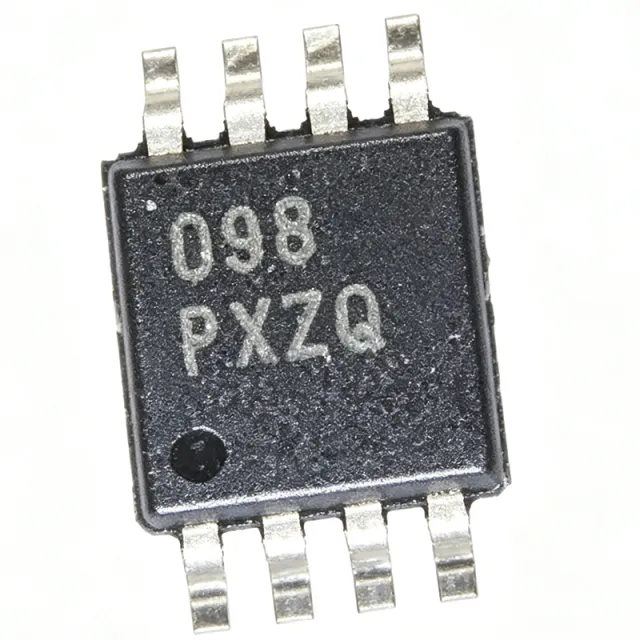
TPS7A1601QDGNRQ1 - 60V 100mA LDO 5uA IQ AEC-Q100 | Texas Instruments
MPN: TPS7A1601QDGNRQ1 ✓ Active| Qty | Unit Price | Extended |
|---|---|---|
| 1 | $2.54 | $2.54 |
| 10 | $2.29 | $22.90 |
| 100 | $2.03 | $203.00 |
| 500 | $1.87 | $935.00 |
| 1,000 | $1.66 | $1,660.00 |
TPS7A1601QDGNRQ1 Overview
An LDO (low-dropout regulator) is a type of linear voltage regulator that maintains a stable output voltage even when the input-output differential is small. Within the power management IC hierarchy, LDOs provide ripple-free regulation downstream of switching converters or directly from harsh input rails. The TPS7A16-Q1 family targets wide-VIN battery and automotive systems where high input tolerance and ultra-low standby current are critical.
Key features include a 4.5V to 60V input range with integrated undervoltage lockout (UVLO), 5uA quiescent current for always-on battery applications, CMOS-logic-compatible enable pin, and an integrated open-drain, active-high power-good (PG) output with user-programmable delay for rail sequencing. The device is AEC-Q100 qualified for -40C to +125C operation.
Architecturally, the TPS7A16-Q1 uses a precision reference and error amplifier with internal protection including current limiting and thermal shutdown. The PowerPAD HVSSOP-8 package provides low thermal resistance, allowing reliable 100mA operation from high input voltages when the exposed pad is soldered to an adequate copper plane. Adjustable output is set with two external resistors using the standard feedback divider equation.
Typical applications include automotive battery-connected rails (12V/24V/48V systems), always-on microcontroller standby supplies, battery-powered industrial sensors, and power-rail sequencing in MCU-based systems where the PG output enables controlled startup. The 60V rating provides surge margin on automotive load-dump-exposed nodes.
Design consideration: at 60V input and low output voltage, power dissipation limits output current; calculate Pd = (VIN - VOUT) x IOUT and ensure the thermal design keeps junction temperature below 125C.
This page synthesizes distributor pricing, drop-in alternatives, and practical design notes not found in the manufacturer datasheet. Prices shown are as of 2026-09-01.
Drop-in alternatives for TPS7A1601QDGNRQ1 — same package, pin-to-pin compatible. Different-package parts requiring PCB rework are excluded.
Variants in this series
Same-series models that are drop-in compatible with TPS7A1601QDGNRQ1 (same form factor and footprint) — differing in Input Voltage Range, Package, Power Good Output, Protection Features.
Quick Comparison Tool — Select alternative parts for side-by-side comparison:
TPS7A1601DGNR
✅ Drop-In✓ In Stock
$0.98 / Unit
View Datasheet →TPS7A1650QDGNRQ1
✅ Drop-In📋 Reference alternative (not in catalog)
TPS7A1633QDGNRQ1
✅ Drop-In📋 Reference alternative (not in catalog)
TPS7A3001DGNR
✅ Drop-In📋 Reference alternative (not in catalog)
TPS7A1601QDGNRQ1 Maximum Ratings & Electrical Characteristics
| Output Type | Adjustable |
| Output Voltage Range | 1.2 V to 18.5 V |
| Maximum Output Current | 100 mA |
| Input Voltage Range | 4.5 V to 60 V |
| Quiescent Current (IQ) | 5 uA |
| Number of Regulators | 1 |
| Polarity | Positive |
| Enable Pin | Yes (CMOS-logic compatible) |
| Power Good Output | Yes (open-drain, active-high, user-programmable delay) |
| Undervoltage Lockout | Yes (UVLO integrated) |
| Protection Features | Current limiting, thermal shutdown |
| Operating Temperature | -40C to +125C |
| Qualification | AEC-Q100 (automotive) |
| Package | HVSSOP-8 (MSOP-PowerPAD, DGN), 8 pins |
| Mounting Type | Surface Mount |
| Marking Code | PXZQ |
TPS7A1601QDGNRQ1 Pin Configuration
| Pin 1 | EN — Enable input, CMOS-logic compatible (active high) |
| Pin 2 | IN — Input supply (4.5V to 60V) |
| Pin 3 | IN — Input supply (internally connected to pin 2) |
| Pin 4 | GND — Ground |
| Pin 5 | PG — Power-good output, open-drain, active-high, with programmable delay |
| Pin 6 | OUT — Regulated output voltage |
| Pin 7 | FB — Feedback / adjust pin for adjustable output (TPS7A1601 variant) |
| Pin 8 | NC — Not connected (per datasheet) |
| Pin PAD | PowerPAD — Exposed thermal pad, solder to GND copper plane |
Typical Applications
TPS7A1601QDGNRQ1 is suitable for 6 applications: Automotive Battery-Connected Standby Rails, Always-On Microcontroller Standby Supply, 48V Automotive and Industrial Rail Housekeeping, Battery-Powered Industrial Sensors, Multi-Rail Power Sequencing in MCU Systems, Precision Analog and Reference Supplies.
Automotive Battery-Connected Standby Rails
The TPS7A1601QDGNRQ1 fits automotive always-on standby supplies because it connects directly to 12V, 24V, or 48V battery nodes with a 4.5V to 60V input range, absorbing load-dump-class transients without external surge suppression in many designs. Its 5uA quiescent current is the decisive parameter: a key-off module drawing even 1mA would drain a battery over weeks, whereas 5uA preserves state-of-charge for months. Placed between the battery node and an MCU standby rail with a small ceramic input capacitor and UVLO handling cold-crank conditions, the regulator maintains a clean low-noise output that switching converters cannot provide at such low standby power. Thermal dissipation must be checked at high VIN, but standby currents are typically a few milliamps, keeping losses in the tens of milliwatts.
Recommended
Always-On Microcontroller Standby Supply
Microcontroller-based systems that must wake instantly from sleep need a standby rail that stays powered continuously, and the TPS7A1601QDGNRQ1 serves this role with 5uA IQ and a 100mA capability for wake-up events. The CMOS-compatible enable pin lets the MCU or a system controller gate the rail when full shutdown is desired, dropping consumption to near zero, while the power-good output signals the MCU when the rail is stable after wake. The adjustable 1.2V to 18.5V output covers common 1.8V, 3.3V, and 5V standby rails from a single design. Compared with a buck converter, the LDO adds no switching noise that could corrupt sleep-mode analog peripherals, at the cost of higher dissipation during active high-current phases - acceptable when standby duty dominates the power budget.
Recommended
48V Automotive and Industrial Rail Housekeeping
The 60V input rating of the TPS7A1601QDGNRQ1 makes it directly suitable for housekeeping and bias rails on 48V battery systems found in mild-hybrid vehicles, telecom infrastructure, and industrial drives. Nominal 48V plus transient margin fits comfortably below the 60V absolute limit, and the integrated UVLO prevents erratic operation during brownout. The adjustable output up to 18.5V can generate gate-driver bias rails or analog supplies for supervisory circuits. Because the (VIN - VOUT) x IOUT dissipation grows quickly at 48V input, the PowerPAD exposed pad must be soldered to a substantial copper plane; at 50mA and a 43V differential, dissipation is roughly 2.15W, which a well-designed HVSSOP-8 thermal layout can manage within the -40C to +125C AEC-Q100 envelope.
Recommended
Battery-Powered Industrial Sensors
Industrial sensors running for years on a primary lithium cell or energy-harvesting supply benefit from the TPS7A1601QDGNRQ1 combination of 5uA quiescent current and 100mA peak capability for radio or ADC bursts. The 4.5V minimum input suits 2-series-cell or regulated battery buses, while the adjustable output supports low-voltage sensor cores. The power-good output provides a deterministic rail-valid flag so the MCU never samples sensors before the supply settles, improving measurement repeatability. Unlike a switching regulator, the linear topology produces no ripple or EMI that could degrade precision analog front ends in weigh-scale, pressure, or gas-sensing signal chains. The trade-off is efficiency at large VIN-VOUT differentials, so the sensor duty cycle should keep average current in the microamp-to-low-milliamp range.
Recommended
Multi-Rail Power Sequencing in MCU Systems
The TPS7A1601QDGNRQ1 open-drain, active-high power-good output with user-programmable delay is designed specifically for power-rail sequencing in microcontroller-based systems. Each regulator monitors its own output and asserts PG only after the rail reaches regulation and the programmed delay expires; cascading PG into the enable pin of the next regulator creates a deterministic startup order for core, I/O, and analog rails. This eliminates external supervisor ICs and RC-based delay circuits, saving board area in automotive clusters and industrial control modules. The AEC-Q100 qualification extends the scheme into environments with -40C cold-start requirements. Because PG is open-drain, it interfaces cleanly with rails of different voltage levels through a single pull-up resistor.
Recommended
Precision Analog and Reference Supplies
Low-noise analog circuits downstream of harsh automotive or industrial rails need a post-regulator that strips switching ripple without adding noise of its own, a role the TPS7A1601QDGNRQ1 fills as a wide-VIN LDO following a preregulating buck. The linear topology contributes no switching artifacts, and the 5uA IQ suits bias rails that must remain live in low-power modes. The adjustable output from 1.2V to 18.5V can feed voltage references, sensor excitation, or op-amp rails. Because PSRR and dropout degrade near the dropout region, maintain adequate VIN-VOUT headroom - typically at least 1V to 2V above the output at load - so the error amplifier retains loop gain. Verify junction temperature with the PowerPAD thermal model when the differential is large.
Recommended
Recommended Products Summary
Engineering reference data for TPS7A1601QDGNRQ1 — comparison, design guidance, and compliance information.
Selection Guide
Comparison with Alternatives
| Parameter | This Product | TPS7A1601DGNR | TPS7A1650QDGNRQ1 | TPS7A1633QDGNRQ1 | TPS7A3001DGNR |
|---|---|---|---|---|---|
| Package | HVSSOP-8 (DGN, PowerPAD) | HVSSOP-8 (DGN) - same | HVSSOP-8 (DGN) - same | HVSSOP-8 (DGN) - same | HVSSOP-8 (DGN) - same |
| Brand | Texas Instruments | Texas Instruments | Texas Instruments | Texas Instruments | Texas Instruments |
| Input Voltage Range | 4.5 V to 60 V | 4.5 V to 60 V | 4.5 V to 60 V | 4.5 V to 60 V | -3 V to -36 V (negative rail) |
| Output Voltage | Adjustable 1.2 V to 18.5 V | Adjustable 1.2 V to 18.5 V | Fixed 5.0 V | Fixed 3.3 V | Adjustable, negative |
| Output Current | 100 mA | 100 mA | 100 mA | 100 mA | 200 mA |
| Automotive Grade (AEC-Q100) | Yes (Q1) | No | Yes (Q1) | Yes (Q1) | No |
Key Differentiators
- Automotive AEC-Q100 qualification with PG and EN (vs TPS7A1601DGNR)
- Adjustable output up to 18.5V covers multiple rail voltages (vs TPS7A1650QDGNRQ1)
- Positive 60V wide-VIN rating (vs TPS7A3001DGNR)
- Fixed 3.3V variant for simplified BOM (vs TPS7A1633QDGNRQ1)
Design Notes
Estimated: power dissipation is Pd = (VIN - VOUT) x IOUT. At 60V in, 5V out, and 100mA, dissipation reaches 5.5W - far beyond what the HVSSOP-8 PowerPAD can dissipate without extreme measures, so full 100mA is only thermally feasible at small VIN-VOUT differentials. At 48V in and 50mA, dissipation is about 2.15W; solder the exposed PowerPAD to at least 1 square inch of 2oz copper and verify junction temperature stays below 125C using the theta_JA from the TI datasheet thermal table.
Solder the exposed PowerPAD to a solid ground plane with an array of thermal vias (typically 5x5 via grid under the pad) - this is not optional; the pad is the primary heat-removal path for the DGN package. Place the input ceramic capacitor within 5mm of the IN pins and the output capacitor close to OUT. Keep the FB divider resistor network close to the FB pin to minimize noise pickup on the adjustment node, and route the PG pull-up away from the FB trace to avoid coupling.
Do not exceed 60V on the IN pin - automotive load dump on 12V systems can exceed this without a transient suppressor such as a TVS diode. Do not float the EN pin in safety-critical designs; drive it actively or pull it up through a defined resistor. The PG output is open-drain and requires an external pull-up to a valid rail. When using the adjustable version, use 1%-tolerance feedback resistors and do not omit the recommended feedforward/output capacitors per the datasheet typical application, or stability and transient response will degrade.
Use the UVLO behavior deliberately in cold-crank and brownout scenarios: the regulator holds the output off until the input rises above the UVLO threshold, providing a clean startup. For sequencing designs, size the PG delay capacitor so downstream regulators enable only after the upstream rail has fully settled. In low-power designs, remember that feedback divider current adds to the 5uA IQ - use high-value (e.g., megaohm-range) divider resistors where the datasheet permits to preserve the ultra-low standby budget.
Compliance Information
AEC-Q100 qualified automotive grade per TI.com product page. RoHS/REACH status per TI standard product compliance; halogen-free status not explicitly stated in provided data.







