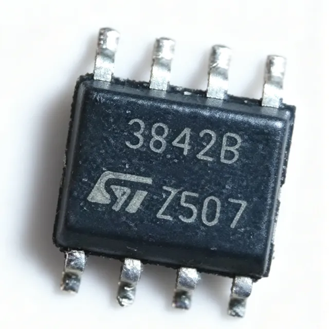
UC3842BD1 - Current Mode PWM Controller | STMicroelectronics | SMPS
MPN: UC3842BD1 ✓ Active| Qty | Unit Price | Extended |
|---|---|---|
| 1 | $0.2618 | $0.26 |
| 10 | $0.1891 | $1.89 |
| 100 | $0.1673 | $16.73 |
| 500 | $0.16 | $80.00 |
| 1,000 | $0.1527 | $152.70 |
| 2,500 | $0.1485 | $371.25 |
UC3842BD1 Overview
A current-mode PWM controller is a type of switching regulator control IC that regulates output voltage by comparing the output error signal with a current-sense signal from the power switch. This architecture provides inherent feed-forward compensation, cycle-by-cycle current limiting, and simplified loop compensation compared to voltage-mode controllers. The UC3842BD1 belongs to the UC3842 family of PWM controllers, which are widely used in AC-DC adapters, battery chargers, and industrial power supplies.
Key features of the UC3842BD1 include a trimmed oscillator for precise frequency control, an under-voltage lockout (UVLO) with hysteresis, a 5V reference output, and a high-gain error amplifier. The oscillator frequency is programmable up to 500 kHz, allowing designers to optimize transformer size and efficiency. The device also features a low startup current of 0.5 mA, which is critical for efficient power-up in battery-powered systems.
The UC3842BD1 uses a fixed-frequency current-mode architecture with a maximum duty cycle of 96%. The error amplifier has a bandwidth of 1 MHz, enabling fast transient response. The current-sense comparator has a threshold of 1V, providing accurate cycle-by-cycle current limiting. The device is designed to operate over a junction temperature range of -40°C to +150°C, ensuring reliability in harsh environments.
Typical applications include switch-mode power supplies (SMPS) for consumer electronics, industrial power converters, and battery chargers. The UC3842BD1 is also used in flyback and boost converter topologies, where its current-mode control simplifies loop compensation and improves line regulation.
When designing with the UC3842BD1, ensure that the current-sense resistor is placed close to the IC to minimize parasitic inductance. The oscillator timing resistor and capacitor should be located near the RT/CT pin to reduce noise coupling. Proper grounding and decoupling of the VCC pin are essential for stable operation.
This page synthesizes distributor pricing, drop-in alternatives, and practical design notes not found in the STMicroelectronics datasheet, providing engineers with a comprehensive resource for selecting and implementing the UC3842BD1.
Drop-in alternatives for UC3842BD1 — same package, pin-to-pin compatible. Different-package parts requiring PCB rework are excluded.
Variants in this series
Same-series models that are drop-in compatible with UC3842BD1 (same form factor and footprint) — differing in Package.
Quick Comparison Tool — Select alternative parts for side-by-side comparison:
UC3842BD
📋 Reference alternative (not in catalog)
UC3842BD1TR
📋 Reference alternative (not in catalog)
UC3842BD1G
📋 Reference alternative (not in catalog)
UC3842BD1 Maximum Ratings & Electrical Characteristics
| Input Voltage Range | 7.5 V to 30 V |
| Output Current (Peak) | 1 A |
| Oscillator Frequency (Max) | 500 kHz |
| Maximum Duty Cycle | 96% |
| Reference Output Voltage | 5 V |
| Reference Tolerance | ±2% |
| Error Amplifier Bandwidth | 1 MHz |
| Current Sense Threshold | 1 V |
| Startup Current | 0.5 mA |
| Operating Supply Current | 11 mA |
| Under-Voltage Lockout (UVLO) On | 16 V |
| Under-Voltage Lockout (UVLO) Off | 10 V |
| Operating Temperature Range | -40°C to +150°C |
| Package | SOIC-8 |
| Mounting Type | Surface Mount |
| RoHS Status | Compliant |
UC3842BD1 Pin Configuration
| Pin 1 | COMP — Error amplifier output for loop compensation |
| Pin 2 | VFB — Voltage feedback input |
| Pin 3 | ISENSE — Current sense input |
| Pin 4 | RT/CT — Oscillator timing resistor and capacitor |
| Pin 5 | GND — Ground |
| Pin 6 | OUT — Gate drive output |
| Pin 7 | VCC — Supply voltage |
| Pin 8 | REF — 5V reference output |
Typical Applications
UC3842BD1 is suitable for 6 applications: Switch-Mode Power Supplies (SMPS), Battery Chargers, Industrial Power Converters, AC-DC Adapters, LED Drivers, Telecom Power Supplies.
Switch-Mode Power Supplies (SMPS)
The UC3842BD1 is a current-mode PWM controller ideal for SMPS designs. Its 1A peak output current can directly drive power MOSFETs, while the 500 kHz oscillator frequency allows for compact transformer designs. The current-mode architecture provides inherent feed-forward compensation, improving line regulation and transient response. In a typical SMPS, the UC3842BD1 is used in the primary side to control the switching of the power transistor, with the current-sense resistor providing cycle-by-cycle current limiting. The error amplifier compares the output voltage feedback with the 5V reference to adjust the duty cycle. Designers must ensure proper loop compensation using the COMP pin and select the RT/CT timing components to set the switching frequency. The UC3842BD1's low startup current (0.5 mA) enables efficient power-up from a high-value resistor, reducing standby power. For high-efficiency designs, consider using synchronous rectification on the secondary side, which can be synchronized to the UC3842BD1's oscillator output.
Recommended
Battery Chargers
The UC3842BD1 is well-suited for battery charger applications, particularly for lead-acid and lithium-ion batteries. Its current-mode control allows precise current limiting, which is essential for safe charging. The device can be configured to operate in constant-current or constant-voltage mode by adjusting the feedback network. In a typical charger, the UC3842BD1 controls a flyback or forward converter that steps down the AC mains voltage to the required charging voltage. The current-sense resistor sets the maximum charging current, while the voltage feedback loop regulates the output voltage. The UC3842BD1's 96% maximum duty cycle ensures operation even with low input voltages, which is beneficial for chargers that operate from a wide input range. Designers should include thermal protection and over-voltage protection circuits to ensure safe operation. The low startup current of the UC3842BD1 reduces power consumption when the charger is idle, improving energy efficiency.
Recommended
Industrial Power Converters
In industrial environments, the UC3842BD1 is used in DC-DC converters that power control systems, sensors, and actuators. Its wide operating temperature range (-40°C to +150°C) ensures reliability in harsh conditions. The current-mode control provides excellent rejection of input voltage variations, which is critical in industrial settings where the input supply may fluctuate. The UC3842BD1 can be used in boost, buck, and flyback topologies, making it versatile for various power conversion needs. For example, in a 24V to 5V buck converter, the UC3842BD1 drives a high-side MOSFET, with the inductor and output capacitor forming the output filter. The error amplifier and compensation network are designed to achieve stable operation over the full load range. Designers should consider using a snubber circuit to reduce voltage spikes caused by parasitic inductance. The UC3842BD1's 1A output current is sufficient to drive most power MOSFETs used in industrial converters.
Recommended
AC-DC Adapters
The UC3842BD1 is commonly used in AC-DC adapters for consumer electronics, such as laptop chargers and phone chargers. Its high-frequency operation (up to 500 kHz) allows for smaller transformers and capacitors, reducing the overall size and weight of the adapter. The current-mode control ensures stable operation across a wide range of input voltages (85V to 265V AC) and load conditions. In a typical adapter, the UC3842BD1 is used in a flyback topology, with the primary side controlled by the IC and the secondary side providing isolated feedback through an optocoupler. The UC3842BD1's low startup current reduces power consumption during standby, helping to meet energy efficiency regulations. Designers must ensure proper isolation between the primary and secondary sides, and use components rated for the appropriate voltage and current. The UC3842BD1's built-in UVLO prevents operation at unsafe input voltages, protecting the adapter from damage.
Recommended
LED Drivers
The UC3842BD1 can be used in LED driver circuits, particularly for high-power LED lighting. Its current-mode control allows precise regulation of the LED current, ensuring consistent brightness and longevity. The device can be configured as a buck converter to step down the input voltage to the required LED forward voltage. In a typical LED driver, the UC3842BD1 controls a MOSFET that switches the input voltage across an inductor, with the current-sense resistor monitoring the LED current. The error amplifier adjusts the duty cycle to maintain the desired current. The UC3842BD1's high switching frequency reduces the size of the inductor and capacitor, making the driver compact. Designers should consider using a dimming circuit, which can be implemented by adjusting the reference voltage or using PWM dimming. The UC3842BD1's thermal shutdown protection ensures safe operation in high-temperature environments.
Recommended
Telecom Power Supplies
The UC3842BD1 is used in telecom power supplies that require high reliability and efficiency. Its current-mode control provides excellent line and load regulation, which is essential for maintaining stable voltages in telecom equipment. The device can be used in isolated and non-isolated topologies, such as forward and push-pull converters. In a typical telecom power supply, the UC3842BD1 operates at a fixed frequency, with the oscillator frequency set by external components. The error amplifier and compensation network are designed to achieve fast transient response, which is important for handling sudden load changes in telecom systems. The UC3842BD1's wide input voltage range (7.5V to 30V) allows it to operate from various intermediate bus voltages. Designers should ensure proper thermal management, as the device may dissipate significant power in high-current applications. The UC3842BD1's UVLO with hysteresis prevents erratic operation during power-up and brownout conditions.
Recommended
Recommended Products Summary
Engineering reference data for UC3842BD1 — comparison, design guidance, and compliance information.
Selection Guide
Comparison with Alternatives
| Parameter | This Product | UC3842BD | UC3842BD1TR | UC3842BD1G |
|---|---|---|---|---|
| Package | SOIC-8 | SOIC-8 | SOIC-8 | SOIC-8 |
| Input Voltage Range | 7.5V to 30V | 7.5V to 30V | 7.5V to 30V | 7.5V to 30V |
| Output Current (Peak) | 1A | 1A | 1A | 1A |
| Oscillator Frequency (Max) | 500 kHz | 500 kHz | 500 kHz | 500 kHz |
| Maximum Duty Cycle | 96% | 96% | 96% | 96% |
| Reference Output Voltage | 5V | 5V | 5V | 5V |
| UVLO On/Off | 16V/10V | 16V/10V | 16V/10V | 16V/10V |
| Operating Temperature Range | -40°C to +150°C | -40°C to +150°C | -40°C to +150°C | -40°C to +150°C |
Key Differentiators
- High maximum duty cycle of 96% (vs UC3844BD1)
- Wide UVLO hysteresis (16V/10V) (vs UC3843BD1)
- SOIC-8 package for surface-mount designs (vs UC3842BN)
Design Notes
Place the current-sense resistor (R_sense) as close as possible to the ISENSE pin and the source of the power MOSFET to minimize parasitic inductance. Use a Kelvin connection for the sense resistor to avoid voltage drops in the ground trace. Keep the RT/CT timing components close to the IC and route them away from high-current switching paths to prevent noise coupling.
The UC3842BD1 requires a bypass capacitor of at least 0.1uF on the VCC pin, placed close to the IC. For high-frequency decoupling, add a 10nF capacitor in parallel. The VCC supply should be derived from a stable source, such as an auxiliary winding, to ensure reliable operation. Ensure the VCC voltage stays within the 7.5V to 30V range to avoid UVLO shutdown.
Although the UC3842BD1 is a controller IC and dissipates relatively low power, ensure adequate copper area on the PCB for heat dissipation, especially in high-temperature environments. The junction temperature should not exceed 150°C. For high ambient temperatures, consider using a thermal pad or increasing the copper pour around the IC.
Compliance Information
RoHS compliant per STMicroelectronics product page. Not AEC-Q100 qualified - this is a standard commercial part.






