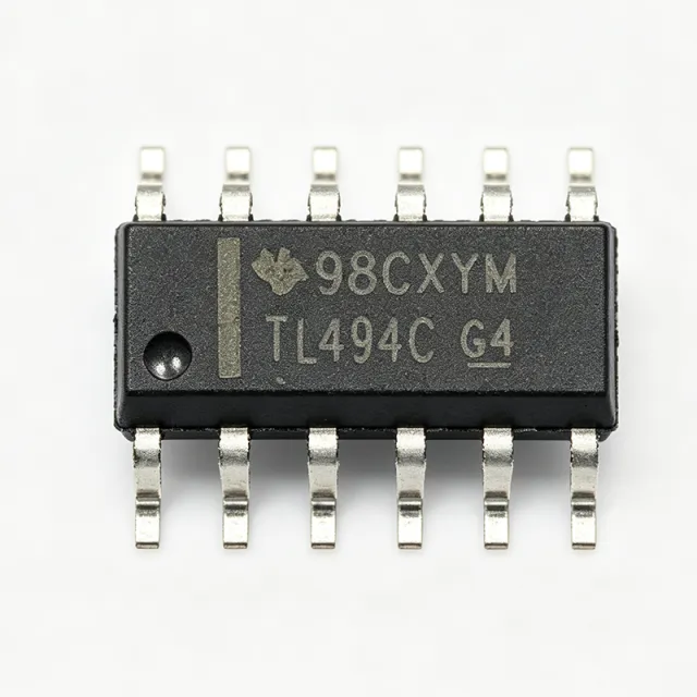
TL494CDT - PWM Controller IC | STMicroelectronics | SMPS
MPN: TL494CDT ✓ Active| Qty | Unit Price | Extended |
|---|---|---|
| 1 | $0.5455 | $0.55 |
| 10 | $0.3939 | $3.94 |
| 100 | $0.3485 | $34.85 |
| 500 | $0.3333 | $166.65 |
| 1,000 | $0.3182 | $318.20 |
TL494CDT Overview
A PWM controller is a specialized integrated circuit that generates a variable-duty-cycle square wave to regulate the output voltage of a switching power supply. It compares a feedback signal to a reference voltage and adjusts the duty cycle of the output transistors accordingly. The TL494 belongs to the family of voltage-mode PWM controllers, which are widely used in offline and DC-DC converters due to their simplicity and robustness. This category sits within the broader hierarchy of power management ICs, which also includes linear regulators, switching regulators, and battery management devices.
Key features of the TL494CDT include a complete PWM power-control circuitry, an uncommitted output for single-ended or push-pull operation, an internal oscillator with a frequency range of 1kHz to 300kHz, and a 5V reference with 5% tolerance. It also provides an error amplifier with a common-mode voltage range of -0.3V to VCC-2V, a dead-time control comparator, and a standby current of typically 6mA. These features enable precise regulation and protection in various power conversion topologies.
The TL494CDT uses a bipolar process technology, offering a proven and reliable architecture that has been in production for decades. It includes an internal 5V reference that can source up to 10mA for external use, and its output stage can sink or source up to 250mA. The device also features a shutdown control pin that can be used for overcurrent or overvoltage protection, and its dead-time control allows adjustment of the minimum off-time to prevent transformer saturation in push-pull designs.
Typical applications include switch-mode power supplies for computers, telecom equipment, industrial systems, and battery chargers. The TL494CDT is also used in DC-DC converters, inverters, and motor control circuits. Its wide supply voltage range and flexible output configuration make it a versatile choice for both single-ended and push-pull topologies.
When designing with the TL494CDT, it is important to properly set the oscillator frequency using external timing components (RT and CT) and to ensure adequate decoupling of the VCC pin. The dead-time control pin should be used to prevent shoot-through in push-pull stages, and the error amplifier compensation network must be designed for stable loop operation.
This page synthesizes distributor pricing, drop-in alternatives, and practical design notes not found in the STMicroelectronics datasheet, providing a comprehensive resource for engineers selecting a PWM controller for their power supply design.
Drop-in alternatives for TL494CDT — same package, pin-to-pin compatible. Different-package parts requiring PCB rework are excluded.
Quick Comparison Tool — Select alternative parts for side-by-side comparison:
TL594CDT
📋 Reference alternative (not in catalog)
KA7500CD
📋 Reference alternative (not in catalog)
TL494CDR
📋 Reference alternative (not in catalog)
TL494CDT Maximum Ratings & Electrical Characteristics
| Supply Voltage (VCC) | 7 V to 40 V |
| Output Current (per output) | 250 mA (sink/source) |
| Oscillator Frequency Range | 1 kHz to 300 kHz |
| Reference Voltage | 5 V ±5% |
| Reference Current | 10 mA (max) |
| Error Amplifier Common-Mode Voltage | -0.3 V to VCC-2 V |
| Dead-Time Control Range | 0% to 100% |
| Standby Current | 6 mA (typical) |
| Output Type | Single-ended or push-pull |
| Operating Temperature Range | 0°C to +70°C |
| Package | SOIC-16 (SOP-16) |
| Mounting Type | Surface Mount |
| RoHS Status | Compliant |
| MSL Level | 1 (unlimited) |
| Shutdown Pin | Yes (pin 4) |
TL494CDT Pin Configuration
| Pin 1 | 1IN+ — Non-inverting input of error amplifier 1 |
| Pin 2 | 1IN- — Inverting input of error amplifier 1 |
| Pin 3 | FB — Feedback/PWM comparator input |
| Pin 4 | DTC — Dead-time control input |
| Pin 5 | CT — Oscillator timing capacitor |
| Pin 6 | RT — Oscillator timing resistor |
| Pin 7 | GND — Ground |
| Pin 8 | C1 — Collector of output transistor 1 |
| Pin 9 | E1 — Emitter of output transistor 1 |
| Pin 10 | E2 — Emitter of output transistor 2 |
| Pin 11 | C2 — Collector of output transistor 2 |
| Pin 12 | VCC — Positive supply voltage |
| Pin 13 | OC — Output control (single-ended or push-pull) |
| Pin 14 | REF — 5V reference output |
| Pin 15 | 2IN- — Inverting input of error amplifier 2 |
| Pin 16 | 2IN+ — Non-inverting input of error amplifier 2 |
Typical Applications
TL494CDT is suitable for 6 applications: Switch-Mode Power Supplies (SMPS), DC-DC Converters, Battery Chargers, Inverters, Motor Control, Telecom Power Supplies.
Switch-Mode Power Supplies (SMPS)
The TL494CDT is a core component in switch-mode power supplies, providing PWM control for voltage regulation. Its wide supply voltage range (7V to 40V) and flexible output configuration (single-ended or push-pull) make it suitable for offline AC-DC converters and DC-DC converters. In a typical SMPS, the TL494CDT generates a PWM signal that drives a power transistor or MOSFET, which switches the input voltage across a transformer or inductor. The output voltage is sensed through a feedback network and compared to the internal 5V reference, adjusting the duty cycle to maintain regulation. The dead-time control pin prevents shoot-through in push-pull topologies, ensuring reliable operation. With an oscillator frequency up to 300kHz, the TL494CDT enables compact transformer and filter designs, reducing overall system size and cost. Its 250mA output current capability can directly drive small power stages, simplifying the driver circuitry. For higher power levels, external drivers can be added, but the TL494CDT's built-in output stage provides a cost-effective solution for many applications. The device's robust design and proven architecture make it a trusted choice for SMPS in consumer, industrial, and telecom equipment.
Recommended
DC-DC Converters
The TL494CDT is widely used in DC-DC converters for voltage step-up or step-down applications. Its internal error amplifiers and PWM comparator allow precise regulation of the output voltage. In a buck converter, the TL494CDT controls the duty cycle of a high-side switch, while in a boost converter, it controls the low-side switch. The device's 5V reference provides a stable voltage for setting the desired output level, and the dead-time control can be used to limit the maximum duty cycle, protecting the switch and inductor. The oscillator frequency can be set to optimize the trade-off between efficiency and component size; higher frequencies allow smaller inductors and capacitors but increase switching losses. The TL494CDT's 250mA output current can directly drive the gate of a power MOSFET, though a gate driver may be needed for high-current switches. Its wide input voltage range (7V to 40V) makes it suitable for automotive, industrial, and battery-powered systems. The device's low standby current (6mA) is beneficial for battery-operated equipment, extending battery life. Overall, the TL494CDT provides a flexible and reliable solution for DC-DC converter designs.
Recommended
Battery Chargers
The TL494CDT is commonly used in battery charger circuits to regulate charging current and voltage. Its error amplifiers can be configured to implement constant-current/constant-voltage (CC/CV) charging profiles, which are essential for lead-acid and lithium-ion batteries. In a typical charger, the TL494CDT senses the battery voltage and current through feedback networks and adjusts the PWM duty cycle to maintain the desired charging parameters. The device's 5V reference provides a stable voltage for setting the target voltage, while the dead-time control can be used to limit the maximum duty cycle, preventing overcharging. The wide supply voltage range allows the TL494CDT to operate from various input sources, such as AC adapters or solar panels. Its 250mA output current can directly drive a pass transistor or MOSFET in the charging path, though external drivers may be needed for high-current chargers. The device's low standby current is beneficial for maintaining battery charge without excessive power drain. The TL494CDT's robust design and thermal protection make it suitable for demanding charging applications, ensuring safe and reliable operation.
Recommended
Inverters
The TL494CDT is used in DC-AC inverters to generate PWM signals that drive the switching stage, producing a sinusoidal output. In a typical inverter, the TL494CDT operates in push-pull mode, driving two power transistors alternately to create a high-frequency AC signal, which is then filtered to produce a clean sine wave. The device's oscillator frequency can be set to a high value (e.g., 20kHz) to reduce transformer size and audible noise. The error amplifiers can be used to regulate the output voltage and current, ensuring stable operation under varying loads. The dead-time control is critical in push-pull topologies to prevent simultaneous conduction of both switches, which would cause a short circuit. The TL494CDT's 250mA output current can directly drive the gates of power MOSFETs or IGBTs, though gate drivers may be required for high-power stages. Its wide supply voltage range (7V to 40V) makes it suitable for automotive and renewable energy systems. The device's robust design and proven reliability make it a popular choice for inverter applications, from small portable inverters to larger grid-tie systems.
Recommended
Motor Control
The TL494CDT can be used in motor control circuits to regulate the speed and torque of DC motors. By varying the duty cycle of the PWM signal, the average voltage applied to the motor is controlled, thereby adjusting its speed. The device's error amplifiers can be used to implement closed-loop speed control by comparing a tachometer feedback signal to a reference voltage. The oscillator frequency can be set to a value that minimizes audible noise and motor vibration, typically in the range of 10kHz to 20kHz. The TL494CDT's 250mA output current can directly drive a power MOSFET in the motor drive circuit, though a gate driver may be needed for higher current motors. The dead-time control can be used to prevent shoot-through in H-bridge configurations, ensuring safe operation. The wide supply voltage range allows the TL494CDT to operate from various battery voltages, making it suitable for automotive, robotics, and industrial applications. Its low standby current is beneficial for battery-powered devices, extending battery life. Overall, the TL494CDT provides a cost-effective and reliable solution for motor control applications.
Recommended
Telecom Power Supplies
The TL494CDT is widely used in telecom power supplies, which require high efficiency and reliability. These power supplies typically convert AC mains or a high-voltage DC bus to the low voltages needed by telecom equipment, such as 48V or 12V. The TL494CDT provides the PWM control necessary for regulating the output voltage and current, ensuring stable operation under varying load conditions. Its wide supply voltage range (7V to 40V) allows it to be powered from the input bus or an auxiliary supply. The device's error amplifiers can be used to implement precise voltage regulation, and the dead-time control can be used to prevent transformer saturation in push-pull topologies. The oscillator frequency can be set to optimize efficiency and component size, with higher frequencies allowing smaller transformers and filters. The TL494CDT's 250mA output current can directly drive power transistors or MOSFETs, though external drivers may be needed for high-power stages. Its robust design and proven reliability make it a trusted choice for telecom power supplies, which must operate continuously in demanding environments. The device's low standby current also contributes to overall system efficiency.
Recommended
Recommended Products Summary
Engineering reference data for TL494CDT — comparison, design guidance, and compliance information.
Selection Guide
Comparison with Alternatives
| Parameter | This Product | TL594CDT | KA7500CD | TL494CDR |
|---|---|---|---|---|
| Package | SOIC-16 | SOIC-16 - same | SOIC-16 - same | SOIC-16 - same |
| Supply Voltage Range | 7V to 40V | 7V to 40V | 7V to 40V | 7V to 40V |
| Output Current (per output) | 250mA | 250mA | 250mA | 250mA |
| Reference Voltage Tolerance | ±5% | ±1% | ±5% | ±5% |
| Error Amplifier Common-Mode Range | -0.3V to VCC-2V | -0.3V to VCC-1.5V | -0.3V to VCC-2V | -0.3V to VCC-2V |
| Oscillator Frequency Range | 1kHz to 300kHz | 1kHz to 300kHz | 1kHz to 300kHz | 1kHz to 300kHz |
| Standby Current | 6mA | 6mA | 6mA | 6mA |
| Operating Temperature Range | 0°C to +70°C | 0°C to +70°C | 0°C to +70°C | 0°C to +70°C |
Key Differentiators
- Cost-effective PWM controller with proven architecture (vs TL594CDT)
- Wide supply voltage range (7V to 40V) (vs KA7500CD)
- Flexible output configuration (single-ended or push-pull) (vs TL494CDR)
Design Notes
Ensure adequate decoupling on the VCC pin (pin 12) with a 0.1uF ceramic capacitor placed as close as possible to the pin, and a 10uF electrolytic capacitor nearby. This prevents noise from the switching action from affecting the internal reference and error amplifiers, which could cause instability.
Keep the timing components (RT and CT) close to pins 5 and 6 to minimize parasitic capacitance and inductance, which can affect oscillator frequency accuracy. Use short, wide traces for high-current output paths (pins 8-11) to reduce voltage drops and EMI.
Do not leave the dead-time control pin (pin 4) floating; connect it to ground for maximum duty cycle or to a voltage divider for adjustable dead time. In push-pull mode, ensure the output control pin (pin 13) is tied to the reference (pin 14) to enable push-pull operation, and to ground for single-ended operation.
Compliance Information
RoHS compliant per STMicroelectronics product page. Not AEC-Q100 qualified. Halogen-free status not specified in provided data.






