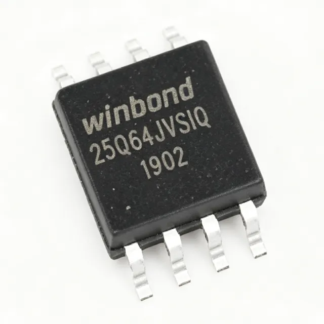
W25Q64JVSSIG - 64Mb SPI Flash 133MHz Industrial | Winbond
MPN: W25Q64JVSSIG ✓ Active| Qty | Unit Price | Extended |
|---|---|---|
| 1 | $0.45 | $0.45 |
| 10 | $0.38 | $3.80 |
| 100 | $0.3 | $30.00 |
| 500 | $0.26 | $130.00 |
| 1,000 | $0.22 | $220.00 |
W25Q64JVSSIG Overview
A serial NOR flash memory is a non-volatile storage IC that stores data in a NOR cell array and communicates over a serial peripheral interface (SPI). Unlike NAND flash, NOR flash offers random access to any address, making it the standard choice for code storage (XIP - execute in place) in embedded systems. It sits within the memory hierarchy: SPI NOR flash -> NOR flash -> flash memory -> semiconductor memory.
Key features include Quad SPI with up to 133 MHz clock (equivalent to 532 Mbps transfer), QPI (Quad Peripheral Interface) mode for faster command handling, DTR (Double Transfer Rate) support on JV variants, a 256-byte page program buffer, 4KB sectors, 32KB/64KB blocks, and hardware/software write protection. Advanced security features include individual block lock-down and a 64-bit unique ID, with the G suffix indicating Winbond's industrial-grade flow.
The device uses Winbond's proven serial flash architecture with fast erase times and low power consumption, featuring a deep power-down mode that reduces standby current to microamp levels - critical for battery-powered designs. JEDEC SFDP support simplifies second-sourcing against compatible parts.
Typical applications include embedded code storage for microcontrollers and DSPs, Wi-Fi/Bluetooth module firmware, BIOS/UEFI storage on industrial PCs, LCD/OLED display drivers, and IoT sensor nodes.
Design tip: enable the QE (Quad Enable) bit in the status register for quad operation, and verify JEDEC SFDP compatibility when second-sourcing against GigaDevice GD25Q64 parts.
This page synthesizes distributor pricing, drop-in alternatives, and practical design notes not found in the manufacturer datasheet. Pricing references are as of 2026-09-06.
Drop-in alternatives for W25Q64JVSSIG — same package, pin-to-pin compatible. Different-package parts requiring PCB rework are excluded.
Variants in this series
Same-series models that are drop-in compatible with W25Q64JVSSIG (same form factor and footprint) — differing in Interface, Memory Type, Organization, Package, Supply Voltage.
Quick Comparison Tool — Select alternative parts for side-by-side comparison:
W25Q64JVSSIQ
✅ Drop-In📋 Reference alternative (not in catalog)
W25Q64JVSSJQ
✅ Drop-In📋 Reference alternative (not in catalog)
W25Q64JVSSIM
✅ Drop-In📋 Reference alternative (not in catalog)
GD25Q64BSSIG
✅ Drop-In📋 Reference alternative (not in catalog)
MX25L6445EM2I-10G
✅ Drop-In📋 Reference alternative (not in catalog)
N25Q064A13ESEA0F
✅ Drop-In✓ In Stock
Contact for price
View Datasheet →W25Q64JVSSIG Maximum Ratings & Electrical Characteristics
| Memory Capacity | 64 M-bit (8 MB) |
| Memory Type | NOR Flash (SPI) |
| Organization | 8M x 8 |
| Interface | SPI, Dual SPI, Quad SPI, QPI |
| Maximum Clock Frequency | 133 MHz |
| Supply Voltage | 3 V to 3.6 V |
| Page Size | 256 bytes |
| Sector Size | 4 KB |
| Block Size | 32 KB / 64 KB |
| Operating Temperature | -40C to +85C (industrial) |
| Package | 8-pin SOP (SOIC-8, 208-mil) |
| Mounting Type | Surface Mount |
| Unique ID | 64-bit |
| Security Features | Individual block lock-down, hardware/software write protection |
| Standards Support | JEDEC SFDP |
| Deep Power-Down Mode | Yes (microamp standby current) |
| RoHS Status | Compliant |
W25Q64JVSSIG Pin Configuration
| Pin 1 | /CS — Chip Select (active low) |
| Pin 2 | DO (IO1) — Serial Data Output / Quad IO1 |
| Pin 3 | /WP (IO2) — Write Protect / Quad IO2 |
| Pin 4 | GND — Ground |
| Pin 5 | DI (IO0) — Serial Data Input / Quad IO0 |
| Pin 6 | CLK — Serial Clock |
| Pin 7 | /HOLD (IO3) — Hold / Quad IO3 |
| Pin 8 | VCC — Power supply, 3.0 V to 3.6 V |
Typical Applications
W25Q64JVSSIG is suitable for 6 applications: Embedded MCU Code Storage (XIP), Wi-Fi / Bluetooth Module Firmware, BIOS/UEFI Storage on Industrial PCs, IoT Sensor Nodes and Data Logging, Display Driver Configuration Storage, Network Equipment Boot and Config Storage.
Embedded MCU Code Storage (XIP)
The W25Q64JVSSIG is a natural fit for execute-in-place code storage on SPI-host microcontrollers and DSPs. Its Quad SPI interface at 133 MHz (532 Mbps equivalent) combined with fast read command 0xEB (4 dummy cycles) and continuous read mode provides the read throughput needed for memory-mapped QSPI XIP boot on ARM Cortex-M and similar cores. The 64Mb (8MB) density accommodates application code, assets, and OTA dual-bank headroom, while 4KB sectors allow fine-grained parameter storage. Because the SOP-8 footprint is standard across the W25Q family, upgrading to W25Q128 for larger firmware later requires no PCB respin.
Recommended
Wi-Fi / Bluetooth Module Firmware
Wireless modules from major vendors specify Winbond W25Q-class serial NOR for storing firmware, calibration data, and MAC parameters. The W25Q64JVSSIG's 8MB capacity covers a typical Wi-Fi SoC firmware image plus over-the-air update staging, and its QPI mode accelerates boot-time reads. The industrial -40C to +85C range and G-grade flow suit outdoor access points and industrial wireless gateways. Deep power-down mode at microamp-level standby current preserves battery budget in sensor nodes that wake periodically to transmit, and JEDEC SFDP allows host drivers to auto-configure timing without firmware changes across second sources.
Recommended
BIOS/UEFI Storage on Industrial PCs
Industrial motherboards and single-board computers use 64Mb SPI NOR for BIOS/UEFI storage, and the W25Q64JVSSIG's industrial-grade qualification (-40C to +85C, G flow) matches the reliability expectations of fanless IPCs and automation controllers. Dual/Quad SPI read performance shortens POST boot time, while hardware and software write protection plus individual block lock-down protects the boot block against corruption and unauthorized modification. The 64-bit unique ID supports platform asset tracking. Standard JEDEC SPI programmer support makes the part compatible with common BIOS flashing fixtures and in-system update flows.
Recommended
IoT Sensor Nodes and Data Logging
Battery-powered IoT nodes benefit from the W25Q64JVSSIG's low-power profile: deep power-down mode reduces standby current to microamp levels, so the flash is effectively invisible in sleep-state budgets, while active read current stays low for periodic firmware validation and data fetch. The 8MB array logs months of sensor data with 4KB sector granularity enabling wear-leveled logging. The industrial temperature range covers outdoor enclosures, and the 3.0V-3.6V rail pairs directly with 3.3V-supplied MCUs without level shifting. JEDEC SFDP support simplifies multi-vendor firmware builds when supply constraints force second sourcing.
Recommended
Display Driver Configuration Storage
LCD and OLED display modules commonly store gamma correction tables, EDID data, and driver configuration in 64Mb-class serial NOR. The W25Q64JVSSIG's fast quad reads (133 MHz clock, 532 Mbps equivalent) let display controllers fetch lookup tables quickly at power-up, minimizing visible boot delay. Its small SOP-8 footprint fits on the display board's backside, and hardware write protection (WP pin) safeguards calibration data from accidental overwrites. The industrial -40C to +85C range supports automotive-adjacent and outdoor display applications, though non-automotive qualification should be confirmed for in-vehicle use.
Recommended
Network Equipment Boot and Config Storage
Routers, switches, and industrial gateways store bootloaders, device trees, and configuration files in SPI NOR flash. The W25Q64JVSSIG provides 8MB for bootloader plus kernel staging and config logs, with QPI/DTR-capable JV architecture reducing boot latency on quad-capable SoCs. Block lock-down and write-protect features meet the integrity expectations of network infrastructure, and the industrial temperature range covers unventilated telecom cabinets. Since this is one of the highest-volume 64Mb SPI NOR parts, multi-year supply continuity is strong, and GD25Q64/MX25L6445 second sources are pre-validated by many BSP vendors.
Recommended
Recommended Products Summary
Engineering reference data for W25Q64JVSSIG — comparison, design guidance, and compliance information.
Selection Guide
Comparison with Alternatives
| Parameter | This Product | W25Q64JVSSIQ | W25Q64JVSSJQ | GD25Q64BSSIG | MX25L6445EM2I-10G | N25Q064A13ESEA0F |
|---|---|---|---|---|---|---|
| Package | SOIC-8 (SOP-8, 208-mil) | SOIC-8 - same | SOIC-8 - same | SOIC-8 - same | SOIC-8 - same | SOIC-8 - same |
| Brand | Winbond Electronics | Winbond Electronics | Winbond Electronics | GigaDevice | Macronix | Micron Technology |
| Density | 64 M-bit (8 MB) | 64 M-bit | 64 M-bit | 64 M-bit | 64 M-bit | 64 M-bit |
| Supply Voltage | 3.0 V to 3.6 V | 3.0 V to 3.6 V | 3.0 V to 3.6 V | 3.0 V to 3.6 V | 2.7 V to 3.6 V | 2.7 V to 3.6 V |
| Temperature Range | -40C to +85C (industrial) | -40C to +85C | -40C to +85C | -40C to +85C | -40C to +85C | -40C to +85C |
Key Differentiators
- 133 MHz Quad SPI with QPI mode (vs MX25L6445EM2I-10G)
- Winbond industrial-grade (G) flow (vs GD25Q64BSSIG)
- Family density scalability (vs N25Q064A13ESEA0F)
Design Notes
Place 100 nF ceramic decoupling capacitor as close as possible to the VCC (pin 8) and GND (pin 4) pins, with an additional 4.7-10 uF bulk capacitor near the flash rail. Keep SPI traces short (under 10 cm preferred) and length-match the four quad IO lines (IO0-IO3) to minimize skew at 133 MHz operation. Route CLK away from IO lines to reduce crosstalk-induced read errors, and add 22-33 ohm series resistors on CLK and data lines if signal integrity issues appear on long traces.
When the QE (Quad Enable) bit in the status register is set, the WP pin becomes IO2 and HOLD becomes IO3 - driving them low in hardware will corrupt quad transfers. Verify the QE bit state when porting firmware between W25Q64JVSSIG and second sources, since factory default QE status differs between vendors (Winbond JV parts ship QE=1 on many variants). Also confirm JEDEC SFDP tables in your driver rather than hardcoding erase timings: sector erase times can differ measurably between Winbond, GigaDevice, and Macronix parts.
Keep the supply within 3.0 V to 3.6 V at all times, including during flash program/erase when current demand peaks. If the flash shares a rail with a Wi-Fi SoC, budget for the radio's transmit burst droop - add local bulk capacitance so VCC stays above the minimum during simultaneous RF bursts and flash writes. For battery designs, actively issue the deep power-down command (0xB9) on idle; relying only on CS deassert leaves the device in standby rather than microamp-level deep power-down, wasting battery over long sleep intervals.
At 133 MHz with quad IO, the bus behaves as a transmission line on multi-layer boards with long traces. Use the fast read dummy-cycle counts from the SFDP table rather than hardcoding datasheet values - incorrect dummy cycles cause bit shifts that appear as intermittent CRC errors. If XIP execution from the flash is used, enable the continuous read mode (M7-M0 bits) to skip the 8-bit command per access, improving effective bandwidth roughly 30 percent at the same clock rate.
Compliance Information
RoHS compliant and lead-free per Winbond product positioning. Not AEC-Q100 qualified - industrial temperature range -40C to +85C only. Request REACH and conflict-minerals declarations from Winbond or distributor for formal documentation.



