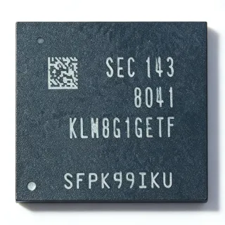
W949D2DBJX5I - 512Mb LPDDR SDRAM 200MHz x32 | Winbond
MPN: W949D2DBJX5I ✓ Active| Qty | Unit Price | Extended |
|---|---|---|
| 1 | $1.26 | $1.26 |
| 10 | $1.18 | $11.80 |
| 100 | $1.1 | $110.00 |
| 500 | $1.02 | $510.00 |
| 1,000 | $0.95 | $950.00 |
W949D2DBJX5I Overview
An LPDDR SDRAM is a mobile-optimized variant of double-data-rate synchronous DRAM. Like all DRAM, it stores each bit as charge on a capacitor that must be periodically refreshed, but LPDDR devices reduce core and I/O operating voltage and add low-power modes such as Deep Power Down and Self Refresh so that battery-powered systems can keep volatile memory alive with minimal energy. In the memory hierarchy, the W949D2DBJX5I sits as main system memory, positioned between embedded SRAM caches and non-volatile flash storage.
Key features include 512Mbit total density organized for a x32-wide parallel bus, a 200 MHz maximum clock frequency delivering effective double-data-rate transfers on both clock edges, and the space-saving 90-VFBGA 8x13 mm ball grid array that minimizes board area and improves signal integrity for high-speed memory routing. The I temperature suffix designates industrial-grade operating temperature support, and the 46nm process keeps core current low.
Technically, the device uses double data rate signaling on the DQ pins, source-synchronous data strobes (DQS) for capture, and programmable mode registers for CAS latency, burst length and burst type configuration per the LPDDR (Mobile DDR) SDRAM standard. Bank and row/column addressing follow the standard LPDDR command set with ACTIVATE, READ, WRITE, PRECHARGE, REFRESH and mode register set commands.
Typical applications include portable and industrial embedded systems: main memory for ARM-based application processors, networking and communication modules, telematics and data-loggers, and human-machine interface boards where 64 MByte of low-power DRAM is sufficient.
Design consideration: LPDDR shares command/address lines among devices, so careful length-matched routing and proper termination of the 1.8 V-class signaling environment are essential; verify the controller supports the selected CAS latency and burst configuration before layout.
This page synthesizes distributor pricing, drop-in family alternatives, pin-level guidance and practical design notes not consolidated in the manufacturer datasheet.
Drop-in alternatives for W949D2DBJX5I — same package, pin-to-pin compatible. Different-package parts requiring PCB rework are excluded.
Quick Comparison Tool — Select alternative parts for side-by-side comparison:
W949D2DBJX5E
✅ Drop-In ⚠️ 参数待验证📋 Reference alternative (not in catalog)
W949D2DBJX6I
✅ Drop-In ⚠️ 参数待验证📋 Reference alternative (not in catalog)
W949D2DBJX7I
✅ Drop-In ⚠️ 参数待验证📋 Reference alternative (not in catalog)
W949D2DBJX5I TR
✅ Drop-In📋 Reference alternative (not in catalog)
W949D2DBJX5I Maximum Ratings & Electrical Characteristics
| Memory Type | SDRAM - Mobile LPDDR (Low Power DDR SDRAM) |
| Memory Size | 512 Mbit (64 MByte) |
| Organization | x32 parallel |
| Interface | Parallel |
| Clock Frequency | 200 MHz (also supports 166 MHz grade operation) |
| Clock Cycle Time | 5 ns |
| Technology | 46nm DRAM process |
| Access Type | Double Data Rate (source-synchronous DQS) |
| Package | 90-VFBGA (8x13 mm) |
| Mounting Type | Surface Mount (BGA) |
| Refresh | Dynamic DRAM refresh (per LPDDR standard) |
W949D2DBJX5I 90-vfbga (8x13 mm) Pin Configuration Guide
Pin configuration for W949D2DBJX5I (90-vfbga (8x13 mm) package). This digital IC includes GPIO, communication interfaces (UART, SPI, I2C), and power pins. Refer to the manufacturer datasheet for alternate pin functions and configuration options. Essential for embedded system design and PCB layout.

No detailed pinout data available for W949D2DBJX5I.
Refer to the datasheet for full pin configuration.
Typical Applications
W949D2DBJX5I is suitable for 6 applications: Embedded ARM SoC Main Memory, Industrial HMI and Control Panels, Battery-Powered Data Loggers, Networking and Communication Modules, Telematics and Vehicle Data Acquisition, Smart Home and IoT Hubs.
Embedded ARM SoC Main Memory
The W949D2DBJX5I serves as main system memory for ARM Cortex-A/M application processors and embedded SoCs that expose an LPDDR (Mobile DDR) memory controller. Its 512 Mbit density in a x32 organization provides 64 MByte of volatile working memory - adequate for running embedded Linux, RTOS stacks or GUI frameworks on cost-sensitive platforms. The 200 MHz clock with double-data-rate DQ signaling delivers the bandwidth these processors expect, while source-synchronous DQS strobes maintain timing margin across the PCB. Because the core is built on a 46nm LPDDR process, standby and self-refresh currents stay low, extending battery life in portable instruments. Place the VFBGA close to the SoC with length-matched, daisy-chained routing and verify the controller's CAS latency and burst settings against the Winbond datasheet before layout.
Recommended
Industrial HMI and Control Panels
Industrial human-machine interface panels need volatile memory to buffer screen frame buffers, event logs and protocol stacks across wide ambient temperatures. The W949D2DBJX5I's I temperature grade qualifies it for industrial cabinets and factory-floor equipment where consumer-grade (E) LPDDR would be marginal. Its 90-VFBGA 8x13 mm footprint keeps the memory near the display controller without consuming board area needed for isolation and I/O circuitry. The x32 bus reduces controller complexity and part count versus x16 solutions requiring two devices for the same bandwidth. Designers should pair the device with industrial-grade PMICs for the LPDDR rail, add temperature-compensated refresh scheduling in firmware, and validate BGA solder reliability under the plant's thermal cycling profile.
Recommended
Battery-Powered Data Loggers
Portable and remote data loggers benefit from the LPDDR low-power architecture of the W949D2DBJX5I: between sampling bursts the controller can place the device in self-refresh or deep power-down, cutting standby current to microamp levels while preserving the working set. The 512 Mbit (64 MByte) capacity holds firmware heap, sensor buffering and communications stacks for cellular or LoRa loggers. Its 200 MHz, x32 interface quickly drains buffers after wake-up, minimizing the active duty cycle that dominates logger energy budgets. Industrial temperature tolerance supports outdoor enclosures. Designers should size the LPDDR supply rail for wake-up inrush, gate CKE correctly, and confirm retention-mode current figures in the Winbond datasheet for battery-life calculations.
Recommended
Networking and Communication Modules
Routers, gateways, wireless modules and industrial communication nodes use the W949D2DBJX5I as packet-buffer and main memory for network SoCs with LPDDR controllers. The x32-wide bus and 200 MHz double-data-rate operation give the throughput needed to move packets between MAC hardware and software stacks, while the 46nm core keeps the module's thermal budget small in fanless enclosures. The VFBGA package suits the dense, two-sided layouts typical of networking modules and SODIMM-style embedded cores. Because many communication SoCs implement JEDEC-standard LPDDR ball maps, board reuse across socket speeds is common - but verify speed-grade compatibility (166 MHz vs 200 MHz grades in the W949D2 family) with the SoC's memory controller timing specification before committing the BOM.
Recommended
Telematics and Vehicle Data Acquisition
Telematics units, fleet trackers and vehicle data-acquisition nodes operate over wide temperature extremes and continuous vibration, making the industrial-grade W949D2DBJX5I a fit for their main-memory pool. The 512 Mbit device buffers GPS logs, CAN traffic and cellular upload queues; self-refresh mode retains working data through ignition-off micro-sleeps that extend battery reserve. The 90-VFBGA package has a low profile and short ball interconnects that tolerate vibration better than fine-pitch TSOP alternatives, though underfill is commonly specified for automotive-adjacent environments. Engineers should confirm the I-grade temperature envelope against the vehicle cabin/engine-bay requirement, apply conformal coating and underfill per IPC assembly practice, and validate refresh behavior at the coldest ambient in system testing.
Recommended
Smart Home and IoT Hubs
Smart home hubs, security panels and IoT edge gateways combine a low-power SoC, wireless radios and the W949D2DBJX5I as working memory for protocol stacks (Zigbee, Thread, Wi-Fi bridging) and local application logic. The 64 MByte capacity comfortably hosts a lightweight Linux or RTOS image with networking services, while LPDDR low-power modes let the hub idle in an always-on-but-dormant state between events, which is critical for mains-battery-backup devices. The compact 8x13 mm VFBGA fits inside wall-mount enclosures with limited board area. Since I-grade silicon easily covers indoor ambient requirements, designers can alternatively select the E-grade family variant for cost reduction in climate-controlled deployments. Verify radio-module memory-map requirements and controller drive strength during integration.
Recommended
Recommended Products Summary
Engineering reference data for W949D2DBJX5I — comparison, design guidance, and compliance information.
Selection Guide
Comparison with Alternatives
| Parameter | This Product | W949D2DBJX5E | W949D2DBJX6I | W949D2DBJX7I | W949D2DBJX5I TR |
|---|---|---|---|---|---|
| Package | 90-VFBGA (8x13 mm) | 90-VFBGA (8x13 mm) - same | 90-VFBGA (8x13 mm) - same | 90-VFBGA (8x13 mm) - same | 90-VFBGA (8x13 mm) - same |
| Brand | Winbond Electronics | Winbond Electronics | Winbond Electronics | Winbond Electronics | Winbond Electronics |
| Memory Size | 512 Mbit | 512 Mbit | 512 Mbit | 512 Mbit | 512 Mbit |
| Organization | x32 | x32 | x32 | x32 | x32 |
| Temperature Grade | Industrial (I) | Commercial/extended (E) | Industrial (I) | Industrial (I) | Industrial (I) |
| Technology | 46nm LPDDR | 46nm LPDDR | 46nm LPDDR | 46nm LPDDR | 46nm LPDDR |
Key Differentiators
- Industrial temperature grade in the standard family (vs W949D2DBJX5E)
- Full 200 MHz speed grade (vs W949D2DBJX7I)
- Single-chip x32 bus for 64 MByte (vs W949D2DBJX5I TR)
Design Notes
LPDDR signaling is source-synchronous: route each DQS strobe with its associated DQ byte/lane as a tightly length-matched group, and length-match the differential clock pairs (CK/CK#) to the address/command bus per the Winbond datasheet skew tables. Keep the VFBGA within short escape routing of the SoC (typically under 50-75 mm) and reference traces to a solid ground plane. Estimated: maintaining intra-group skew below the datasheet tDQSS window avoids read-capture errors at 200 MHz double-data-rate operation.
Provide separate, well-decoupled VDD and VDDQ rails in the LPDDR voltage domain (nominal 1.8 V class - confirm exact ranges in the datasheet before power-tree design). Place bulk capacitance near the VFBGA power balls and at least one 0.1 uF ceramic per few supply balls. Estimated: LPDDR peak I/O currents during simultaneous bursts can transient-dip the rail; a PMIC with fast load transient response and proper sequencing of CKE/clock against power-good prevents uninitialized mode registers at power-up.
The 90-VFBGA 8x13 mm footprint requires a solder-mask-defined or non-solder-mask-defined land pattern exactly per the Winbond package drawing; do not scale it. On two- or four-layer boards, fan out via-in-pad or dog-bone escapes under the array and keep BGA reflow profile per your solder paste spec to prevent head-in-pillow defects common to large DRAM BGAs. For vibration-prone (telematics) products, specify underfill. Always cross-check the latest Winbond ball map revision before releasing the land pattern to fabrication.
Compliance Information
Compliance status was not stated in the verified web data. Modern Winbond memory products are typically RoHS compliant, but this must be confirmed on the Winbond product page or datasheet before use.