FPGA & CPLD
Produtos (6666)

XC3S50-4VQ100C - 50K Spartan-3 FPGA | AMD | 100-TQFP
The AMD/Xilinx XC3S50-4VQ100C is a 50,000-system-gate Spartan-3 field-programmable gate array with 1,728 logic cells, 63 I/O, a 1.2 V core supply, and a -4 speed grade, supplied in a 100-TQFP package. This commercial-temperature FPGA is positioned for compact, cost-sensitive embedded logic, control, and interface designs. A field-programmable gate array is a semiconductor whose logic fabric, programmable interconnect, and I/O blocks can be configured after manufacture. The XC3S50-4VQ100C belongs to the Spartan-3 FPGA family, combining configurable logic resources with dedicated digital input/output capability in a low-density package suitable for space-constrained designs. The verified device information identifies 50,000 system gates, 1,728 logic cells, 63 I/O, and a maximum stated clock frequency of 630 MHz. The -4 suffix denotes the performance grade, while VQ100 identifies the 100-pin package. The core supply is listed as 1.2 V, with an operating supply range of 1.14 V to 1.26 V and a commercial junction-temperature range of 0°C to 85°C. Unlike an application-specific integrated circuit, this FPGA permits configuration changes during development and production. That flexibility supports parallel data paths, state machines, protocol bridging, control logic, and small embedded processing systems. Its 100-pin TQFP package also exposes more general-purpose I/O than lower-density packages, although exact bank voltage, input threshold, and pin-specific capabilities require the official device documentation. Typical applications include industrial control, telecommunications support logic, consumer electronics, and compact embedded systems. The 1.2 V core makes board-level power planning important: designers should provide stable, decoupled core rails and use compatible external I/O standards according to the selected bank configuration. Tool-chain, configuration-memory, and legacy-device considerations should also be reviewed before committing a new production design. For an existing 100-TQFP Spartan-3 PCB, a replacement must be checked for exact speed grade, temperature grade, pin mapping, supply requirements, I/O standards, configuration interface, and programming-file compatibility. This page combines verified distributor specifications with practical selection, sourcing, and migration guidance rather than relying only on a catalog description.
XC3S50-4VQ100I - 50K Gate Spartan-3 FPGA | AMD
The AMD XC3S50-4VQ100I is a Spartan-3 field-programmable gate array with 50,000 system gates, 1,728 logic cells, 63 user I/Os, and a 1.2 V core supply in a 100-pin VTQFP package. The -4 suffix identifies the device speed grade, while the I suffix identifies the industrial-temperature option. Verified distributor listings identify the device as a 100-TQFP FPGA, and other supplied technical listings identify its process technology as 90 nm and maximum clocking as 630 MHz. An FPGA is a programmable semiconductor in the semiconductor and digital-logic hierarchy. Its configurable logic blocks, programmable interconnect, block RAM, and I/O resources let engineers implement parallel data paths, control logic, signal processing, and system interfaces in one device. Unlike a fixed-function application-specific integrated circuit, an FPGA can be reprogrammed during development and field updates when the architecture permits it. The XC3S50 provides 1,728 logic cells and 50,000 system gates, making it suited to compact control, interface, communications, instrumentation, and embedded-logic designs. Its 63 user I/Os provide connections for digital control, status, clocks, data buses, and serial peripherals. A 1.2 V core operating voltage reduces system power requirements, while the listed 2.5 V and 3.3 V supplies support associated I/O requirements where those supply rails are applicable to the selected configuration. The Spartan-3 architecture is intended for cost-sensitive designs that require programmable hardware without the resource level of a larger FPGA. The supplied data reports 90 nm process technology and a 630 MHz device figure, but achievable system timing remains design-dependent. External memory interfaces, clocking, constraints, I/O standards, routing congestion, and timing closure determine actual system performance rather than a single advertised device frequency. Typical uses include industrial automation, test and measurement, consumer electronics, communications control, embedded instrumentation, and general-purpose digital signal processing. Because this is an older FPGA family, engineers should confirm tool support, stock, lifecycle status, configuration-device support, and the exact pinout before beginning a new production design. The verified data does not establish whether it is currently active or discontinued. PCB design must preserve the 100-pin package footprint and exact I/O assignments. Decoupling, configuration startup, clock routing, I/O standards, and signal-integrity constraints should follow the relevant Xilinx or AMD device documentation. Do not treat the conflicting package descriptions in secondary listings as authoritative; the target is identified as a 100-pin TQFP/VTQFP device. This page combines verified distributor specifications, cross-reference findings, practical design guidance, and candid limitations. It distinguishes confirmed values from missing technical data so procurement and engineering teams can evaluate the FPGA without conflating package variants or assuming compatibility that the supplied evidence does not establish.

XC3S500E-4PQG208C - 500K Gate Spartan-3E FPGA | AMD
The AMD XC3S500E-4PQG208C is a Spartan-3E field-programmable gate array with 500,000 equivalent system gates, 10,476 logic cells, 1,164 configurable logic blocks, and 158 inputs in a 208-pin PQFP package. The device uses a 1.2 V supply and is identified by the provided data as supporting up to 572 MHz. It is a surface-mount programmable logic device for embedded control, signal processing, interface bridging, and parallel data acquisition systems. A field-programmable gate array, or FPGA, is a programmable digital logic device whose configurable logic and interconnect resources can be programmed after manufacture. FPGAs sit above fixed-function logic devices and programmable gate arrays in the digital-semiconductor hierarchy: a design can use programmable logic to implement counters, state machines, ALUs, control logic, and interface circuits without requiring a custom ASIC. Spartan-3E devices provide a practical balance between logic capacity, device cost, and design flexibility for embedded systems. The verified specifications identify the XC3S500E-4PQG208C as a 500K-gate Spartan-3E FPGA with 10,476 logic cells, 1,164 CLBs, 158 inputs, and a maximum clock frequency of 572 MHz. The 208-PQFP package provides a leaded, inspectable footprint for conventional surface-mount assembly. The C suffix and the verified distributor listings identify the exact commercial ordering code; the supplied sources do not provide a complete temperature-grade or lifecycle classification. This FPGA is suitable for control and sequencing logic where multiple parallel channels, counters, timers, and state machines must be implemented in one device. Its logic capacity can also support moderate data paths and protocol interfaces. The 572 MHz maximum clock figure should be treated as a device-level headline value; actual achievable clock rates depend on the selected I/O standard, timing constraints, routing, logic depth, and the external memory or transceiver interface. Typical applications include industrial automation, test-and-measurement front ends, communications adapters, embedded control systems, and signal-processing support. The package is particularly useful where a leaded package is preferred over a fine-pitch BGA and where the design requires a moderate number of I/O connections. Designers should verify board pinout, configuration requirements, power sequencing, I/O standards, and signal-integrity margins against the manufacturer datasheet before layout release. The principal design consideration is package-related routing and signal integrity. A 208-pin PQFP requires adequate copper clearances and controlled escape routing, especially for high-speed clock and interface nets. Configuration storage, bank supply voltages, decoupling, and pinout details must be implemented exactly as specified in the AMD Spartan-3E documentation. This page combines verified distributor and AMD documentation references with application guidance, lifecycle caveats, package-specific design notes, and explicitly qualified replacement analysis for engineers evaluating the XC3S500E-4PQG208C.

XC6SLX100-2CSG484C - 101K Logic FPGA | AMD
The AMD XC6SLX100-2CSG484C is a Spartan-6 LX family Field Programmable Gate Array (FPGA) with 101,261 logic cells, 338 user I/Os, and 4,939,776 RAM bits. The device is housed in a lead-free 484-CSPBGA (19x19 mm, 0.80 mm pitch) surface-mount package and operates from a 1.14V to 1.26V core supply. This configuration delivers a compact, high-density programmable logic solution for commercial-temperature (0C to 85C) systems. What is an FPGA? A Field Programmable Gate Array is an integrated circuit whose logic fabric can be configured after manufacturing to implement arbitrary digital functions. FPGAs sit above CPLDs in capacity and are often used for parallel processing, protocol bridging, and hardware acceleration. In a system hierarchy, the Spartan-6 LX family belongs to programmable logic devices, a subset of integrated circuits, and is widely used in communications, industrial automation, and video processing. Key features of XC6SLX100-2CSG484C include 7,911 CLBs, an internal frequency up to 667 MHz, 338 user configurable I/O pins, and 4,939,776 total block RAM bits. The -2 speed grade balances performance and power for cost-sensitive designs. The 484-ball CSPBGA package provides a 19x19 mm footprint with 0.80 mm pitch, making it suitable for space-constrained PCBs. Beneath the package, the Spartan-6 LX100 uses a 45nm CMOS process technology. This process enables high logic density and low static power, with core voltage around 1.2V. The FPGA includes dedicated clock management tile, DSP slices, and block RAM resources that can be used to build efficient digital signal processing pipelines, soft processors, and high-speed I/O interfaces. Typical applications include industrial automation controllers, telecom line cards, video and image processing, software-defined radio, and ASIC prototyping. The 338 I/O pins and abundant logic cells allow integration of multiple peripheral interfaces and custom processing engines on one device. When paired with DDR3 memory such as MT41K256M16HA-125:E or IS43TR16256AL-125KBL, the FPGA can implement high-bandwidth data buffers and packet processing. When designing with this component, plan the power delivery network carefully for the 1.14V to 1.26V core rail and respect the 0C to 85C junction temperature range. Decouple each supply pin and verify configuration memory selection before layout.

XC6SLX100-2FGG676C - 101K LEs Spartan-6 LX FPGA | AMD Xilinx
The AMD Xilinx XC6SLX100-2FGG676C is a Spartan-6 LX family Field Programmable Gate Array (FPGA) with 101,261 logic cells, 4,939,776 system gates, and 480 I/O pins, housed in a 676-ball Fine-Pitch Ball Grid Array (FBGA-676) package with 0.8 mm ball pitch and a 19×19 mm body. The -2 speed grade targets mid-range performance and is fabricated on a 45 nm CMOS process with a 1.2 V core supply; commercial temperature grade (C suffix) supports 0 °C to +85 °C operation. What is an FPGA? An FPGA (Field Programmable Gate Array) is a semiconductor device whose logic fabric, interconnect, and I/O can be reconfigured by the designer after PCB assembly. The Spartan-6 LX position in the broader hierarchy is: programmable logic -> FPGA -> low-power FPGA family. Compared with ASICs, FPGAs trade raw unit cost for design flexibility, in-system reprogrammability, and rapid prototyping, and they sit in the same tier as CPLDs and complex PLDs for glue-logic and parallel DSP workloads. Key features include 3.8 Mb of block RAM, 180 DSP48A1 slices, integrated Memory Controller Blocks (MCBs), and up to 108 Mb of embedded memory. The device supports common interfaces such as DDR, DDR2, DDR3, LVDS, LVCMOS, and PCI Express endpoint via the integrated GTP transceiver infrastructure in compatible LXT variants. The XC6SLX100 offers a balanced cost/performance ratio ideal for high-volume, cost-sensitive designs requiring substantial logic density. The LX architecture uses a 6-input LUT fabric with dedicated carry logic, distributed RAM and shift-register resources, and a multi-clock tiles structure. The internal core can run up to approximately 667 MHz depending on speed grade, and high-speed SelectIO technology provides flexible I/O support for single-ended and differential standards at data rates into the hundreds of Mbps range. Typical applications include industrial motor control, LED video walls and digital signage, surveillance IP cameras, automotive driver assistance (non-safety-critical domains), consumer video processing, and small-cell baseband processing. The Spartan-6 LX family is widely used as a bridge between CPLD and higher-density Virtex-class FPGAs. When designing with this device, plan for a 1.2 V core rail and a 2.5 V/3.3 V auxiliary supply, with I/O voltages per bank. Use Xilinx ISE Design Suite (or Vivado with legacy project import) for bitstream generation; the FBGA-676 footprint demands careful PCB stack-up and via-in-pad escape routing. This page synthesizes distributor pricing, drop-in alternatives within the Spartan-6 and competing Cyclone IV families, and practical PCB design guidance not found in a single source datasheet.
XC6SLX100-3FGG484C Spartan-6 LX FPGA 101K Cells | AMD Xilinx
The AMD Xilinx XC6SLX100-3FGG484C is a Spartan-6 LX Field Programmable Gate Array (FPGA) delivering 101,261 logic cells, 4,939,776 system gates, and 326 user I/O in a 484-ball Fine-pitch BGA package with -3 (highest performance) speed grade. An FPGA (Field Programmable Gate Array) is a semiconductor device whose logic function is defined by the customer after manufacture, rather than at the fab. FPGAs sit in the broader hierarchy of programmable logic devices (PLD) -> CPLD -> FPGA -> SoC FPGA, and combine configurable logic blocks (CLBs), programmable routing, dedicated DSP slices, Block RAM, and hardened I/O serializers. Unlike microcontrollers (which execute instructions sequentially), FPGAs perform true parallel datapath operations, making them the preferred choice for high-throughput DSP, packet processing, and custom interface bridging where latency and determinism matter more than raw CPU clock rate. The XC6SLX100-3FGG484C integrates 180 DSP48A1 slices for fixed- and floating-point acceleration, 4,824 Kbits of Block RAM, four clock management tiles (CMTs) with PLL/DLL, and SelectIO technology supporting voltages from 1.2V to 3.3V. The -3 speed grade delivers the highest Fmax in the Spartan-6 LX family, while the 45 nm process node keeps static power in the milliwatt range compared to older 90/65 nm nodes. Typical applications include high-volume consumer and industrial designs such as video processing pipelines, motor control, industrial Ethernet bridges, PCIe endpoint controllers (when paired with an external PHY), and digital signage. Designers also use it for custom packet processors in telecom backhaul equipment and as a flexible I/O expander/glue logic replacement for multiple CPLDs on a single board. When designing with the -3 speed grade, ensure your PCB footprint supports the FGG484 (Pb-free, 1.0 mm pitch, 19 x 19 mm body) BGA land pattern and provide adequate via-in-pad or microvia escape routing. Decoupling must follow the Spartan-6 PCB Design Guide for the VCCINT, VCCAUX, and VCCO rails to meet the -3 timing closure across the full industrial temperature range. This page synthesizes distributor pricing, verified drop-in same-family and cross-brand Spartan-6 equivalents, and practical board-level design guidance that is not consolidated in the manufacturer datasheet itself.
XC6SLX100T-2CSG484I - Spartan-6 FPGA 101K Logic Cells | AMD
The AMD XC6SLX100T-2CSG484I is a member of the Spartan-6 LXT FPGA family, built on a mature 45nm low-power copper process technology. It delivers 101,261 logic cells and 296 user I/O pins in a 484-ball CSBGA package, offering a balance of density, performance, and low power for high-volume applications. The device operates from a 1.2V core supply and supports a wide range of I/O standards. An FPGA (Field-Programmable Gate Array) is an integrated circuit that can be configured by the designer after manufacturing, allowing for custom digital logic implementations. FPGAs sit between ASICs and microprocessors in the design hierarchy, providing reconfigurable hardware acceleration for tasks ranging from protocol bridging to digital signal processing. The Spartan-6 family is optimized for cost-sensitive, high-volume applications where low power and system integration are critical. Key features of the XC6SLX100T-2CSG484I include 4,939,776 bits of block RAM, 268 DSP48A1 slices, and support for high-speed serial transceivers (up to 3.125 Gbps) in the LXT variant. The device also includes a hard PCI Express block, memory controllers, and advanced clock management tiles (CMTs) with PLLs and DCMs. These features enable the implementation of complete system-on-chip designs with minimal external components. From a technical perspective, the Spartan-6 family uses a 45nm process that reduces dynamic power consumption by approximately 50% compared to previous Spartan families. The fabric is based on a 6-input look-up table (LUT) architecture, providing efficient logic utilization. The device supports partial reconfiguration, allowing dynamic updates to logic functions without powering down the system. Typical applications include industrial automation, automotive infotainment, medical imaging, and communications equipment. The 296 I/O pins support various standards including LVCMOS, LVDS, and HSTL, making it suitable for interfacing with a wide range of peripherals and memory devices. When designing with this FPGA, careful attention to power supply decoupling and thermal management is essential. The 1.2V core supply should be regulated with low-noise LDOs or switching converters, and the device's power consumption should be estimated using the Xilinx Power Estimator (XPE) tool to ensure adequate cooling.

XC6SLX100T-3FGG484C - Spartan-6 FPGA 101K Logic Cells | AMD
The AMD XC6SLX100T-3FGG484C is a member of the Spartan-6 LXT family of Field Programmable Gate Arrays (FPGAs), built on a mature 45 nm low-power copper process technology. It delivers 101,261 logic cells, 296 user I/O pins, and 4,939,776 bits of block RAM, all in a 484-ball FBGA package. This device is designed for high-volume applications requiring leading system integration with the lowest total cost, offering half the power consumption of previous Spartan families and faster, more comprehensive connectivity. An FPGA (Field Programmable Gate Array) is an integrated circuit that can be configured by the customer or designer after manufacturing—hence 'field-programmable'. FPGAs are part of the broader category of programmable logic devices (PLDs), which sit between application-specific integrated circuits (ASICs) and general-purpose processors in the semiconductor hierarchy. They consist of an array of programmable logic blocks, interconnects, and I/O blocks, allowing designers to implement custom digital logic circuits without the high NRE costs of ASIC development. FPGAs are widely used in prototyping, aerospace, automotive, industrial, and communications applications where flexibility and time-to-market are critical. Key features of the XC6SLX100T-3FGG484C include 101,261 logic cells, 296 user I/O pins, 4,939,776 bits of block RAM, and support for various I/O standards including LVCMOS, LVDS, and HSTL. The device operates from a 1.2V core voltage and is available in the -3 speed grade, which is the fastest speed grade for this part. The 484-ball FBGA package measures 23x23 mm with a 1.0 mm ball pitch, providing a compact footprint for dense PCB designs. The device also includes advanced clock management tiles (CMTs) with PLLs and DCMs, and supports configuration via JTAG, SPI, and BPI interfaces. From a technical depth perspective, the Spartan-6 family is built on a 45 nm low-power copper process, which balances performance and power efficiency. The LXT variant includes high-speed serial transceivers (up to 3.125 Gbps), PCI Express endpoints, and advanced memory controllers, making it suitable for high-bandwidth applications. The device also features dedicated DSP48A1 slices for digital signal processing, providing up to 180 GMACs of performance. The -3 speed grade offers the highest performance, with maximum clock frequencies typically exceeding 400 MHz for internal logic. Typical applications for the XC6SLX100T-3FGG484C include software-defined radio (SDR), industrial motor control, medical imaging, and high-performance computing acceleration. Its combination of logic density, I/O count, and transceiver capabilities makes it ideal for bridging, protocol conversion, and real-time signal processing tasks. The device is also well-suited for aerospace and defense applications where long-term supply and traceability are required. When designing with this FPGA, careful attention must be paid to power supply decoupling and PCB layout. The core voltage (VCCINT) should be regulated at 1.2V with low-noise LDOs or switching regulators, and each power pin should have a 100 nF ceramic capacitor placed as close as possible. Additionally, the configuration bitstream must be stored in an external SPI flash or programmed via JTAG, and the device supports multi-boot for remote updates.
XC6SLX150-3FGG676C - Spartan-6 LX FPGA 147K LE | AMD Xilinx
The AMD Xilinx XC6SLX150-3FGG676C is a Spartan-6 LX family Field-Programmable Gate Array (FPGA) delivering 147,443 logic cells, 23038 Adaptive Logic Modules (ALMs), and 4,939,776 system gates in a 676-ball Fine-Pitch Ball Grid Array (FGG676) package. It carries the -3 commercial speed grade with a maximum core clock of 862 MHz, offers 498 user I/Os, and operates over the commercial 0C to +85C temperature range per the FBGA-676 27 x 27 mm, 1.0 mm pitch package profile. An FPGA (Field-Programmable Gate Array) is a type of programmable logic device (PLD) that combines logic gates, multipliers, embedded memory, and high-speed transceivers into a configurable fabric. FPGA sits in the hierarchy of programmable logic -> programmable logic device -> semiconductor -> integrated circuit. The Spartan-6 LX family targets high-volume cost-sensitive applications that demand high logic density, abundant block RAM, and integrated DSP slices without the power overhead of Virtex-class devices. By programming the LUTs, routing, and IP cores via the ISE Design Suite, engineers create custom accelerators, glue logic, video pipelines, and connectivity subsystems on a single chip. Key features of the XC6SLX150-3FGG676C include 135 Kbit distributed RAM, 4.8 Mbit block RAM, 180 DSP48A1 slices, four clock management tiles with PLL, and 498 SelectIO signals supporting LVCMOS, LVDS, and LVTTL standards. The device integrates PCI Express Endpoint blocks, GTP transceivers are NOT present on this LX variant, and supports DDR, DDR2, DDR3, and QDRII+ memory interfaces through dedicated hardware controllers. Configuration is via SPI, BPI, JTAG, or Platform Flash XCF, enabling flexible in-system reprogrammability for field upgrades. From a system-architecture perspective, the Spartan-6 LX uses a 45 nm copper CMOS process backed by an optimized core voltage of 1.14 to 1.26 V and auxiliary supply of 2.5 / 3.3 V for I/O banks. The 676-BGA package exposes 26 user I/O banks so designers can support mixed-voltage interfaces (1.2 V to 3.3 V) on a single die, ideal for bridging legacy and modern logic families in industrial control or motor-drive boards. Typical applications include industrial motor control and factory automation backbones, video surveillance processing pipelines, medical imaging front-end buffers, automotive driver-assistance pre-processing prototypes, and avionics display controllers. The combination of abundant I/O and large block RAM makes the LX150 particularly attractive for high-channel-count data acquisition and parallel sensor aggregation. When designing with this part, validate that the 676-BGA layout supports at least four routing layers with laser-drilled microvias, since 1.0 mm pitch BGA escape routes demand controlled-impedance planning. Also confirm that the ISE WebPACK license covers all required IP cores for development. This page synthesizes distributor availability, drop-in Spartan-6 family alternatives, and practical layout notes not bundled into the manufacturer datasheet.
XC6SLX150T-3FGG484I - Spartan-6 LXT FPGA 147K Logic Cells | AMD
The AMD XC6SLX150T-3FGG484I is a high-performance Field Programmable Gate Array (FPGA) from the Spartan-6 LXT family, built on a 45nm CMOS process technology. It delivers 147,443 logic cells and 23,038 adaptive logic modules (ALMs) in a 484-pin FBGA package with a 19x19 mm body and 0.80 mm pitch. The device operates from a 1.2V core supply and supports up to 296 user I/O pins, making it suitable for high-volume, cost-sensitive applications requiring substantial logic density and I/O flexibility. An FPGA (Field Programmable Gate Array) is a semiconductor device containing a matrix of configurable logic blocks (CLBs) and programmable interconnects that can be programmed after manufacturing to implement arbitrary digital logic functions. FPGAs sit within the broader hierarchy of programmable logic devices (PLDs), which themselves fall under the category of integrated circuits. Unlike fixed-function ASICs, FPGAs offer reconfigurability, enabling rapid prototyping, hardware acceleration, and in-field updates, which is critical for evolving standards and algorithm changes. Key features of the XC6SLX150T-3FGG484I include 4.71 Mbit of embedded block RAM, integrated DSP slices for signal processing, and support for multiple I/O standards including LVCMOS, LVDS, and HSTL. The -3 speed grade provides the highest performance within the Spartan-6 LXT family, with internal clock frequencies up to 667 MHz. The device also includes hardened memory controllers for DDR, DDR2, and DDR3, reducing system cost and design complexity. Technically, the Spartan-6 architecture employs a 45nm low-power copper process with a 1.2V core voltage, balancing performance and power consumption. The device integrates Clock Management Tiles (CMTs) containing DCMs and PLLs for robust clock generation and jitter filtering. The LXT variant adds high-speed serial transceivers (up to 3.125 Gbps) and PCIe endpoints, enabling advanced bridging and serial connectivity applications. Typical applications include automotive infotainment systems, industrial automation controllers, consumer electronics bridging, and high-speed data acquisition. The 296 I/Os and 4.71 Mbit memory make it ideal for video processing, motor control, and protocol conversion. The -3 speed grade ensures timing closure for demanding designs. When designing with this FPGA, careful attention to power supply decoupling is essential. Use multiple 100nF and 10uF capacitors near the VCCINT, VCCAUX, and VCCO pins to minimize noise. Additionally, configure the device's I/O standards to match the external interface voltages to prevent damage and ensure signal integrity.
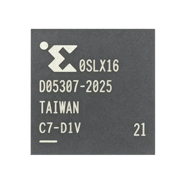
XC6SLX16-2CPG196I - 14k Logic Cells Spartan-6 FPGA | AMD
The AMD (Xilinx) XC6SLX16-2CPG196I is a Spartan-6 LX FPGA built on a 45 nm CMOS process, delivering 14,579 logic cells with 106 user I/Os in a 196-ball 8 mm × 8 mm CSBGA (TFBGA) package, with 576 Kbit of embedded block RAM and integrated DSP slices. The “-2” speed grade and industrial-grade (-40 °C to +100 °C) “I” temperature suffix indicate a -2 speed/performance tier intended for industrial-temperature environments. A Field Programmable Gate Array (FPGA) is a semiconductor integrated circuit built from configurable logic blocks (CLBs), programmable routing, and dedicated hardware resources such as block RAM, multipliers/DSP slices, and clock management tiles (DCMs/PLLs). The Spartan-6 LX series sits in the low-power, low-cost tier of the AMD/Xilinx product hierarchy: FPGA -> programmable logic -> logic IC -> integrated circuit. Spartan-6 LX devices target high-volume, cost-sensitive bridging, control, and signal-processing applications that need the parallelism and reconfigurability of an FPGA without the cost of a Virtex-class device. Key features of the XC6SLX16-2CPG196I include: 14,579 logic cells (~2,300 logic slices), 106 maximum user I/Os (some version/board use this number; package allows up to 106), 576 Kbit (72 Kbyte) of block RAM, 32 DSP48A1 slices, four DCMs and two PLLs for clock management, on-chip memory controllers (MCB) for DDR/DDR2/LPDDR, and a 1.2 V core supply with dedicated high-performance/low-power transceiverless I/O banks. The device is implemented on 45 nm process technology, delivering low static and dynamic power versus previous Spartan generations. The -2 speed grade is the mid-tier in the Spartan-6 family and balances Fmax and power for typical industrial designs. Architecturally, the XC6SLX16-2CPG196I uses a register-rich, columnar LUT-6 architecture with dedicated carry chains, distributed RAM/SRL16 shift-register logic in each CLB, and a hard PCIe endpoint block on higher-density siblings (note: LX16 does not include the integrated PCIe block; it is on LX45+). Multiple I/O standards (LVCMOS, LVDS, HSTL, SSTL) are supported with per-bank reference voltages, and the package is lead-free (Pb-free) RoHS-compliant. The 8 × 8 mm CSBGA package supports high-density board layouts in space-constrained designs. Typical applications include industrial motor control and factory automation, automotive infotainment displays and driver-assistance modules, consumer video bridging (HDMI/LVDS), low-cost software-defined radio front-ends, embedded vision pre-processing, and communication backplane bridging. The 576 Kbit of block RAM and 32 DSP slices make the LX16 well suited to small FIR/IIR filters, modest FFT engines, sensor-fusion pre-processing, and glue-logic aggregation. Pairing with a small external SPI flash for configuration memory keeps the BOM lean. When designing with this FPGA, verify that the -2 speed grade meets your target Fmax for the design floorplan, ensure JTAG and DONE pull-up values match the Spartan-6 configuration user guide, and check I/O-bank voltage compatibility before mixing 3.3 V peripherals with 1.2 V core logic. Note: the LX16 does not include the integrated PCIe block; use LX45/LX75/LX100/LX150 if PCIe hard IP is required. This page synthesizes AMD/Xilinx datasheet specifications, distributor pricing as of 2026-10-11, same-package drop-in alternatives within the Spartan-6 family, and practical design notes.

XC6SLX16-2CSG324C - 14,579-Cell Spartan-6 LX FPGA | AMD
AMD XC6SLX16-2CSG324C is a Spartan-6 LX field-programmable gate array built on a 45 nm process, with 14,579 FPGA cells, 232 I/Os, a -2 speed grade, and a 324-LFBGA package. The device combines programmable logic, block RAM, and DSP resources in a single integrated circuit for compact digital control, signal-processing, communications, and industrial automation designs. Its stated internal frequency is 667 MHz, while its nominal supply voltage is 1.2 V. A field-programmable gate array, or FPGA, is a reconfigurable semiconductor that lets engineers implement digital logic functions through programmable configuration rather than a fixed mask set. Within the broader semiconductor hierarchy, an FPGA is a programmable digital logic device that sits alongside microcontrollers, DSPs, and ASICs. It is useful when a design needs parallel hardware, adaptable interfaces, or logic that can be updated after manufacture. The Spartan-6 LX family combines configurable logic blocks with dedicated block RAM and DSP48 processing resources. The verified product listing identifies 232 I/Os and 14,579 cells, providing a substantial logic surface for control planes, data acquisition, protocol bridges, and embedded signal-processing functions. The -2 suffix denotes the device speed grade, while the CSG324 ordering code identifies the specific 324-ball package variant used by the manufacturer. The supplied data describes the device as a lead-free 19 mm by 19 mm package with 0.80 mm pitch. One retrieved specification identifies the physical description as CSBGA-484, while the distributor listing identifies the orderable package as 324-LFBGA/CSPBGA; these package descriptions require confirmation against the official ordering information before footprint release. The stated operating temperature range is 0°C to 85°C for the version described by the retrieved datasheet source. Typical applications include industrial automation, bridging, communications, consumer equipment, and control systems where programmable logic and parallel I/O are valuable. An FPGA can implement multiple interfaces concurrently, while its configurable architecture allows design revisions without changing the physical device. Compared with a fixed-function ASIC, this flexibility is useful for prototypes and evolving systems, although FPGA power, clocking, and configuration requirements must be considered during design. A key design consideration is confirming the exact package, ball map, voltage requirements, configuration interface, memory resources, and I/O standards against the official AMD Spartan-6 documentation before layout or replacement qualification. This page consolidates verified distributor metadata, pricing references, package information, and drop-in replacement guidance while clearly identifying values that still require manufacturer confirmation. This information is intended for design comparison and sourcing support rather than certification. Spartan-6 LX devices in a common supported package may be pinout compatible, but engineers must verify the specific speed grade, temperature grade, device variant, package, and intended operating conditions before substitution.
XC6SLX16-2FT256I - Spartan-6 LX FPGA, 14K LCs, 256-BGA | AMD
The AMD (formerly Xilinx) XC6SLX16-2FT256I is a Spartan-6 LX family Field Programmable Gate Array (FPGA) with 14,579 logic cells, 589,824 bits of block RAM, and 186 user I/O, housed in a 256-ball Fine-Pitch Thin Ball Grid Array (FTBGA-256) package with industrial-grade -40C to +100C temperature rating and -2 speed grade performance. An FPGA (Field Programmable Gate Array) is a semiconductor integrated circuit composed of configurable logic blocks (CLBs), programmable interconnect, and dedicated silicon IP such as block RAM, DSP slices, and clock management tiles (CMTs). FPGAs occupy a position between general-purpose microcontrollers (software-defined behavior, sequential execution) and application-specific integrated circuits (ASICs, fixed function, highest performance per watt). The Spartan-6 family specifically targets cost-sensitive, high-volume applications where ASIC NRE costs are prohibitive but microcontroller performance is insufficient. Key features of the XC6SLX16-2FT256I include 2,278 Kbits total block RAM, 32 DSP48A1 slices for fixed-point and signal-processing arithmetic, four clock management tiles (CMTs) with digital clock managers (DCMs) and phase-locked loops (PLLs), and integrated SelectIO technology supporting single-ended and differential I/O standards up to 1080 Mbps. The device is fabricated on a 45 nm CMOS process and operates from a 1.2 V core supply with separate I/O bank voltages from 1.2 V to 3.3 V. Architecturally, the Spartan-6 LX family uses a 6-input LUT-based logic fabric with dedicated carry chains, distributed SRL16/SRL32 shift-register primitives, and a 16-bit block RAM/FIFO controller per BRAM tile. The 256-ball FTBGA package provides 186 effective user I/O after accounting for power, ground, configuration, and dedicated JTAG pins. Typical applications include industrial motor control, video processing pipelines, low-cost software-defined radio, LED video wall controllers, and embedded vision pre-processing. The 256-BGA package suits designs requiring dense I/O and moderate thermal dissipation. When designing with this device, ensure proper decoupling with 100 nF ceramic capacitors at every supply pin and a 4.7-10 uF bulk capacitor near the core rail. Configuration can be sourced from SPI flash, JTAG, or BPI parallel memory; the dedicated DONE and INIT_B pins must be monitored for proper startup sequencing. This page synthesizes distributor pricing, verified drop-in alternatives, and practical design notes not found in the manufacturer datasheet alone.
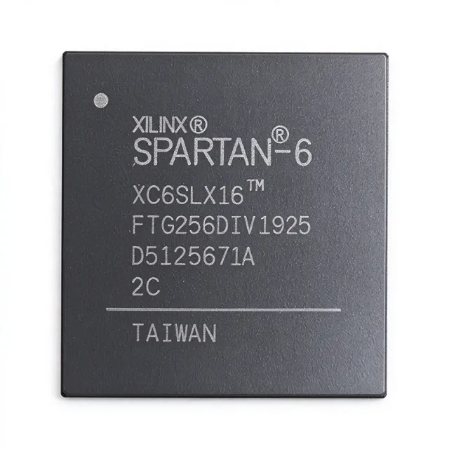
XC6SLX16-2FTG256C - Spartan-6 LX FPGA, 14K Cells, 256-BGA
The AMD (Xilinx) XC6SLX16-2FTG256C is a member of the Spartan-6 LX family of field-programmable gate arrays (FPGAs) providing 14,579 logic cells (approximately 1,139 CLBs), 589,824 bits of block RAM, and 186 maximum user I/Os in a 256-ball fine-pitch thin BGA (FTG256) package. Built on a 45 nm CMOS process, the LX variant targets low-cost, high-volume applications with an emphasis on logic density and embedded memory, while delivering typical core performance up to 667 MHz. FPGAs are programmable logic devices that allow hardware designers to implement arbitrary digital circuits, ranging from glue logic and bus bridges to full processor subsystems and DSP pipelines. The Spartan-6 LX series specifically targets cost-sensitive, high-volume designs such as consumer electronics, industrial control, automotive infotainment, and communications infrastructure. Within the broader taxonomy, FPGAs sit alongside CPLDs (less-dense, non-volatile), ASICs (fixed-function, high-volume), and microcontrollers (software-programmed sequential); FPGAs uniquely offer hardware-level parallelism with reconfigurable logic. Key features of the XC6SLX16 include the 256-ball FTG256 package at 1.0 mm ball pitch, a 17×17 mm body, lead-free/RoHS-compliant construction, and an industrial-class (-2) speed grade. The device integrates dual 10/100/1000 Ethernet MACs, dedicated DSP slices (32 of them, totaling 8.18 GMAC/s when fully packed), and 32 BRAM blocks supporting 18 Kb each. Configuration is supported through JTAG (IEEE 1149.1/1532), SPI (x1, x2, x4), and BPI (x8, x16) modes, while clock management is handled by up to 4 clock management tiles (CMTs) containing mixed-mode clock managers and PLLs. Typical applications include high-volume bridging between legacy video or memory interfaces and modern SoCs, motor control loops, low-cost industrial Ethernet endpoints, video processing pipelines, and embedded soft-processor cores such as MicroBlaze or PicoBlaze. Designers frequently pair the Spartan-6 LX with companion DDR memory controllers and high-speed serial transceivers (where required by the chosen package). A critical design consideration with the XC6SLX16-2FTG256C is its lifecycle status: the Spartan-6 family is generally considered NRND (Not Recommended for New Designs) per AMD/Xilinx's product longevity notice. Engineers building production hardware should evaluate Artix-7 or Spartan-7 successors for new projects while keeping this part viable for maintenance of legacy designs. Power decoupling, multi-bank I/O voltage referencing, and bitstream encryption (AES-256) also require careful PCB and firmware planning. This page synthesizes authorized distributor pricing, same-package drop-in alternatives, and practical hardware-design guidance that goes beyond the datasheet's typical-application notes — including lifecycle awareness for engineers managing long-life industrial installations.

XC6SLX16-3CPG196C - Spartan-6 LX FPGA 14579 Cells 106 I/O | AMD
The AMD (Xilinx) XC6SLX16-3CPG196C is a Spartan-6 LX family Field Programmable Gate Array delivering 14,579 cells, 1,451 Kbits of block RAM, and 106 user I/O in a 196-ball CSBGA (0.5 mm pitch, 8x8 mm) package. The device operates at the -3 speed grade, the highest performance bin in the Spartan-6 LX series, with a maximum internal clock frequency of 667 MHz and 1.2 V core supply. An FPGA (Field Programmable Gate Array) is a reprogrammable semiconductor that combines configurable logic blocks, programmable interconnect, and dedicated silicon resources such as block RAM, DSP slices, and clock managers. FPGAs sit between general-purpose microcontrollers and fixed-function ASICs in the digital-logic hierarchy: they deliver ASIC-level performance and parallelism while remaining reprogrammable in the field. The Spartan-6 family specifically targets cost-sensitive, high-volume applications where power consumption, density, and price-per-logic-cell are critical. Key features of the XC6SLX16-3CPG196C include 14,579 logic cells, 1,451 Kbits of block RAM (576 Kbits dual-port), 32 DSP48A1 slices, 2 clock management tiles (CMTs), and 2 PCIe hard IP blocks. The 106 available user I/Os support multiple I/O standards including LVCMOS, LVDS, and LVTTL at programmable slew rates and strengths. The CSBGA-196 package (8x8 mm body, 0.5 mm ball pitch) suits compact, high-density PCB layouts. The Spartan-6 LX architecture is built on a 45 nm CMOS process and provides lower static and dynamic power than the prior Spartan-3A generation. The device integrates a hard PCIe endpoint block (1-lane Gen1), hard memory controllers for DDR/DDR2/DDR3/LPDDR, and a high-speed GTP serial transceiver-free design (the LX family omits transceivers, unlike the LXT). The -3 speed grade delivers the highest Fmax in the family. Typical applications include industrial motor and motion control, video surveillance and image processing, low-cost PCIe endpoint cards, consumer display controllers, and embedded DSP systems. The CSBGA-196 footprint is particularly suitable for space-constrained designs such as portable test equipment and 4-layer FR4 carrier boards. The 45 nm process and 1.2 V core reduce thermal dissipation compared to older 90 nm and 65 nm FPGA families. When designing with this device, allocate sufficient decoupling capacitance (typically 100 nF and 4.7 uF combinations) at each supply pin and follow AMD's Spartan-6 PCB Design Guide for controlled-impedance routing. The 0.5 mm pitch CSBGA requires via-in-pad or laser-drilled microvia technology on standard 4-layer boards; ensure your PCB fabrication process supports the pitch before committing to layout.

XC6SLX16-3FTG256C - Spartan-6 LX FPGA, 14k LCs, 256-FTBGA | AMD
The AMD (formerly Xilinx) XC6SLX16-3FTG256C is a Spartan-6 LX field-programmable gate array (FPGA) providing 14,579 logic cells, 186 maximum user I/Os, and 256 Kbits of distributed RAM in a 256-ball fine-pitch thin-ball grid array (FTBGA-256, 17 x 17 mm, 1.0 mm pitch). It uses 45 nm CMOS process technology and operates from a 1.2 V core supply with multi-voltage I/O support. An FPGA (Field-Programmable Gate Array) is a programmable logic device that lets engineers implement arbitrary digital circuits using configurable logic blocks (CLBs), programmable I/Os, on-chip memory, and dedicated hard IP such as transceivers, DSP slices, and clock management tiles. FPGAs are part of the programmable logic hierarchy alongside CPLDs and sit between discrete logic and ASICs in system design trade-offs. The XC6SLX16-3FTG256C features 1139 CLBs, 32 DSP48A1 slices, two clock management tiles (CMTs) with mixed-mode clock managers (MMCMs) and PLLs, and SelectIO high-performance I/O supporting LVDS, LVCMOS, LVTTL, SSTL, and HSTL standards across 8 I/O banks. The -3 speed grade targets high-performance designs with up to 667 MHz internal clocking. Typical applications include industrial motor control, video processing pipelines, automotive driver assistance, low-cost wireline aggregation, and embedded control systems. Its small 17 x 17 mm BGA footprint suits cost-sensitive high-volume designs. Design tips: pay careful attention to the banked I/O supply pins (VCCO), keep the auxiliary supply VCCAUX at 2.5 V to 3.3 V, and use the -C commercial temperature grade (0 C to +85 C) only inside chassis environments. This page aggregates DigiKey/Mouser distributor pricing, same-footprint alternatives in the Spartan-6 family, and 45 nm power-rail guidance not found in the manufacturer datasheet.
XC6SLX16-3FTG256I - Spartan-6 LX FPGA, 14K Logic Cells, 256-FTBGA | AMD Xilinx
The AMD Xilinx XC6SLX16-3FTG256I is a Spartan-6 LX field-programmable gate array (FPGA) integrating 14,579 logic cells (1,139 Configurable Logic Blocks), 589,824 bits of block RAM, and 186 user I/O into a 256-ball fine-pitch thin-ball grid array (FTBGA, 17 x 17 mm, 1.0 mm pitch) package, qualified to the industrial temperature range (-40C to +100C). It belongs to the -3 speed grade, the highest performance tier within the Spartan-6 LX family, and is fabricated on a 45 nm CMOS process that lowers static power relative to earlier 65 nm Spartan generations while preserving the 667 MHz internal operation supported by the silicon. A field-programmable gate array (FPGA) is a semiconductor device built from an array of programmable logic blocks, programmable interconnect, programmable I/O cells, and dedicated hard IP such as block RAM, DSP slices, and clock management tiles. Within the broader taxonomy it sits alongside CPLDs, gate arrays, and ASICs as a re-programmable digital logic device; FPGAs differ from CPLDs mainly in density and architectural granularity, and differ from ASICs by being configurable post-fabrication. The Spartan-6 LX family is positioned by AMD Xilinx as the cost-optimized, low-power member of the Spartan-6 generation, ideal for bridging, display, and motor-control in ASICs and ASSPs. Key features include integrated block RAM up to 589,824 bits, dual 10/100/1000 Mbps Ethernet MAC hardening options, a low-power 45 nm process with 1.2 V core voltage, integrated PCI Express endpoint block in LXT variants, and a programmable I/O voltage range that supports common single-ended and differential standards. The CLB array contains 1,139 logic cells arranged to deliver balanced logic, memory, and DSP resources, and the package's fine-pitch BGA delivers compact board area while keeping signal integrity manageable for the supported I/O rates. Spartan-6 LX uses the proven 45 nm CMOS process and the 6th-generation Xilinx FPGA architecture, bringing logic, block RAM, DSP48A1 slices, and clock management tiles (CMT) into a low-cost fabric. Memory controllers (hard MCBs) support DDR, DDR2, DDR3, and LPDDR external memory interfaces up to 800 Mb/s data rates, and the integrated GTP serial transceivers in LXT parts deliver multi-gigabit connectivity for cost-sensitive serial links. Typical applications for the XC6SLX16-3FTG256I include industrial motor-control and PLC backplanes, low-cost video bridging and consumer display controllers, automotive infotainment and telematics subsystems, machine-vision front ends, and PCIe endpoint cards in cost-sensitive computing. The wide industrial temperature range and high I/O count make it a frequent building block in factory automation and embedded vision designs. When designing with this FPGA, ensure that the I/O bank voltages reference the classfree reference design, ensure that the configuration memory (typically a SPI or BPI flash) is sized for the bitstream, and ensure that the FPGA's power-on sequencing and decoupling network match the Spartan-6 power distribution guidance in UG393 to ensure reliable industrial-temperature operation. Designers should also budget for ISE Design Suite or Vivado (legacy) toolchain support and the appropriate license. This page synthesizes distributor pricing, drop-in alternatives, and practical design notes not found in the manufacturer datasheet, giving engineers an at-a-glance view of where the XC6SLX16-3FTG256I fits in the Spartan-6 LX family and what alternatives exist for sourcing continuity.
XC6SLX25-2FGG484I - Spartan-6 FPGA 24051 Cells | AMD
The AMD XC6SLX25-2FGG484I is a Field Programmable Gate Array (FPGA) from the Spartan-6 LX family, built on a mature 45 nm low-power copper process technology. It delivers 24,051 logic cells, 958,464 bits of block RAM, and 266 user I/O pins in a 484-ball FBGA package (23x23 mm, 1 mm pitch). The device operates at a core voltage of 1.2V and supports internal clock frequencies up to 500 MHz, with a -2 speed grade providing a balanced performance-power trade-off. An FPGA is an integrated circuit that can be programmed after manufacturing to implement any digital logic function. FPGAs belong to the programmable logic device (PLD) family, which sits between ASICs and general-purpose processors in the semiconductor hierarchy. They offer reconfigurability, parallel processing, and low non-recurring engineering costs, making them ideal for prototyping, low-to-mid volume production, and applications requiring hardware flexibility. Key features of the XC6SLX25-2FGG484I include 24,051 logic cells, 52 DSP48A1 slices, 958,464 bits of block RAM, and support for multiple I/O standards including LVCMOS, LVDS, and SSTL. The device also features integrated memory controllers, clock management tiles (CMT) with PLL and DCM, and support for PCI Express (in LXT variants). The -2 speed grade offers a balance between performance and power consumption, with a maximum internal frequency of 500 MHz. The Spartan-6 family is designed for high-volume, cost-sensitive applications, offering half the power consumption of previous Spartan families. The 45 nm process technology enables high logic density and low static power. The device includes advanced power management features such as suspend mode and partial reconfiguration support, allowing dynamic power optimization in battery-powered systems. Typical applications include industrial automation, automotive infotainment, medical imaging, communications infrastructure, and video processing. The 484-ball FBGA package provides ample I/O for interfacing with external memory, ADCs, DACs, and high-speed serial transceivers (in LXT variants). The industrial temperature grade (-40°C to +100°C) makes it suitable for harsh environments. When designing with this FPGA, ensure proper decoupling of the 1.2V core supply and 2.5V/3.3V auxiliary supplies. Use the configuration pins (MODE, DONE, PROG_B) for reliable device programming. The device supports multiple configuration modes including Master SPI, Slave SelectMAP, and JTAG, providing flexibility in system design.
XC6SLX25-2FT256I - Spartan-6 LX FPGA, 24K Logic Cells | AMD
The AMD (formerly Xilinx) XC6SLX25-2FT256I is a Spartan-6 LX Field-Programmable Gate Array (FPGA) integrating 24,051 logic cells, 1,879 Configurable Logic Blocks (CLBs), and 958 Kbits of block RAM in a 256-ball Fine-Pitch Thin Ball Grid Array (FTBGA-256) package. It is built on a 45 nm CMOS process, supports up to 186 user I/O, and runs at internal frequencies up to 500 MHz in this -2 (standard performance) and -I (industrial temperature, -40C to +100C) grade. A Field-Programmable Gate Array (FPGA) is a semiconductor device built around an array of configurable logic blocks (CLBs), programmable interconnect, and dedicated silicon resources such as block RAM, DSP slices, and clock-management tiles (CMTs). FPGAs occupy the middle ground between fixed-function ASICs and software-driven microcontrollers: they deliver ASIC-class parallelism and data-path throughput while remaining fully re-programmable in the field. The Spartan-6 LX family is positioned at the low-cost, low-power end of the AMD/Xilinx FPGA portfolio and is widely used in bridging, motor control, video processing, and industrial automation. Key features of the XC6SLX25-2FT256I include 24,051 logic cells, 1,879 CLBs, 4,824 Kbits of distributed RAM, 38 DSP48A1 slices running up to 390 MHz, 2 CMTs for PLL-based clock management, and a 32-bit MultiBoot configuration controller. Industrial temperature grade -I supports -40C to +100C operation. The FT256 package provides 186 user I/O across 256 balls with 1.0 mm pitch and 17 x 17 mm body. The -2 speed grade offers the standard balance of performance and power consumption for cost-sensitive embedded designs. The architecture pairs 6-input Look-Up Tables (LUT6) with dual flip-flops per slice, enabling efficient state-machine and pipelined datapath implementations. The Memory Controller Block (MCB) supports DDR, DDR2, DDR3, and LPDDR external memories at up to 800 Mb/s, while the SelectIO technology supports voltages from 1.2 V to 3.3 V on the same bank. Typical applications include industrial control and bridging, automotive infotainment head units, motor and servo drive feedback, low-cost video processing, custom glue logic replacement, and consumer electronics requiring low-power parallel DSP. The wide temperature grade also makes it suitable for factory automation and outdoor display systems. When designing with this part, note that Spartan-6 FPGAs require a separate configuration memory or JTAG programming interface; the device does not boot from internal flash. Plan the bank I/O voltage ahead of placement to avoid level-shifter overhead. This page consolidates distributor pricing for the AMD XC6SLX25-2FT256I, drop-in FT256 Spartan-6 variants, and practical design notes that go beyond the manufacturer datasheet summary.
XC6SLX25-3FGG484I - Spartan-6 FPGA 24051 Cells | AMD
The AMD XC6SLX25-3FGG484I is a member of the Spartan-6 LX family of Field Programmable Gate Arrays (FPGAs), fabricated using a 45nm CMOS process technology. It features 24,051 logic cells, 1,879 configurable logic blocks (CLBs), and 958,464 total RAM bits, providing a balanced mix of logic density and memory resources for a wide range of digital designs. The device is offered in a 484-ball FBGA package (23x23 mm) with 266 user I/O pins, supporting diverse interface standards and flexible I/O configurations. An FPGA (Field Programmable Gate Array) is an integrated circuit that can be configured by the designer after manufacturing, allowing for custom digital logic implementation. FPGAs belong to the programmable logic device (PLD) family, which sits between fixed-function ASICs and general-purpose processors in terms of flexibility and performance. The Spartan-6 series is optimized for low power and cost-sensitive applications, making it a popular choice for industrial, automotive, and telecommunications systems. Key features of the XC6SLX25-3FGG484I include a speed grade of -3, which is the highest performance grade available for Spartan-6 LX devices, enabling faster clock frequencies and improved timing margins. The device operates from a 1.2V core supply (1.14V to 1.26V range) and supports multiple I/O standards, including LVCMOS, LVDS, and HSTL. It also includes dedicated DSP48A1 slices and block RAM for efficient implementation of arithmetic and memory-intensive functions. From a technical perspective, the Spartan-6 architecture incorporates a 6-input look-up table (LUT) fabric, advanced clock management tiles (CMTs) with PLLs and DCMs, and high-speed serial transceivers (in LXT variants). The -3 speed grade provides a maximum internal frequency of 500 MHz, as noted in the datasheet, enabling high-throughput designs. The device is RoHS compliant and lead-free, meeting modern environmental standards. Typical applications for the XC6SLX25-3FGG484I include industrial automation, telecommunications infrastructure, automotive electronics, and video/image processing. Its combination of logic density, I/O count, and low power consumption makes it suitable for bridging, protocol conversion, and real-time control tasks. When designing with this FPGA, careful attention must be paid to power supply decoupling and PCB layout to ensure signal integrity at high speeds. The device requires multiple supply rails (VCCINT, VCCAUX, VCCO) and proper sequencing during power-up. Refer to the Spartan-6 FPGA datasheet and PCB design guidelines for detailed recommendations.
XC6SLX25-N3CSG324C - Spartan-6 FPGA, 24051 Cells | AMD
The AMD XC6SLX25-N3CSG324C is a member of the Spartan-6 LX family of Field Programmable Gate Arrays (FPGAs), designed for high-volume, cost-sensitive applications that require leading system integration capabilities. This device features 24,051 logic cells, 226 user I/O pins, and 958,464 total RAM bits, all housed in a 324-ball CSBGA (Chip-Scale Ball Grid Array) package. Operating from a 1.2V core supply, the XC6SLX25-N3CSG324C is fabricated using a 45nm process technology, balancing performance with power efficiency. An FPGA (Field Programmable Gate Array) is an integrated circuit that can be programmed after manufacturing to implement any digital logic function. FPGAs consist of configurable logic blocks (CLBs), programmable interconnects, and I/O blocks, allowing designers to create custom hardware without the cost and lead time of ASIC development. The Spartan-6 family sits within the broader FPGA hierarchy, positioned as a cost-optimized line below the higher-performance Virtex and Kintex families, making it ideal for applications where price and power are critical. Key features of the XC6SLX25-N3CSG324C include 1,879 CLBs, 38 DSP48A1 slices for digital signal processing, and support for a wide range of I/O standards through SelectIO technology. The device also includes enhanced mixed-mode clock management (MMCM) blocks for precise clock generation, and supports configuration via JTAG, SPI, and BPI interfaces. With a junction temperature range of 0°C to 85°C, this commercial-grade FPGA is suitable for typical industrial and consumer environments. The Spartan-6 architecture incorporates advanced power management modes, including suspend and hibernate states, to reduce static power consumption. The 45nm process technology enables high logic density while maintaining low dynamic power, making the XC6SLX25-N3CSG324C an energy-efficient choice for battery-powered or thermally constrained designs. Additionally, the device supports AES bitstream encryption and Device DNA protection for enhanced IP security. Typical applications for the XC6SLX25-N3CSG324C include motor control, industrial networking, video processing, and software-defined radio. Its 226 I/O pins and 324-ball package provide ample connectivity for interfacing with sensors, ADCs, DACs, and communication transceivers. The FPGA's reconfigurability allows for rapid prototyping and field updates, reducing time-to-market. When designing with this FPGA, careful attention must be paid to power supply decoupling and PCB layout to ensure signal integrity at high I/O speeds. The device requires a 1.2V core supply and 2.5V/3.3V auxiliary supplies, with proper sequencing as specified in the datasheet. Thermal management is also important, as the CSBGA package has a thermal resistance that must be considered for high-utilization designs.
XC6SLX4-2CPG196C - 3,840-Cell Spartan-6 FPGA | AMD
The AMD XC6SLX4-2CPG196C is a Spartan-6 LX field-programmable gate array with 3,840 logic cells, 106 I/O, 196 CSBGA balls, and 45 nm CMOS technology in a 1.2 V device. It is packaged as a 196-TFBGA/CSBGA and is identified by the -2 speed grade and C commercial temperature designation. The device also provides 221,184 registers and 216 Kb block RAM according to the verified product search data. A field-programmable gate array, or FPGA, is a programmable digital semiconductor in which logic, memory, and I/O behavior are configured through a bitstream after manufacture. The Spartan-6 LX FPGA family is intended for compact embedded systems requiring deterministic parallel logic, programmable I/O, and moderate on-chip memory. The XC6SLX4-2CPG196C therefore sits between fixed-function logic and higher-capacity programmable-logic devices. The verified data identifies the part as a Spartan-6 LX FPGA with 106 I/O, 3,840 logic cells, 196-CSBGA packaging, 1.2 V operation, and 45 nm CMOS technology. The device also includes 8 DSP slices and up to 3.2 Gbps transceiver performance in the supplied comparison source. These characteristics make it suitable for embedded control, industrial automation, communications, instrumentation, and compact signal-processing designs. The -2 suffix is a speed-grade designation, while the C suffix identifies the commercial temperature option according to the part naming convention reflected in the search results. The 196-CSBGA package provides a high ball count for dense I/O and power distribution, but it requires careful PCB layout, via-in-pad or escape routing strategies, and thermal planning. Configuration, programming, and tool support must be checked against the selected system design before releasing a production layout. For new designs, engineers should verify the complete pinout, supported I/O standards, configuration requirements, and power-supply sequencing in the manufacturer datasheet. The BGA package makes fanout and assembly inspection more demanding than a leaded package, so PCB fabrication and assembly capability should be confirmed early. This page consolidates verified distributor results, a real part price observation, package information, and design-oriented selection guidance. It does not infer missing electrical limits, timing values, lifecycle guarantees, or compliance claims that were not present in the supplied data.
XC6SLX4-2CSG225C - 3840-Cell Spartan-6 FPGA | AMD
The AMD XC6SLX4-2CSG225C is a Spartan-6 LX field-programmable gate array with 3840 logic cells, 132 I/O, a 45 nm CMOS process, and a 225-CSBGA package. It targets cost-sensitive, high-volume embedded systems that need programmable logic, parallel interfaces, control functions, and modest signal-processing capability. The part is identified as a 225-LFBGA/CSPBGA package in distributor listings, while the exact CSG225 package terminology should be confirmed against the AMD package documentation. What is an FPGA? An FPGA is a programmable semiconductor whose configurable logic blocks, programmable I/O, memory resources, and dedicated hardware can be tailored after manufacture. An FPGA sits above fixed-function digital ICs in the design hierarchy: instead of requiring a new mask for every logic change, engineers can implement control, interface, timing, and signal-processing functions in one reconfigurable device. The Spartan-6 LX family is positioned for high-volume applications where system integration and cost matter more than the very highest device density. The XC6SLX4-2CSG225C is reported with 132 I/O and 3840 logic cells. Its 45 nm CMOS implementation is relevant to power, switching activity, and tool-supported timing closure. The 225-CSBGA package provides a high pin-count surface-mount option for designs requiring substantial external connectivity. Detailed block counts, memory quantities, I/O standards, voltage limits, temperature grades, and timing constraints are not fully present in the supplied search snippets and must be obtained from the AMD Spartan-6 documentation before release. Typical uses include industrial automation, programmable control, communications equipment, instrumentation, and embedded signal-processing systems. In these applications, the FPGA can implement protocol interfaces, state machines, sampling pipelines, timing controllers, or parallel-to-serial conversion. The design still requires correct bank voltage planning, I/O-standard assignment, clocking, decoupling, programming, and thermal assessment. A pin-compatible replacement cannot be assumed merely because another FPGA has similar resource counts; package ballout, voltage standards, configuration memory, clock resources, and timing margins must all match. This page is limited to values explicitly supported by the supplied verified web data. It distinguishes documented facts from missing design data rather than estimating FPGA specifications, pricing, pin assignments, or electrical limits. Check the current AMD product documentation and authorized distribution records before committing a new PCB or production release.
XC6SLX4-2CSG225I - 3840-Cell Spartan-6 FPGA | AMD
The AMD XC6SLX4-2CSG225I is a Spartan-6 LX field-programmable gate array with 3,840 logic cells, 132 I/O, a maximum stated frequency of 375 MHz, and a 225-CSBGA package. It is manufactured on 45 nm CMOS technology and supports a stated 1.14 V to 1.26 V operating range. The -2 designation identifies the device speed grade, while the I suffix denotes the industrial temperature option. What is an FPGA? A field-programmable gate array is a programmable semiconductor containing configurable logic, memory, and I/O resources. An FPGA replaces application-specific digital logic with a flexible hardware implementation that can be loaded, verified, and revised. The Spartan-6 LX family is positioned for cost-sensitive embedded, industrial, communications, and bridging applications where deterministic parallel logic is useful. Key features of the XC6SLX4 include 3,840 logic cells and 132 I/O. The verified product information also identifies DCM and PLL resources and a 375 MHz frequency value. The 225-CSBGA package supports compact system integration, while the industrial-temperature marking makes the device relevant to equipment expected to operate beyond commercial-temperature conditions. The device is built on 45 nm CMOS technology and belongs to the Spartan-6 FPGA family. Its architecture combines programmable logic with dedicated FPGA resources, allowing designers to implement control logic, interfaces, data processing, and signal conditioning in one device. The -2 speed grade and stated 375 MHz figure should be evaluated against the actual timing constraints of the selected design. Typical applications include industrial automation, automotive infotainment, consumer equipment, embedded control, communications bridging, interface conversion, and general-purpose digital signal processing. The Spartan-6 LX positioning supports low-cost, high-volume systems that benefit from hardware programmability and parallel processing. A key design consideration is package-level planning. Before assigning pins, engineers should use the AMD Spartan-6 package device pinout files and verify power, ground, configuration, clock, and I/O constraints for the CSG225 package. Bitstream compatibility, device identification, memory initialization, and temperature grade must also be confirmed before a replacement is approved.