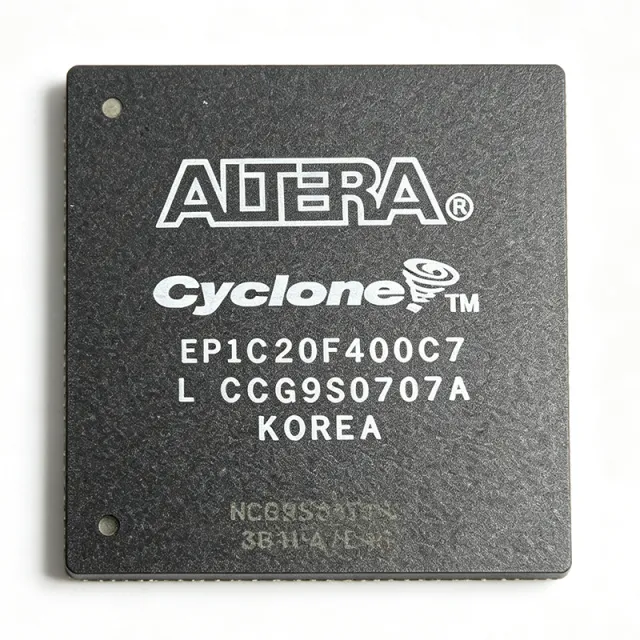
EP1C20F324C6N
EP1C20F324C6N - Cyclone FPGA 20K LE 324-BGA | Intel / Altera
The Intel / Altera EP1C20F324C6N is a low-cost Cyclone® family Field Programmable Gate Array (FPGA) with 20,060 logic elements (LEs), 294,912 bits of embedded RAM, and 233 user I/Os, housed in a 324-ball FineLine BGA (FBGA-324) package measuring 19 mm × 19 mm with 1.0 mm ball pitch. The "C6" speed grade and "N" lead-free suffix indicate a commercial-temperature, lead-free device rated for operation up to approximately 405 MHz internal operation. The Cyclone family targets high-volume, cost-sensitive applications where designers need programmable logic without the power and cost overhead of high-end FPGAs.
A Field-Programmable Gate Array (FPGA) is a semiconductor integrated circuit composed of configurable logic blocks (CLBs), programmable interconnects, and I/O cells that the designer can re-program after manufacture to implement arbitrary digital logic, glue logic, state machines, and parallel datapaths. In the system hierarchy, FPGAs sit alongside microcontrollers and ASICs in the broader class of programmable logic devices (PLDs), and are differentiated by their parallel architecture, ability to handle wide datapaths, and on-chip memory. The Cyclone family was Altera's (now Intel's) entry-level, high-volume FPGA line, fabricated on a 0.13 µm SRAM process, with on-chip multipliers, PLL-based clock management, and support for external memory interfaces including DDR SDRAM and FCRAM.
Key features of the EP1C20F324C6N include 20,060 LEs arranged in 2,006 logic array blocks (LABs), 294,912 bits (approximately 36 Kbit) of M4K embedded memory blocks, up to 233 user I/Os, embedded 18 × 18 multipliers for DSP operations, and up to two PLLs for clock generation and management. The device supports multiple I/O standards including LVTTL, LVCMOS, PCI, SSTL, and LVDS, and is configured via JTAG or Altera's serial configuration devices. The 1.5 V core supply and 1.5 V / 2.5 V / 3.3 V I/O supplies are powered from separate rails, with power consumption strongly dependent on toggle rate and utilization.
From an architectural standpoint, the Cyclone LE contains a 4-input look-up table (LUT), a programmable register, a carry chain for arithmetic, and a cascade chain for wide fan-in logic. The M4K memory blocks can be configured as true dual-port, simple dual-port, or single-port RAM, ROM, or FIFO buffers with parity support. The PLL blocks support clock multiplication, division, phase shifting, and external clock feedback for precise system-level timing alignment.
Typical applications for the EP1C20F324C6N include display controllers and LCD panel drivers, industrial I/O expansion and protocol bridging, low-cost video processing pipelines, glue logic in telecom and networking line cards, motor control and industrial automation, and consumer electronics such as set-top boxes, printers, and digital photo frames. The combination of moderate logic density, embedded multipliers, and on-chip RAM makes it well-suited to mid-complexity control-plane and datapath tasks.
When designing with this part, allocate at least four dedicated power layers or planes (1.5 V core, PLL analog supply, I/O banks, and GND) and follow the Altera Cyclone Hardware Design Guidelines for decoupling, including 100 nF + 10 µF per power pin and a bulk capacitor per supply rail. The 1.0 mm-pitch FBGA-324 requires a 4-6-4 trace escape on a high-layer-count PCB and ENIG or OSP surface finish for reliable BGA assembly.
This page synthesizes distributor pricing, drop-in alternatives from the same Cyclone family, and practical design notes not found in the manufacturer datasheet alone.
Cotação
Contato