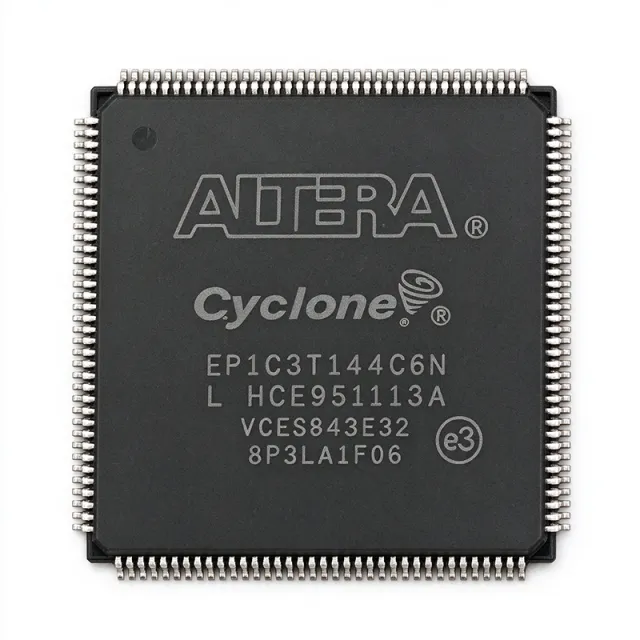
EP1C6Q240C7N
EP1C6Q240C7N - Cyclone FPGA, 5980 LE, QFP-240 | Intel
The Intel EP1C6Q240C7N is a Cyclone field-programmable gate array (FPGA) containing 5,980 logic elements, 92,160 RAM bits, and 185 user I/O pins in a 240-pin BFQFP package. It belongs to the first-generation Cyclone family originally developed by Altera and now supported by Intel. The -7 speed grade and lead-free “N” finish make this component suitable for logic integration applications that require moderate density, flexible I/O, and a surface-mount quad flat pack that is easier to route than a fine-pitch BGA.
A field-programmable gate array is an integrated circuit whose logic fabric can be configured after manufacturing, unlike a fixed-function ASIC or standard logic device. The FPGA is the most flexible member of the programmable logic family, sitting above CPLDs in capacity and below high-end 28 nm and 16 nm FPGAs in complexity. Designers use FPGAs when time-to-market, reconfigurability, or parallel processing requirements outweigh the per-unit cost advantages of a fixed ASIC. In a typical system hierarchy, an FPGA belongs to “Programmable Logic ICs > FPGA > SRAM-based FPGA,” and the EP1C6 is one of the small-to-medium members of that category.
Key verified specifications from distributor and datasheet-index data include 5,980 logic elements, 92,160 RAM bits, and 185 user I/O pins in a 240-BFQFP package. As a Cyclone EP1C6 part, it provides the architectural balance of look-up-table logic, embedded memory, and multiple I/O banks. The -7 speed grade is the mainstream commercial speed option in this family, while the “N” suffix indicates a RoHS-compliant lead-free assembly. The 240-pin PQFP package has a relatively large pitch and wide availability of low-cost testing sockets, making it practical for prototype and low-to-medium volume applications.
Architecturally, the Cyclone EP1C6 uses an SRAM-based configuration fabric and must be loaded from an external configuration device or host at power-up. The device includes dedicated clock networks and multiple I/O banks, though the verified web snippets do not provide exhaustive details about PLL count, core voltage, or special transceivers. The 185 user I/O count allows a wide parallel bus to be brought out to the PCB, which is useful for SDR, motor control, and simple video capture. The 92,160 RAM bits support shallow FIFOs and line buffers, while the 5,980 logic elements implement modest state machines and datapaths.
Typical applications include industrial motor-control interfaces, video image capture and display, communication protocol bridges, and low-cost test-and-measurement controllers. Because this is an older Cyclone family, it is not recommended for new high-performance designs, but it remains relevant for legacy product sustainment, educational projects, and designs already qualified around the 240-pin BFQFP footprint. Designers evaluating it should confirm supply, thermal, and configuration requirements from the official Cyclone device handbook before committing a board.
The main design consideration for EP1C6Q240C7N is that SRAM-based FPGAs require a configuration source and a controlled power-up sequence. Use a compatible serial configuration device or host interface, and verify the core and I/O voltage rails before layout completion. Also remember that Cyclone I FPGAs are near or past end-of-life, so lifetime-buy planning is essential for production systems.
This page synthesizes distributor stock information, cross-reference links, package details, and engineering considerations for the EP1C6Q240C7N that do not appear together in any single datasheet index result.
Cotação
Contato