Produtos (39.000+)

IRS2053MTRPBF 3-Ch 10-15V 6.2W Class D Driver | Infineon
IRS2053MTRPBF

IRS2053MTRPBF 3-Ch 10-15V 6.2W Class D Driver | Infineon

The Infineon IRS2053MTRPBF is a three-channel, high-performance Class D audio amplifier driver with integrated PWM modulators and protection, designed for a 10 V to 15 V supply and a 48-pin MLPQ (7 x 7 mm) package. The verified data identifies it as a 3-channel device associated with 6.2 W output and 60 dB gain, making it suitable for external-MOSFET automotive audio power stages. Its 0.50 mm package pitch supports compact layouts, while its -40 °C to 125 °C operating range addresses harsh automotive environments. The device is RoHS compliant according to the provided source. A Class D audio driver is a controller or gate-drive device that uses pulse-width modulation to drive external power MOSFETs in an audio half-bridge or full-bridge output stage. Unlike a conventional linear audio amplifier, the switching output stage can deliver audio with lower power dissipation than a comparable linear stage, although EMI filtering and careful layout remain important. The IRS2053 integrates three channels so a complete three-channel amplifier can be formed with external MOSFETs and passive components. Key verified features include three audio channels, a 10 V to 15 V supply range, 6.2 W output capability in the cited series description, 60 dB gain, a 48-MLPQ package measuring 7 x 7 mm, and 0.50 mm pitch. The package also has an exposed pad according to the supplied product-page description. The -40 °C to 125 °C temperature range supports automotive and industrial audio systems, while RoHS compliance supports regulated manufacturing and product-environment requirements. The IRS2053 uses floating analog inputs and a protection-control interface intended for external MOSFET half-bridge stages. In implementation, the three PWM outputs drive external power devices, while input conditioning, gate resistors, supply decoupling, output filtering, and protection components complete the power stage. Exact output power, modulation details, pin names, current limits, and timing values were not included in the provided verified data and must be confirmed in the manufacturer datasheet before layout or production use. Typical applications include automotive head units, three-channel infotainment systems, seat or console audio, and compact external Class D power modules. A three-channel arrangement can support front left, front right, and a center, subwoofer, or rear channel, depending on the amplifier architecture. The 10 V to 15 V supply range is suitable for automotive battery-derived rails after suitable regulation and filtering, but the exact automotive transient and operating requirements are not provided here. Designers should follow the manufacturer datasheet for exposed-pad thermal design, input filtering, power-supply decoupling, MOSFET selection, gate-loop layout, EMI control, and protection configuration. Because the provided data does not include complete pin-level definitions or verified electrical limits, no pin-level substitute should be assumed merely because it uses a nominally similar package.

Cotação Contato
IRS2092PBF - 500W Protected Class D Driver | Infineon
IRS2092PBF

IRS2092PBF - 500W Protected Class D Driver | Infineon

The Infineon Technologies IRS2092PBF is a protected, high-voltage, mono Class D audio amplifier driver with an integrated PWM modulator, operating from a 10 V to 18 V supply and supporting a 500 W audio power stage. It is packaged in a 16-lead PDIP package and requires two external MOSFETs plus a few external components to realize a complete protected Class D power amplifier. A Class D audio amplifier driver is a controller for a switching audio power stage. It accepts an analog audio signal, generates the required PWM drive signals, and controls external power transistors that deliver current efficiently to a loudspeaker. Within the power-management and audio hierarchy, the IRS2092 sits between the audio source and discrete output MOSFETs rather than directly driving a speaker. Key features include a high-voltage, high-performance Class D architecture, integrated PWM modulation, floating inputs for straightforward half-bridge implementation, and programmable bidirectional over-current protection. The 16-lead PDIP package supports through-hole assembly. The verified distributor listing identifies the device as a one-channel mono Class D amplifier IC and describes its operating supply as 10 V to 18 V. The device is intended for high-power audio systems where external power MOSFETs provide the speaker current. Its modulator determines the switching command delivered to those devices, while the protection function helps prevent excessive current during abnormal output conditions. The exact output-power conditions, switching frequency, propagation delay, quiescent current, and thermal limits were not supplied in the retrieved data and should be confirmed from the manufacturer datasheet before final design release. Typical uses include mono subwoofer amplifiers, professional audio power stages, high-current speaker drivers, and compact Class D amplifier modules. The architecture is particularly relevant where a bridge-tied half-bridge output is desired and where two external MOSFETs are acceptable. Designers should treat MOSFET selection, gate-loop layout, heat-sink sizing, dead time, output filtering, and protection thresholds as system-level engineering tasks. The driver IC does not eliminate the need for a correctly rated power stage, and its published 500 W capability is not an all-load guarantee. This page combines verified distributor specifications, datasheet links, replacement-screening constraints, and practical implementation guidance. It distinguishes confirmed IRS2092PBF facts from parameters that remain unavailable in the supplied source set.

Cotação Contato
IRS2092SPBF - Protected 100V Class-D Driver | Infineon
IRS2092SPBF

IRS2092SPBF - Protected 100V Class-D Driver | Infineon

The Infineon Technologies IRS2092SPBF is a protected, high-voltage, mono Class-D audio amplifier driver rated for a 100 V maximum supply and 500 ns gate-drive timing, integrated with an 800 kHz PWM modulator and protection functions. It is packaged in a narrow 16-lead SOIC. The device works with two external power MOSFETs and a small number of passive components to implement a complete protected Class-D audio power stage. A Class-D audio amplifier driver is a specialized gate-drive IC that converts an analog audio input into high-frequency PWM signals for external half-bridge MOSFETs. The IRS2092SPBF belongs to the audio-amplifier-driver hierarchy, combining modulator, gate-driver, and protection functions in one controller. Unlike a finished audio output amplifier, it requires external power transistors, gate resistors, passive networks, and an appropriate output filter. The verified product information identifies the device as a mono, analog-input Class-D amplifier with digital audio amplification behavior. Its stated 100 V voltage class, 500 ns timing value, and 800 kHz associated switching specification are useful for evaluating gate-drive bandwidth and system architecture. The integrated protection is intended to improve robustness in external-MOSFET audio power stages, although exact protection thresholds and conditions must be confirmed from the manufacturer datasheet. Typical uses include compact stereo or multichannel audio systems, powered speakers, automotive audio infrastructure, home-theater equipment, and industrial audio products. The device is most appropriate when the designer wants controller-level flexibility with discrete MOSFET selection rather than a fixed integrated power amplifier. The 16-SOIC package also makes it compatible with conventional surface-mount PCB assembly processes. A critical design consideration is that controller ratings do not determine the final speaker power. Output power depends on external MOSFET selection, supply voltage, modulation strategy, output filter, transformer or speaker impedance, and thermal design. Use the manufacturer datasheet and application circuits for gate-drive timing, dead-time behavior, fault handling, bootstrap or high-side supply requirements, and PCB layout. This product record consolidates the verified manufacturer and distributor descriptions with practical application guidance and explicitly identifies parameters that require confirmation before layout or production release.

Cotação Contato
IRS2092STRPBF - 200V Mono Class D Audio Driver | Infineon
IRS2092STRPBF

IRS2092STRPBF - 200V Mono Class D Audio Driver | Infineon

Infineon Technologies IRS2092STRPBF is a high-voltage, high-performance mono Class D audio amplifier driver with an integrated PWM modulator and protection functions. It operates from a 200 V supply according to the Mouser product listing, uses an integrated analog input, and drives external MOSFETs to form a complete audio power stage. The device is packaged in a narrow 16-lead SOIC. Its architecture supports floating inputs for convenient half-bridge implementation, programmable bidirectional over-current protection with self-reset, and programmable preset deadtime. These characteristics position the IRS2092STRPBF as a gate-driver-class audio IC rather than a conventional line-output amplifier: it accepts a low-level audio signal and controls the switching of external power MOSFETs that deliver energy to a loudspeaker. The external MOSFET selection remains central to output power, switching loss, and thermal performance. Use the manufacturer datasheet for the complete electrical limits, truth tables, timing characteristics, protection behavior, pin descriptions, and recommended application circuit. The supplied search results also identify the device as a 16-SOIC, single-channel Class D amplifier driver and describe the IRS2092 family as intended for high-voltage audio systems. In a typical implementation, the IRS2092STRPBF drives a self-oscillating or externally controlled half-bridge stage, while protection logic helps contain overload conditions. Board layout, gate-loop layout, and the high-voltage power stage deserve careful review because the driver interfaces directly with fast-switching external MOSFETs.

Cotação Contato
IRS20954SPBF - Class D Audio Driver, 2-Ch, 16-SOIC | Infineon
IRS20954SPBF

IRS20954SPBF - Class D Audio Driver, 2-Ch, 16-SOIC | Infineon

The Infineon IRS20954SPBF is a 2-channel protected digital audio driver designed for Class D audio amplifier applications, housed in a 16-pin SOIC package with surface-mount mounting. The device combines high-voltage gate-drive capability with integrated analog protection features, targeting single-ended or bridge-tied-load (BTL) Class D output stages in consumer and prosumer audio equipment. The PBF suffix indicates lead-free (Pb-free) terminal finish per RoHS requirements. A Class D audio driver is a specialized gate-driver / controller that translates low-level PWM or analog audio inputs into the high-current, high-voltage switching signals required by the output MOSFETs in a Class D amplifier. The IRS20954 belongs to the audio-special-purpose IC family, sitting hierarchically between a DSP/modulator front-end and a discrete power-MOSFET output stage, and is itself a member of the broader switch-mode power semiconductor driver category. Key features include a floating PWM input that enables easy half-bridge implementation, integrated programmable bi-directional over-current protection with a self-reset function, programmable compensated preset dead-time for improved THD performance, and high noise immunity. The 2-channel architecture supports stereo BTL or single-ended mono output configurations, and the integrated protection block reduces external component count compared to discrete gate-driver + comparator solutions. The IRS20954 uses a high-side/low-side gate-driver topology with internal level shifting, allowing direct interface to a PWM modulator or analog front-end. The bidirectional OC protection monitors load current through the low-side FET R_DS(on) without an external shunt resistor, simplifying layout and reducing conduction loss. Preset dead-time is trimmed at the factory to optimize shoot-through immunity versus THD at the switching node. Typical applications include home theater receivers, powered subwoofers, multimedia speakers, automotive head-unit amplifiers, and pro-sound active loudspeakers. The 16-SOIC footprint is footprint-compatible with the related IRS20955 and IRS20957 family members, allowing PCB reuse across product variants. When designing with this part, observe the absolute maximum ratings on VCC and bootstrap voltages, and follow the application note for output-stage MOSFET selection to ensure OC trip thresholds remain within the safe operating area under all load conditions.

Cotação Contato
IRS20954STRPBF - 2-Channel Protected Audio Driver | Infineon
IRS20954STRPBF

IRS20954STRPBF - 2-Channel Protected Audio Driver | Infineon

The Infineon Technologies IRS20954STRPBF is a 2-channel protected digital audio line driver in a 16-pin SOIC package. It accepts floating PWM inputs for straightforward half-bridge implementation and incorporates programmable, bidirectional over-current protection with a self-reset function. The device also provides programmable compensated preset dead time to improve total harmonic distortion, making it suited to class-D audio output stages and other protected PWM power-stage drivers. A digital audio driver is an interface and protection IC positioned between a PWM controller or digital signal processor and a power-converter stage. Within the signal chain, this category combines logic-level command processing with protection and gate-drive support. The resulting device belongs to the broader power-management IC hierarchy while providing the timing and fault-handling functions needed to operate external half-bridge power switches safely. The principal verified features include two-channel operation, floating PWM inputs, programmable bidirectional over-current protection, automatic self-reset after a protected fault, and compensated preset dead time. Compensation of the preset dead time can reduce distortion introduced when the bridge switches between its output states. The self-reset behavior also allows the driver to recover without requiring an external system reset after the protected condition has cleared. Because the IRS20954STRPBF is a driver rather than the audio output power stage itself, its operation depends on appropriately rated external switching devices. Its protected digital-drive architecture supports the implementation of half-bridge arrangements commonly used in audio amplification. Detailed electrical limits, propagation delays, drive-current capability, thermal ratings, and recommended external components must be confirmed in the manufacturer datasheet before layout or production use. Typical uses include digitally controlled class-D audio amplifiers, speaker-drive power stages, compact consumer-audio systems, and industrial amplification equipment where fault recovery and controlled switching transitions are important. The floating PWM input arrangement can simplify use with systems that drive each channel using complementary or single-ended PWM information. The appropriate external MOSFETs and passive network remain application-specific. The primary design consideration is MOSFET selection. The external devices must satisfy the application voltage, current, switching-loss, and thermal requirements, while their gate characteristics must remain compatible with the driver. PCB layout should minimize gate-loop inductance and keep switching-node copper compact. Protection settings, dead-time programming, and fault-response behavior must also be checked against the intended speaker impedance and amplifier architecture. This page consolidates verified distributor availability, exact catalog identifiers, the documented feature set, and engineering-focused application guidance. It distinguishes confirmed data from parameters that still require the official datasheet, providing a useful starting point for sourcing and design review without assigning unsupported electrical values.

Cotação Contato
IRS20955STRPBF - 2-Channel Audio Line Driver | Infineon
IRS20955STRPBF

IRS20955STRPBF - 2-Channel Audio Line Driver | Infineon

Infineon Technologies IRS20955STRPBF is a two-channel audio line driver and peripheral driver IC designed for Class D audio power-amplifier applications. The device supports a supply voltage described as 12 V in the verified technical listing, operates from -40 C to +125 C, and is packaged in a 16-pin SOIC-16 package using the MS-012AC outline. Its verified feature set includes a floating PWM input for straightforward half-bridge implementation, programmable bidirectional over-current protection with self-reset, and programmable preset behavior. The IRS20955 family is identified as a 120 W x 2-channel Class D audio power-amplifier driver, while an alternative manufacturer listing describes the IRS20955STRPBF as a 100 V, 1.2 A, two-output high-side/low-side half-bridge driver. The device is therefore positioned between low-power control logic and the output stage of a robust audio amplifier. Its 16-pin surface-mount construction supports compact audio products while retaining the thermal and assembly characteristics expected of an SOIC package. Infineon’s IRS20955 family also appears in the verified cross-reference data as closely related to IRS20953, IRS20956, and IRS20957, with application-dependent distinctions. Because exact pin-level compatibility, electrical limits, pricing, and some package details were not supplied for every candidate or parameter in the retrieved data, those items are marked for engineering verification rather than inferred. This page combines verified distributor descriptions, datasheet references, and practical design guidance for engineers evaluating IRS20955STRPBF in audio amplifier designs.

Cotação Contato
IRS20965STRPBF - 500W Mono Class D Driver | Infineon
IRS20965STRPBF

IRS20965STRPBF - 500W Mono Class D Driver | Infineon

The Infineon Technologies IRS20965STRPBF is a high-voltage, high-speed MOSFET driver for mono Class D audio amplifier applications, rated by the manufacturer for operation up to 500 W output power in a 16-pin SOIC package. The device provides high-side and low-side floating PWM inputs, programmable bidirectional over-current detection with self-reset, an over-current sensing output, and shoot-through prevention logic. Its operating supply range is listed as 10 V to 15 V, and its high-voltage and high-speed architecture positions it for demanding audio power-stage designs. A Class D audio driver is a gate-drive controller used between a PWM command signal and the power MOSFETs of an audio output stage. The IRS20965STRPBF belongs to the MOSFET-driver hierarchy, where a MOSFET driver controls power transistors rather than directly delivering audio output to a speaker. By supporting independently floating high-side and low-side PWM inputs, the driver can operate the two output transistors from a single low-voltage control domain while the power stage switches a substantially higher bus voltage. The verified manufacturer features include bidirectional over-current protection, self-reset behavior, a dedicated over-current sensing output, and shoot-through prevention. These functions are particularly relevant to speaker systems in which abnormal DC, load mismatch, or transistor faults can increase power-device stress. Bidirectional current sensing also allows detection conditions to be evaluated in both switching directions, while the self-reset function can return the protection circuit toward its normal operating state after the monitored fault condition is removed. The device is a 16-pin SOIC and supports high-side and low-side floating PWM inputs. This integration allows a compact Class D amplifier controller to be placed near the output MOSFETs while separating the high-voltage switching environment from the low-voltage command circuitry. Independent floating inputs can also support timing adjustments, but board-level propagation delays and mismatched gate-drive paths should be reviewed before a design is released for production. Typical uses include mono Class D speaker amplifiers, high-power consumer-audio systems, professional audio output stages, and industrial audio systems operating from a high-voltage bus. The 10 V to 15 V supply range and 500 W capability make the part most relevant where a compact controller is preferred over discrete high-voltage gate-drive circuitry. Infineon presents it as an audio-amplifier driver rather than a complete power amplifier, so external output MOSFETs, passive protection networks, gate resistors, and a suitable output filter remain required. For robust implementation, use low-inductance gate-drive layouts, keep the high-voltage switching loop compact, and place current-sense and protection components where their sensing relationships are clear. The verified sources do not provide the complete pin mapping, timing limits, thermal ratings, or detailed application-circuit values, so those items must be confirmed in the manufacturer datasheet before layout release. This page distinguishes documented facts from parameters that still require datasheet verification while adding practical selection and implementation guidance.

Cotação Contato
IRS2461SXUMA1 - 1-Channel Class-D Audio Amp | Infineon
IRS2461SXUMA1

IRS2461SXUMA1 - 1-Channel Class-D Audio Amp | Infineon

The Infineon Technologies IRS2461SXUMA1 is a discrete 1-channel Class-D audio amplifier IC with an analog audio input and a 20-lead SOIC package. The verified manufacturer listing identifies the IRS2461S family as a discrete Class-D audio amplifier, while the distributor results classify IRS2461SXUMA1 as an audio amplifier IC. Its defined role is to drive a single speaker channel from an analog source, making it relevant to compact consumer audio, portable speakers, soundbars, and other single-channel amplification systems. A Class-D audio amplifier is a switching power amplifier that uses transistor switching stages to deliver audio energy to a speaker. Compared with a linear audio amplifier, the Class-D category is associated with high conversion efficiency, but the verified data supplied for IRS2461SXUMA1 does not state output power, efficiency, switching frequency, THD+N, load impedance, or thermal limits. Those parameters must therefore be confirmed in the manufacturer datasheet before sizing a speaker, selecting a heatsink, or setting gain. The verified package information is specific: Infineon lists the IRS2461S family in a 20-lead SOIC package. The 20-lead package is suitable for conventional surface-mount PCB assembly, while the exact exposed-pad arrangement and pin functions are not present in the supplied data. The LCSC result reports availability from $2.4487, and Heisener reports a reference unit price of $3.4419 with 7,536 pieces in stock; these commercial figures are retained as separate source observations and are not treated as a universal price quote. Typical design use places the analog audio input at the amplifier, with speaker-drive connections and bypass or support networks selected according to the manufacturer reference design. The exact input sensitivity, gain settings, filter values, supply limits, and pin mapping are unavailable in the provided sources. Engineers should use the official Infineon IRS2461S documentation and validate acoustic output, distortion, thermal behavior, and EMI performance in the final enclosure. This page emphasizes verified sourcing information and clearly identifies missing technical fields rather than estimating them. It combines the manufacturer product classification, distributor observations, package information, application context, and engineering caveats for engineers evaluating an audio amplifier IC.

Cotação Contato
IS43QR16512B-062AABL - 8Gb DDR4 SDRAM 512Mx16 | ISSI
IS43QR16512B-062AABL

IS43QR16512B-062AABL - 8Gb DDR4 SDRAM 512Mx16 | ISSI

The IS43QR16512B-062AABL is an 8Gb DDR4 SDRAM organized as 512Mx16, operating from a 1.2V supply. It supports data transfer rates up to 3200 MT/s with a CAS latency of 22-22-22, and is housed in a 96-ball TWBGA package (7.5mm x 13.5mm). This memory IC is designed for high-performance computing, networking, and industrial applications requiring high bandwidth and low power consumption. DDR4 SDRAM (Double Data Rate 4 Synchronous Dynamic Random-Access Memory) is a type of volatile memory that transfers data on both edges of the clock signal, doubling the data rate compared to DDR3. It uses an 8n prefetch architecture, enabling high-speed data transfer while maintaining lower power consumption through a reduced supply voltage of 1.2V. DDR4 is the industry standard for main memory in servers, desktops, and embedded systems, offering improved speed, density, and reliability over previous generations. Key features include a 1.2V power supply, 3200 MT/s data rate, 19ns tRCD (RAS-to-CAS delay), and a 96-ball TWBGA package. The device supports on-die termination (ODT), programmable read/write latencies, and auto-refresh and self-refresh modes. It is RoHS compliant and operates over a temperature range of 0°C to +95°C (case temperature). The IS43QR16512B uses a high-speed CMOS process and an 8n prefetch architecture, which allows two data words to be transferred per clock cycle at the I/O pins. This design achieves high bandwidth while minimizing power consumption. The device includes a mode register for programming various operating modes, including burst length, CAS latency, and test modes. It also supports error correction code (ECC) for enhanced data integrity in critical applications. Typical applications include high-performance servers, networking equipment (routers, switches), data centers, and industrial computing systems. The high density and speed make it suitable for memory-intensive tasks such as virtualization, real-time analytics, and high-frequency trading. Its low power consumption is beneficial for power-constrained embedded systems. When designing with this DDR4 SDRAM, ensure proper signal integrity by maintaining controlled impedance traces and using appropriate termination. The device requires a stable 1.2V supply and a separate VTT termination voltage. Follow the manufacturer's layout guidelines for the 96-ball TWBGA package to minimize crosstalk and ensure reliable operation at 3200 MT/s.

Cotação Contato
IS43TR16256A-125KBL - 4Gb DDR3 SDRAM 256Mx16 | ISSI
IS43TR16256A-125KBL

IS43TR16256A-125KBL - 4Gb DDR3 SDRAM 256Mx16 | ISSI

The IS43TR16256A-125KBL is a 4Gbit DDR3 SDRAM organized as 256M x 16, manufactured by Integrated Silicon Solution Inc (ISSI). It operates at a standard voltage of 1.5V (VDD and VDDQ) with a data rate of 1600MT/s (800 MHz clock), and is available in a 96-ball TWBGA (9x13mm) package. This memory IC is designed for high-speed data transfer in computing, networking, and industrial applications. DDR3 SDRAM (Double Data Rate Type 3 Synchronous Dynamic Random-Access Memory) is a type of volatile memory that transfers data on both edges of the clock signal, effectively doubling the data rate compared to DDR2. It is a key component in systems requiring high bandwidth and low latency, such as servers, routers, and embedded processors. DDR3 operates at lower voltages (1.5V or 1.35V for DDR3L) than previous generations, reducing power consumption. Key features include a 4Gbit density, 16-bit I/O width, 800 MHz clock frequency, and a CAS latency of 11 (CL=11) at 1600MT/s. The device supports on-die termination (ODT), programmable CAS latency, and burst lengths of 8 and 4 (with burst chop). It also features auto refresh and self refresh modes for power saving. The 96-ball TWBGA package provides a compact footprint suitable for space-constrained designs. The IS43TR16256A-125KBL uses a high-performance CMOS process and includes a DLL (Delay-Locked Loop) for precise timing alignment. It supports a burst length of 8 with a burst chop of 4, and features programmable read and write latencies. The device also includes a temperature-compensated self-refresh (TCSR) mode to reduce power consumption at high temperatures. Typical applications include main memory for embedded systems, networking equipment (routers, switches), industrial PCs, and high-performance computing modules. Its 1.5V operation and 1600MT/s speed make it suitable for a wide range of DDR3-based designs. When designing with this device, ensure proper decoupling capacitors near the VDD and VDDQ pins, and follow the PCB layout guidelines for DDR3 routing to maintain signal integrity. The device requires a 1.5V supply and a separate VDDQ supply, both with tight tolerance (±0.075V).

USD $19,09 Contato
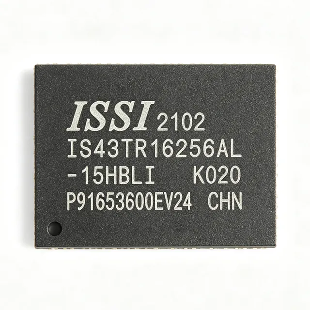
IS43TR16256A-15HBL-TR - 4Gb DDR3 SDRAM 667MHz | ISSI
IS43TR16256A-15HBL-TR

IS43TR16256A-15HBL-TR - 4Gb DDR3 SDRAM 667MHz | ISSI

The IS43TR16256A-15HBL-TR is a 4Gbit DDR3 SDRAM organized as 256M x 16, operating at a clock frequency of 667 MHz (data rate 1333 Mbps) with a CAS latency of 20 ns. It is housed in a 96-ball TWBGA (9x13 mm) package and operates from a 1.5V power supply. This memory IC is designed for high-bandwidth applications requiring reliable, high-speed data storage and retrieval. DDR3 SDRAM (Double Data Rate Type 3 Synchronous Dynamic Random-Access Memory) is a type of synchronous dynamic random-access memory with a high bandwidth interface, double the data rate of DDR2. It achieves higher transfer rates by transferring data on both edges of the clock signal, effectively doubling the data rate without increasing the clock frequency. DDR3 is part of the SDRAM family, which includes DDR, DDR2, DDR4, and DDR5, and is widely used in computing, networking, and embedded systems. Key features include a 4Gbit density, 16-bit I/O organization, 667 MHz clock speed, and a 20 ns CAS latency. The device supports programmable CAS latency, burst lengths of 8 and 4 (with burst chop), and on-die termination (ODT) for improved signal integrity. It also features auto-refresh and self-refresh modes for power saving, and a temperature-compensated self-refresh (TCSR) option. The IS43TR16256A-15HBL-TR utilizes a high-performance CMOS process and a bank architecture with 8 internal banks, enabling efficient interleaving and high throughput. The device includes DLL (Delay-Locked Loop) for precise timing alignment and supports write leveling and read leveling for system timing calibration. Its low power consumption and high speed make it suitable for a wide range of applications. Typical applications include networking equipment (routers, switches), industrial computing, embedded systems, and consumer electronics such as set-top boxes and smart TVs. The 1.5V operation and 96-ball TWBGA package allow for compact PCB designs with good thermal performance. When designing with this device, ensure proper decoupling capacitors near the power pins and follow the layout guidelines in the datasheet to minimize signal integrity issues. The device requires a stable 1.5V supply and a reference voltage (VREF) for the I/O.

USD $10,34 Contato
IS43TR16256AL-107MBL - 4Gb DDR3L SDRAM 256Mx16 | ISSI
IS43TR16256AL-107MBL

IS43TR16256AL-107MBL - 4Gb DDR3L SDRAM 256Mx16 | ISSI

The IS43TR16256AL-107MBL is a 4Gb DDR3L SDRAM organized as 256Mx16, operating at 1.35V with a data rate of 1866MT/s. It is housed in a 96-ball TWBGA (9x13mm) package, offering high density and low power consumption for a wide range of computing and embedded applications. DDR3L (Low Voltage DDR3) is a type of synchronous dynamic random-access memory that operates at 1.35V, reducing power consumption by about 15% compared to standard 1.5V DDR3. It is part of the DDR3 SDRAM family, which uses double data rate architecture to transfer data on both edges of the clock, achieving high bandwidth. DDR3L is commonly used in mobile devices, networking equipment, and industrial computing where power efficiency is critical. Key features include a parallel interface with 933 MHz clock speed, 20 ns access time, and support for 1866MT/s data rate. The device supports various burst lengths (8 and 4 with burst chop), on-die termination (ODT), and programmable CAS latency. It operates over a temperature range of 0°C to +95°C (case) and is RoHS compliant. The IS43TR16256AL-107MBL utilizes advanced DRAM process technology, providing high reliability and performance. It features auto-refresh and self-refresh modes, which are essential for low-power standby operation. The 96-ball TWBGA package ensures excellent thermal and electrical performance, making it suitable for space-constrained designs. Typical applications include networking routers and switches, enterprise storage systems, industrial PCs, and embedded computing platforms. Its low voltage and high density make it ideal for memory-intensive applications where power efficiency is a priority. When designing with this device, ensure proper decoupling capacitors are placed near the power pins to minimize noise. The DDR3L interface requires careful PCB layout to maintain signal integrity at high speeds, including matched trace lengths and controlled impedance.

Cotação Contato
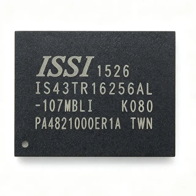
IS43TR16256AL-107MBLI - 4Gb DDR3L SDRAM 256Mx16 | ISSI
IS43TR16256AL-107MBLI

IS43TR16256AL-107MBLI - 4Gb DDR3L SDRAM 256Mx16 | ISSI

The IS43TR16256AL-107MBLI is a 4Gb DDR3L SDRAM organized as 256M x 16 bits, operating at a clock speed of 933 MHz (data rate 1866 Mbps) with a supply voltage of 1.35V. It is housed in a 96-ball TWBGA (9x13mm) package, making it suitable for high-density memory applications in computing, networking, and industrial systems. DDR3L SDRAM (Double Data Rate 3 Low Voltage) is a type of synchronous dynamic random-access memory that operates at a lower voltage (1.35V) compared to standard DDR3 (1.5V), reducing power consumption by up to 20% while maintaining backward compatibility with 1.5V operation. It is part of the DDR3 memory family, which uses double data rate signaling to transfer data on both edges of the clock, achieving high bandwidth for demanding applications. Key features include a 16-bit I/O interface, 4Gbit density, 20ns access time, and support for 1.35V operation with backward compatibility to 1.5V. The device offers high-speed data transfer rates, low power consumption, and is RoHS compliant. The 96-ball TWBGA package provides a compact footprint suitable for space-constrained designs. Technically, the IS43TR16256AL-107MBLI utilizes a 4-bank architecture with 8 internal banks, supporting burst lengths of 8 and 4, and features on-die termination (ODT) for improved signal integrity. It includes programmable CAS latency, additive latency, and write latency, allowing system designers to optimize timing for their specific memory controller. The device also supports auto-refresh and self-refresh modes for power saving. Typical applications include servers, networking equipment, industrial PCs, and embedded systems where high memory density and low power are critical. The 1.35V operation makes it ideal for power-sensitive designs, while the 1866 Mbps data rate supports high-bandwidth workloads. When designing with this device, ensure proper decoupling capacitors near the power pins and follow the layout guidelines in the datasheet to minimize signal integrity issues. The device requires a stable 1.35V supply and careful attention to termination for the address/control and data lines.

Cotação Contato
IS43TR16256AL-107MBLI-TR - 4Gb DDR3L SDRAM 256Mx16 | ISSI
IS43TR16256AL-107MBLI-TR

IS43TR16256AL-107MBLI-TR - 4Gb DDR3L SDRAM 256Mx16 | ISSI

The IS43TR16256AL-107MBLI-TR is a 4Gb DDR3L SDRAM organized as 256Mx16, operating at 1.35V with a data rate of 1866 Mbps (933 MHz clock). It is housed in a 96-ball TWBGA (9x13mm) package and is designed for low-power applications requiring high memory density. This device is backward compatible with 1.5V DDR3, allowing flexible system design. DDR3L SDRAM is a type of double data rate synchronous dynamic random-access memory that operates at a lower voltage (1.35V) compared to standard DDR3 (1.5V), reducing power consumption by about 20%. It is part of the memory hierarchy in computing systems, serving as main memory for processors, and is widely used in servers, networking equipment, and embedded systems where power efficiency is critical. Key features include a parallel interface with 16-bit data bus, 20ns access time, and support for on-die termination (ODT) and DLL-off mode for power saving. The device supports burst lengths of 8 and 4, and includes programmable CAS latency and additive latency. It operates over a temperature range of 0°C to +95°C (case temperature) for standard operation. The IS43TR16256AL-107MBLI-TR utilizes advanced DRAM process technology to achieve high density and low power. It features auto-refresh and self-refresh modes, with a typical self-refresh current of [DATA_NEEDED: self-refresh current]. The device includes a mode register set (MRS) for configuration, and supports write leveling and read leveling for signal integrity in high-speed systems. Typical applications include servers, networking equipment, industrial computing, and embedded systems where high memory density and low power are required. The 1.35V operation makes it ideal for battery-powered devices and energy-efficient data centers. When designing with this device, ensure proper decoupling capacitors near the power pins and follow the PCB layout guidelines in the datasheet to maintain signal integrity at 1866 Mbps. The device requires a stable 1.35V supply and a separate VDDQ supply for the I/O.

USD $5,60 Contato
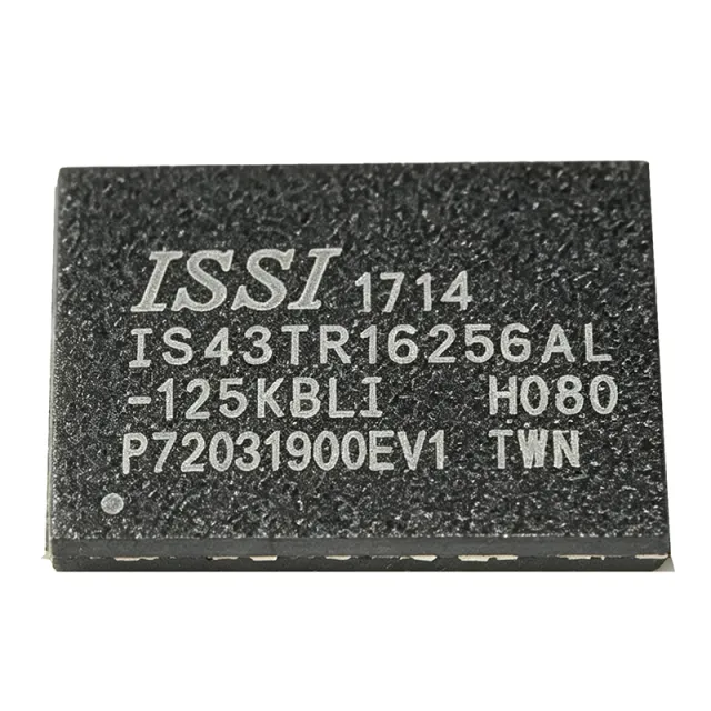
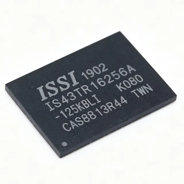
IS43TR16256AL-125KBL - 4Gb DDR3L SDRAM 256Mx16 | ISSI
IS43TR16256AL-125KBL

IS43TR16256AL-125KBL - 4Gb DDR3L SDRAM 256Mx16 | ISSI

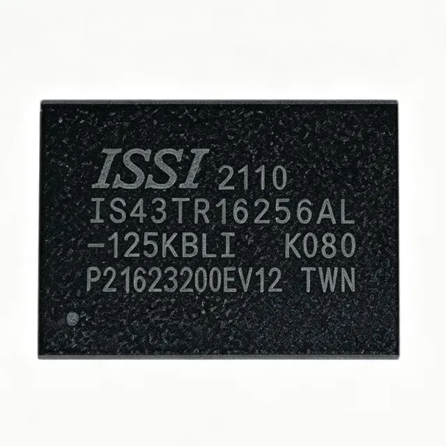
The IS43TR16256AL-125KBL is a 4Gbit DDR3L SDRAM organized as 256M x 16, operating from a 1.35V supply with backward compatibility to 1.5V. It is housed in a 96-ball TWBGA (9x13mm) package and supports data rates up to 1600Mbps (800 MHz clock). This memory IC is designed for high-performance computing, networking, and embedded systems requiring low power and high bandwidth. DDR3L (Double Data Rate 3 Low Voltage) is a type of synchronous dynamic random-access memory (SDRAM) that operates at a lower voltage (1.35V) compared to standard DDR3 (1.5V), reducing power consumption by about 20-30% while maintaining similar performance. It is part of the DDR3 family, which uses double data rate signaling to transfer data on both edges of the clock, and is widely used in laptops, servers, and industrial applications where energy efficiency is critical. Key features include a parallel interface with 16-bit data bus, 800 MHz clock frequency, 20 ns access time, and support for 1.35V operation. The device is RoHS compliant and lead-free, making it suitable for environmentally conscious designs. The 96-TWBGA package offers a compact footprint with a 9x13mm body, ideal for space-constrained PCB layouts. Technically, the IS43TR16256AL-125KBL uses a high-density DRAM process, achieving 4Gbit capacity in a single package. It supports standard DDR3L features such as on-die termination (ODT), programmable CAS latency, and burst lengths of 8. The low voltage operation reduces I/O power, while the 20ns access time ensures fast random access for demanding applications. Typical applications include embedded computing, networking equipment (routers, switches), industrial automation, and automotive infotainment systems. Its low power and high density make it ideal for memory-intensive tasks in portable and battery-powered devices. When designing with this component, ensure proper decoupling capacitors near the power pins and follow the layout guidelines in the datasheet to minimize signal integrity issues at high speeds. The 1.35V supply must be regulated accurately to maintain reliable operation.

Cotação Contato
IS43TR16256AL-125KBLI-TR - 4Gbit DDR3L SDRAM 256Mx16 | ISSI
IS43TR16256AL-125KBLI-TR

IS43TR16256AL-125KBLI-TR - 4Gbit DDR3L SDRAM 256Mx16 | ISSI

The IS43TR16256AL-125KBLI-TR is a 4Gbit DDR3L SDRAM organized as 256M x 16, operating at a clock frequency of 800 MHz (data rate 1600 Mbps) with a CAS latency of 11. It is supplied in a 96-ball TWBGA (9x13 mm) package and is designed for low-voltage operation at VDD and VDDQ = 1.35V, with backward compatibility to 1.5V. This memory IC is part of ISSI's DDR3L family, offering high density and bandwidth for a wide range of applications. DDR3L (Double Data Rate 3 Low Voltage) SDRAM is a type of synchronous dynamic random-access memory that transfers data on both edges of the clock signal, effectively doubling the data rate. The 'L' designation indicates low-voltage operation at 1.35V, reducing power consumption by about 20% compared to standard DDR3 at 1.5V. DDR3L is widely used in mobile devices, embedded systems, and industrial computing where power efficiency is critical. It is backward compatible with 1.5V DDR3, allowing flexible system design. Key features include a 4Gbit density, 16-bit data bus, 800 MHz clock speed, and a burst length of 8. The device supports on-die termination (ODT), programmable CAS latency, and auto-refresh and self-refresh modes. It operates over a temperature range of -40°C to +95°C (TC), making it suitable for industrial environments. The 96-ball TWBGA package provides a compact footprint with excellent thermal and electrical performance. Technically, the IS43TR16256AL-125KBLI-TR uses a 1.35V power supply for both core and I/O, reducing power dissipation. It features a 20ns row cycle time (tRC) and a 20ns row active time (tRAS). The device supports a data transfer rate of 1600 Mbps per pin, delivering high bandwidth for memory-intensive applications. The low-voltage operation and industrial temperature range make it ideal for embedded systems that require reliable performance in harsh conditions. Typical applications include industrial automation, networking equipment, embedded computing, and automotive infotainment systems. The 4Gbit density and x16 organization are well-suited for applications requiring moderate memory capacity with a wide data bus. The low-voltage operation helps extend battery life in portable devices and reduces thermal load in dense systems. When designing with this component, ensure proper decoupling capacitors are placed near the power pins to minimize noise. The DDR3L interface requires careful PCB layout to maintain signal integrity at 1600 Mbps. Refer to the ISSI datasheet for detailed timing parameters and layout guidelines.

USD $8,25 Contato
IS46TR16256A-125KBLA2 - 4Gb DDR3 SDRAM 256Mx16 | ISSI
IS46TR16256A-125KBLA2

IS46TR16256A-125KBLA2 - 4Gb DDR3 SDRAM 256Mx16 | ISSI

The IS46TR16256A-125KBLA2 is a 4Gb DDR3 SDRAM organized as 256Mx16, operating at 1.5V with a data rate of 1600MT/s (800 MHz clock). It is housed in a 96-ball TWBGA (9x13mm) package, offering high-density memory for computing, networking, and industrial applications. This device supports 8 internal banks for concurrent operation and features programmable CAS latency, burst length, and on-die termination (ODT) for signal integrity. DDR3 SDRAM (Double Data Rate Type 3 Synchronous Dynamic Random-Access Memory) is a type of synchronous dynamic random-access memory with a high bandwidth interface, transferring data on both rising and falling edges of the clock. It is the successor to DDR2 and offers higher speeds and lower power consumption, making it a standard choice for main memory in computers, servers, and embedded systems. DDR3 operates at 1.5V, reducing power compared to DDR2's 1.8V, and supports data rates from 800 to 2133 MT/s. Key features include a 20ns tRCD (RAS-to-CAS delay), 290mA operating current, and a temperature range of 0°C to +95°C (Tc). The device is RoHS compliant and supports both standard and low-voltage (1.35V) operation, providing flexibility in power-sensitive designs. The 96-ball TWBGA package with a 9x13mm footprint enables compact PCB layouts, and the 256Mx16 organization simplifies bus design by reducing the number of devices needed for wide data paths. Architecturally, the IS46TR16256A-125KBLA2 uses an 8-bank design with a 16-bit I/O interface, achieving a peak bandwidth of 12.8 GB/s per device. It incorporates DLL (Delay-Locked Loop) for precise clock alignment, and supports programmable read and write latencies. The device also features auto-refresh and self-refresh modes for power management, and on-die termination (ODT) to improve signal quality on high-speed buses. Typical applications include main memory for embedded processors, networking equipment (routers, switches), industrial PCs, and high-performance computing modules. Its high density and speed make it suitable for applications requiring large memory footprints, such as video processing, data acquisition, and telecommunications infrastructure. When designing with this DDR3 device, ensure proper termination and layout for high-speed signals, and follow the JEDEC DDR3 guidelines for power supply decoupling and signal integrity. The device requires a 1.5V supply for VDD and VDDQ, and a separate VREF for address/command signals.

USD $7,20 Contato
IS61C6416AL-12TLI - 1Mb 64Kx16 12ns Async SRAM | ISSI
IS61C6416AL-12TLI

IS61C6416AL-12TLI - 1Mb 64Kx16 12ns Async SRAM | ISSI

The Integrated Silicon Solution Inc (ISSI) IS61C6416AL-12TLI is a 1 Mbit high-speed asynchronous CMOS Static RAM organized as 65,536 words by 16 bits, with 12 ns access time, housed in a 44-pin TSOP Type II industrial-grade package. It operates from a single 4.5 V to 5.5 V supply and provides a 16-bit parallel I/O bus, making it well suited as cache, buffer, or scratchpad memory in 16-bit and 32-bit embedded systems. What is an asynchronous SRAM? An asynchronous SRAM (Static Random-Access Memory) is a volatile memory device whose read and write cycles are triggered directly by address and control-line transitions, with no external clock required. It sits in the computer-memory hierarchy above DRAM in speed and below on-chip cache in density, and is commonly chosen when deterministic, low-latency random access (single-digit to a few tens of nanoseconds) matters more than density or cost-per-bit. Within ISSI's portfolio it belongs to the IS61C6416AL family of 64Kx16 high-speed CMOS SRAMs. Key features of the IS61C6416AL-12TLI include 12 ns typical access time, low-power CMOS operation with CMOS- and TTL-compatible I/O, automatic power-down when deselected, and separate upper-byte (UB) and lower-byte (LB) enables for byte-wide writes. The 44-pin TSOP-II footprint is JEDEC-standard, simplifying PCB layout and second-sourcing. The industrial temperature grade (-40C to +85C) supports harsh-environment deployment. The device is fabricated using ISSI's high-performance CMOS process, yielding an access time of 12 ns while keeping active and standby currents low. Data is retained as long as power is applied, with no refresh cycles. The active-low write enable (WE#) and chip-enable (CE#) signals give the designer full read/write control, and the byte-control pins (UB#, LB#) allow efficient use of the 16-bit data bus in mixed-width systems. Typical applications include networking line cards, industrial control and instrumentation, automotive infotainment subsystems, telecom routers and switches, RAID controllers, set-top boxes, and any 16-bit or 32-bit embedded CPU system that needs a fast external memory for buffers, FIFOs, or lookup tables. The TSOP-II package and standard JEDEC pinout also make it a popular choice for legacy designs that must be maintained or refreshed. When designing with this part, observe the standard SRAM power-supply decoupling practice: place a 0.1 uF ceramic bypass capacitor as close as possible to the VCC and VSS pins. Unused inputs (UB#, LB#, WE#) should be tied to VCC through a pull-up to prevent unwanted writes. Designers should also note that the asynchronous interface means there is no clock-domain crossing required when interfacing to legacy microcontrollers or DSPs that lack an external memory controller with SRAM timing support. This page synthesizes distributor pricing, parametric drop-in alternatives, and practical design notes that are not gathered in the manufacturer datasheet alone, giving engineers a single source for sourcing, replacement, and PCB-layout decisions.

Cotação Contato
IS61WV102416DBLL-10TLI - 16Mb Async SRAM 1Mx16 10ns | ISSI
IS61WV102416DBLL-10TLI

IS61WV102416DBLL-10TLI - 16Mb Async SRAM 1Mx16 10ns | ISSI

The ISSI IS61WV102416DBLL-10TLI is a 16-Mbit high-speed asynchronous CMOS static RAM organized as 1M words by 16 bits, housed in a 48-pin TSOP-I package. According to the ISSI datasheet for the IS61/64WV102416DALL/BLL family, the device operates from a single 2.4V to 3.6V supply (with 3.3V nominal) and provides a 10 ns access time, making it suitable for high-performance memory subsystems where deterministic, low-latency read/write cycles are required without the complexity of a DRAM controller. The 'D' prefix designates the lower-voltage 2.4V-3.6V variant, while the 'BLL' suffix indicates the specific speed grade and package option. Asynchronous static RAM (SRAM) is a volatile memory technology that retains data as long as power is applied, without the refresh cycles required by DRAM. Within the broader memory hierarchy, SRAM sits closest to the processor because of its sub-15 ns access times; it is used for cache, look-up tables, scratch-pad buffers, and FIFO storage in networking, industrial, and embedded systems. Compared with synchronous SRAM (such as QDR or DDR SRAM), asynchronous SRAM uses simple chip-enable, output-enable, and write-enable control signals and is ideal for glue-less processor bus interfaces. The IS61WV102416DBLL-10TLI provides fully static operation (no clock required), TTL-compatible I/O levels, common data-in/data-out bus architecture, and an active-low output enable for bus sharing. Power consumption is minimized through a Chip Enable power-down mode, and the device supports industrial temperature range operation. The CMOS fabrication process delivers high noise immunity and low standby current, both of which are critical for battery-backed or energy-conscious designs. Typical applications include industrial controllers, networking line cards, routers and switches requiring fast look-up tables, automotive telematics (non-safety-critical subsystems), medical instrumentation buffers, RAID controllers, and any embedded CPU/MCU design that needs a large, low-latency external data store beyond the on-chip SRAM budget. The wide word width (x16) is well matched to 16-bit and 32-bit microcontrollers and DSPs. When designing with this device, keep in mind that asynchronous SRAM bandwidth is limited by the controller's ability to issue back-to-back read or write strobes, so the 10 ns access time implies roughly 100 MHz equivalent single-transfer throughput per cycle. Decoupling and signal routing must be handled carefully on long busloads to maximize margin. This page synthesizes distributor pricing, drop-in alternative cross-references, and practical design notes that go beyond the manufacturer datasheet to help engineers evaluate and qualify the part quickly.

Cotação Contato
IS82C54Z96 - 8MHz CMOS Programmable Interval Timer | Renesas
IS82C54Z96

IS82C54Z96 - 8MHz CMOS Programmable Interval Timer | Renesas

The Renesas IS82C54Z96 is a CMOS Programmable Interval Timer manufactured using an advanced 2 micron CMOS process, supplied in a 28-pin PLCC package. It supports clock input frequencies up to 8 MHz and operates from a 4.5 V to 5.5 V single supply. According to the Renesas 82C54 datasheet, the device integrates three independently programmable and functional 16-bit counters, each capable of binary or BCD counting and of handling clock inputs up to 8 MHz (82C54), 10 MHz (82C54-10), or 12 MHz (82C54-12). A programmable interval timer (PIT) is a counter IC that generates precise time delays, event counting, and frequency-division functions under software control. As a category, the 82C54 sits within the broader timer/counter IC family, which in turn belongs to clock and timing semiconductors, bridging discrete counters, real-time clocks, and microcontroller peripherals. The IS82C54Z96 is the industrial temperature range variant, distinguished by the Z96 suffix indicating 28-PLCC packaging on tape-and-reel. Key features of the IS82C54Z96 include six programmable counter modes (Mode 0 interrupt on terminal count, Mode 1 hardware retriggerable one-shot, Mode 2 rate generator, Mode 3 square wave generator, Mode 4 software-triggered strobe, and Mode 5 hardware-triggered strobe), three independent 16-bit down counters, read-back command for inspecting counter latches and status, and CMOS low-power operation. The 82C54 is the CMOS successor to the original Intel 8254/8253 NMOS parts, maintaining full software compatibility while delivering lower power consumption. Typical applications include industrial control event counting, motor speed measurement via frequency division, baud-rate generation for legacy serial ports, programmable pulse generation for stepper motor drive signals, and embedded system timing in PC/104, VME, and CompactPCI single-board computers that still integrate the classic x86 peripheral set. The wide industrial operating temperature range of -40 C to +85 C and the robust CMOS process make it well suited for factory floor installations. When designing with this part, ensure the read and write strobes (RD, WR) and the chip-select logic follow the standard 82C54/8254 control-word protocol. Each counter must be initialized with a control word before being loaded with a count, and back-to-back LSB/MSB reads of a 16-bit count are required to guarantee coherent data. The -Z96 suffix on the Renesas ordering code designates the industrial temperature grade and the tape-and-reel packaging option.

Cotação Contato
ISD17120SY - 120sec Voice Record/Playback IC | Nuvoton | SOIC-28
ISD17120SY

ISD17120SY - 120sec Voice Record/Playback IC | Nuvoton | SOIC-28

The Nuvoton ISD17120SY is a single-chip multi-message voice record and playback IC from the ChipCorder ISD1700 family, providing 80 to 240 seconds of audio storage (120 seconds typical) in a 28-pin SOIC package. It operates from a single 2.4 V to 5.5 V supply and supports both pushbutton and SPI control interfaces, enabling flexible user interaction in standalone or microcontroller-driven systems. A voice record/playback IC is a fully integrated solid-state audio recorder that combines non-volatile memory, an analog microphone preamplifier, anti-aliasing filter, automatic gain control (AGC), speaker driver, and a PWM output stage on a single die. It belongs to the ChipCorder family of multi-message ICs within the broader audio IC hierarchy: voice record/playback IC -> audio IC -> interface IC -> mixed-signal semiconductor. The on-chip EEPROM-style storage eliminates external memory components, while the integrated class-D-compatible PWM output can directly drive a piezo speaker or feed an external amplifier. Key features include user-friendly pushbutton mode with seven pre-defined triggers (REC, PLAY, FT, ERASE, VOL, RDY, RESET), an SPI-compatible serial interface for microcontroller control, variable sample rate selection (4, 5.3, 6.4, 8 kHz) that adjusts duration and bandwidth, an onboard microphone preamplifier with AGC, and a 2.4 V to 5.5 V single supply that suits both 3.3 V and 5 V rails. The device supports up to 240 seconds of recording at 4 kHz sample rate, with messages stored as solid-state samples requiring no compression algorithm. The ISD17120SY uses Nuvoton's patented multilevel storage technology on a single die, providing non-volatile storage that retains recordings without power. The architecture eliminates the need for digital compression ICs, ADCs, DACs, or external memory, dramatically simplifying BOM for voice prompts in cost-sensitive embedded designs. Voice playback quality is selectable through the sample-rate pin, trading bandwidth (3.4 kHz max) for duration (up to 240 s). Typical applications include voice prompts in industrial equipment, security alarm panels, medical alert devices, toys and consumer appliances, elevator floor announcements, and automotive aftermarket accessories. Designers select this part when they need 60 to 240 seconds of robust, non-volatile audio in a single 28-pin IC. When designing with this device, place the bypass capacitor (typically 0.1 uF) within 5 mm of the VCC pin and route the SP+/SP- differential outputs as short as possible to minimize EMI from the PWM carrier. Verify speaker impedance matches the output stage's drive capability, typically 8 ohm or higher for piezo transducers. This page synthesizes distributor pricing, same-brand duration variants, drop-in alternatives, and practical design notes not found in the manufacturer datasheet.

Cotação Contato
ISD17240SYI - 240s Multi-Message Voice Record/Playback IC | Nuvoton
ISD17240SYI

ISD17240SYI - 240s Multi-Message Voice Record/Playback IC | Nuvoton

The Nuvoton ISD17240SYI is a single-chip, multi-message voice record and playback IC providing 160 to 480 seconds of audio storage with 4 kHz/5.3 kHz/6.4 kHz/8 kHz selectable sampling rates, housed in a 28-pin SOIC package rated for industrial temperature operation. A multi-message voice record and playback IC (often abbreviated "voice recorder IC" or "ChipCorder") is a self-contained digital audio subsystem that integrates non-volatile storage, an analog microphone preamplifier with Automatic Gain Control, an anti-aliasing filter, a sigma-delta codec, smoothing output filter, and a Class-D-compatible PWM/speaker driver on a single silicon die. In the broader component taxonomy, the ISD1700 family belongs to the audio processor / audio DSP IC category, which itself sits under interface ICs and signal-chain semiconductors used in embedded systems. Because storage is on-chip (no external SPI/I2C EEPROM required), designers eliminate BOM cost and PCB area. Key features include 2.4 V to 5.5 V single-supply operation, on-chip 160 kΩ microphone bias resistor, pushbutton and SPI control interfaces, selectable sampling rates, and message management that supports up to 8 segments. The device supports both standalone pushbutton operation (no MCU required) and SPI-driven operation for microcontroller-managed playback sequencing. Power-down current is sub-microamp, enabling battery-friendly operation in always-on voice prompt designs. The ISD17240SYI uses Nuvoton's proprietary zero-power-on multilevel storage technology, which stores audio samples directly in on-chip non-volatile cells rather than converting to a compressed digital stream. This eliminates codec delay and provides instant-on playback in less than 25 ms from trigger, with no software audio stack. The architecture trades bit-depth and noise floor for ultra-low quiescent power and BOM simplification. Typical applications include industrial voice prompt modules, elevator floor announcers, security alarm voice warnings, medical device audio prompts, vending machine announcements, and consumer appliance voice feedback. The wide 2.4 V to 5.5 V supply range lets the same part serve 3.3 V MCU rails or 5 V industrial buses. When designing with this device, include a decoupling capacitor of at least 0.1 µF directly across VCC and VSSA pins placed within 5 mm, route the analog ground (VSSA) separately back to the regulator, and ensure speaker traces are short and balanced to minimize click/pop artifacts on playback start. This page synthesizes distributor pricing, pin-compatible Nuvoton alternatives in the ISD1700 family, and practical design notes not consolidated in the manufacturer datasheet alone.

Cotação Contato
ISD1760SY - 60s Voice Record/Playback IC 2.4-5.5V | Nuvoton
ISD1760SY

ISD1760SY - 60s Voice Record/Playback IC 2.4-5.5V | Nuvoton

The Nuvoton ISD1760SY is a single-chip multi-message voice record and playback IC providing up to 60 seconds of audio storage in a 28-pin SOIC (300 mil) package, operating from a 2.4 V to 5.5 V single supply. It integrates an on-chip oscillator, anti-aliasing filter, smoothing filter, automatic gain control, microphone preamplifier, and speaker driver, eliminating most external components for voice-capture applications. What is a voice record/playback IC? A voice record/playback IC is a single-chip audio subsystem that captures analog microphone input, digitizes and stores the audio in on-chip non-volatile memory, and reconstructs the analog waveform on demand. It sits hierarchically under interface ICs -> audio ICs -> signal chain semiconductors, and is distinct from MP3/WAV codec ICs because storage is performed entirely on-chip using Nuvoton's patented multilevel storage (MLS) technology. Key features of the ISD1760SY include user-selectable 4 kHz, 6.4 kHz, 8 kHz, and 12 kHz sampling rates that trade recording duration for audio bandwidth, a 120-second maximum duration at the lowest sample rate (mode dependent), built-in push-button interface with debounce logic, an SPI-compatible control port for MCU-driven playback, and integrated class-D-compatible PWM output capable of driving a small speaker directly through an external transistor or buffer. Standby current is below 1 uA, making it well suited to battery-powered products. The device uses Nuvoton's zero-power-message storage scheme that retains recorded audio without any supply current and supports random-address message playback for systems that require multiple prompts. The internal architecture combines a switched-capacitor anti-alias filter ahead of the storage array and a smoothing filter on playback, removing the need for external op-amps in most designs. Typical applications include voice-prompt industrial control panels, elevator floor announcers, security alarm annunciators, talking toys, medical device audio feedback, and consumer appliance voice prompts. Designers select the ISD1760SY when they need a self-contained voice subsystem without DSP overhead or external Flash storage. When designing in this part, observe the 2.4 V minimum supply and ensure the speaker driver transistor is sized for the expected load. The push-button interface supports up to six direct-trigger inputs, reducing GPIO demand on the host MCU and simplifying front-panel wiring in stand-alone playback designs. This page synthesizes XAIPART distributor pricing, drop-in same-brand alternatives from the Nuvoton ISD1700 family, and practical design notes that are not consolidated on a single manufacturer datasheet page.

Cotação Contato