Produtos (39.000+)

MC33172N - Dual 44V Low-Power Op Amp | STMicroelectronics
MC33172N

MC33172N - Dual 44V Low-Power Op Amp | STMicroelectronics

The STMicroelectronics MC33172N is a dual bipolar operational amplifier designed for low-power signal conditioning from single or dual supplies. It provides two amplifiers in an 8-pin PDIP package, operates from +4 V to +44 V, or equivalently from ±2 V to ±22 V, and is specified for approximately 200 µA per amplifier. The device offers 2.1 MHz gain-bandwidth product and a 2 V/µs slew rate for a practical balance of speed, power consumption, and operating range. An operational amplifier is an analog signal-processing IC that amplifies the voltage difference between its two inputs while using feedback to control gain, bandwidth, and output behavior. The dual-amplifier configuration places two independent amplifiers in one package, reducing board area in audio, instrumentation, industrial control, and sensor-interface circuits. MC33172N belongs to the bipolar operational-amplifier family within the broader voltage-regulator-free analog IC and semiconductor hierarchy. The headline electrical characteristics are its dual-amplifier architecture, 2.1 MHz gain-bandwidth product, 2 V/µs slew rate, and low supply current of approximately 200 µA per amplifier. These specifications make the device suitable for signals that require more bandwidth than a micropower-only amplifier but do not demand the very high speed or rail-to-rail performance of newer CMOS families. Its wide supply range also allows operation from conventional ±15 V and ±22 V analog rails. The MC3x172 series uses a bipolar input and output architecture rather than JFET input. This family construction supports operation from very low positive supplies through relatively high industrial voltage rails. Because the amplifiers are specified for both single- and dual-supply operation, the same device can be used in grounded single-supply designs, where the signal is biased around the midpoint of the supply, or in conventional dual-rail systems. Typical applications include low-frequency audio amplification, instrumentation-amplifier input stages, industrial sensor buffers, general-purpose signal conditioning, and power-supply feedback or monitoring circuits. The 8-pin PDIP package is mechanically straightforward for through-hole assembly and prototype work. The relatively low 200 µA-per-amplifier supply current is particularly useful when each active channel must remain powered continuously within a multi-channel measurement system. The principal design consideration is common-mode and output-range behavior. Designers should calculate signal swing, input bias requirements, and the effect of load current before fixing external resistor values. Because this is a bipolar amplifier rather than a rail-to-rail CMOS amplifier, input and output headroom must be checked against the selected supply voltage. Stable operation also depends on correct feedback topology and suitable output-load isolation. This product page combines the manufacturer datasheet with practical guidance for supply selection, signal conditioning, PCB implementation, and replacement assessment. It also distinguishes true pin-and-footprint-compatible options from broader functional equivalents so engineers can make a replacement decision without treating a similar amplifier as an automatic drop-in substitute.

Cotação Contato
MC33174D - Low-Power Quad Bipolar Op Amp | STMicroelectronics
MC33174D

MC33174D - Low-Power Quad Bipolar Op Amp | STMicroelectronics

STMicroelectronics MC33174D is a low-power quad bipolar operational amplifier with 200 uA supply current per amplifier, 2.1 MHz gain-bandwidth product, and 2 V/us slew rate. The device is offered in a 14-pin SOIC package and supports single-supply operation from +4 V to +44 V. Its input common-mode range extends to the lower supply rail, making it useful in low-side sensing and single-supply signal chains. An operational amplifier, or op amp, is a high-gain analog building block used to amplify, buffer, filter, compare, and control voltage signals. MC33174D belongs to the broader amplifier IC, analog IC, and semiconductor hierarchies. Unlike an amplifier built around JFET input devices, this bipolar implementation combines low supply consumption with useful low-frequency bandwidth and slew performance for general-purpose analog signal conditioning. The four amplifiers provide flexible circuit partitioning for industrial instrumentation, sensor interfaces, active filters, and control loops. Key characteristics include 200 uA supply current per amplifier, 2.1 MHz gain-bandwidth product, and 2 V/us slew rate. The input common-mode range reaches the lower supply rail, which simplifies designs powered from a single positive rail while the signal approaches the lower operating limit. Operation from +4 V to +44 V gives the device broad supply-voltage flexibility. The 14-pin SOIC package supports conventional surface-mount assembly, while the quad channel count consolidates four amplifiers into one component. The manufacturer datasheet identifies the MC3x174 family as low-power bipolar operational amplifiers that combine low consumption with improved speed compared with basic general-purpose bipolar alternatives. Typical uses include low-side current sensing, buffered sensor outputs, precision signal conditioning, sample-and-hold circuits, active filters, and low-frequency control loops. The extended lower-rail common-mode capability is particularly valuable when a measurement begins near ground and the circuit has only one positive supply. Split-supply operation remains possible where bipolar signals or output swing are required. Designers should verify input and output voltage limits, common-mode range, output-load capability, and stability requirements against the manufacturer datasheet for the operating condition. Decoupling capacitors should be placed close to the supply pins, and each amplifier stage should be checked for output saturation during startup and overload transients. This page organizes the MC33174D specifications, package information, verified sourcing context, drop-in alternatives, comparison parameters, and application guidance into one engineering-focused reference. It also identifies the limits of the available cross-reference information so replacement decisions can be made without treating merely similar amplifier families as confirmed drop-in devices.

Cotação Contato
MC33174N - Low Power Quad Bipolar Op-Amp, 2.1MHz | STMicroelectronics
MC33174N

MC33174N - Low Power Quad Bipolar Op-Amp, 2.1MHz | STMicroelectronics

The STMicroelectronics MC33174N is a quad bipolar operational amplifier in a 14-pin PDIP package, combining a low supply consumption of 200 uA per amplifier with a gain-bandwidth product of 2.1 MHz and a slew rate of 2 V/uS, while operating from a single +4 V to +44 V rail. The input common-mode range extends down to the lower supply rail, which allows the four amplifiers to be used directly in single-supply systems where the signal sits near 0 V. An operational amplifier (op-amp) is a voltage-amplifier building block whose gain, bandwidth and accuracy are shaped by negative feedback around a high-gain differential input stage. The MC3x174 family is built with monolithic bipolar fabrication and provides four amplifiers in a single package, making it a member of the analog amplifier IC hierarchy: op-amp -> quad operational amplifier -> analog amplifier IC -> analog semiconductor. Because four amplifiers share one package, a quad device reduces board area, decoupling capacitor count and total part count compared with four discrete single amplifiers. Key features of the MC33174N include the 200 uA low-consumption bias current that suits battery-fed and low-leakage measurement systems, the 2.1 MHz gain-bandwidth product that supports audio-band and general instrumentation signal paths, and the 2 V/uS slew rate that limits large-signal distortion on fast transients. The wide +4 V to +44 V supply span covers industrial 24 V rails, telecom 48 V style environments and split-supply laboratory setups from a single part family, and the rail-to-rail-referenced input stage avoids the need for a mid-supply bias network. Technically, the MC33171/72/74 series uses quality bipolar fabrication with high open-loop gain and 2.1 V/uS slew rate without relying on JFET input devices, which keeps input bias current low and stable while preserving moderate input impedance. The monolithic quad arrangement also means a common die and a common bias network, so all four channels track closely in offset and bandwidth. Because the package is a through-hole PDIP-14 with generous lead spacing, the part is easy to prototype on perfboard and to socket in legacy industrial equipment where surface-mount footprints are impractical. Typical applications include low-power sensor signal conditioning on 24 V industrial loops, battery-powered portable instrumentation, active filters and audio input stages, and general-purpose amplification inside test and measurement equipment. The 44 V maximum supply also allows the part to sit directly behind a protected 24 V or 36 V field wiring with additional headroom for transients. When designing with the MC33174N, note that the amplifier is intended for single-supply operation from +4 V, and while the common-mode input range reaches the lower rail, the output swing and offset behavior near that rail still deserve checking against the signal range you need. Decouple the supply pins close to the package, keep feedback resistors in the same range so noise and offset match, and confirm the input common-mode window in your specific gain configuration before relying on signals close to ground. This page consolidates the manufacturer datasheet parameters, package and pinout detail, plus drop-in replacement candidates and practical design notes, so that you can qualify the MC33174N for a new design or an obsolescence-driven substitution without hunting through multiple documents.

Cotação Contato
MC33178D - Low-Power Low-Noise Dual Op Amp | onsemi
MC33178D

MC33178D - Low-Power Low-Noise Dual Op Amp | onsemi

onsemi MC33178D is a low-power, low-noise dual operational amplifier designed for audio and data-signal processing applications. It is a monolithic bipolar amplifier using high-frequency PNP input transistors, an architecture selected to provide low input offset voltage, low noise, and low distortion. The device is offered in an 8-pin SOIC package and contains two amplifier circuits, allowing it to support common signal-conditioning tasks in compact analog designs. An operational amplifier is a voltage-amplifying component that uses negative feedback to create controlled gain, filtering, buffering, and signal-conditioning functions. The dual-amplifier configuration places two amplifiers in one package, reducing board area and simplifying designs that require two related channels. Within the broader semiconductor hierarchy, MC33178D belongs to the operational-amplifier family, which is part of the wider analog integrated-circuit and signal-processing categories. The MC33178/9 family combines bipolar transistor implementation with PNP input devices and an NPN output stage. This combination is particularly relevant to audio and general-purpose data processing because the input architecture is intended to reduce offset and distortion while maintaining a practical low-noise operating approach. Its dual-channel organization also makes the device applicable to small-signal amplification, filtering, buffering, and related analog front-end functions. The part can be used where two amplifier channels are needed at the same signal level or operating condition. Typical use cases include audio signal conditioning, low-level sensor amplification, active filtering, buffering, and general analog signal processing. The low-noise characteristic makes it relevant to designs in which the amplifier must preserve a small input signal without adding substantial unwanted noise, while the low-distortion architecture supports cleaner waveform reproduction. When designing around MC33178D, begin by confirming the required input common-mode range, output swing, gain-bandwidth behavior, input offset voltage, input bias current, and supply-current limits against the manufacturer datasheet. Decoupling capacitors should be placed close to the supply pins, and sensitive-input routing should avoid nearby switching nodes and high-current return paths. This page combines the manufacturer family information with package, sourcing, comparison, and design guidance to support initial component evaluation and PCB planning. MC33178D is therefore suited to engineers seeking a compact, dual-channel, low-power bipolar op amp for audio or data-signal processing. Its strongest differentiators are the combined low-noise and low-distortion architecture, dual amplifier integration, and 8-pin SOIC implementation. Confirm the exact electrical limits and environmental ratings for the finished design before release to production.

Cotação Contato
MC33199D - ISO 9141 Automotive K-Line Interface | NXP
MC33199D

MC33199D - ISO 9141 Automotive K-Line Interface | NXP

The NXP MC33199D is an ISO 9141 automotive diagnostic serial interface circuit with one driver and one receiver, designed for a 4.5 V to 5.5 V supply and packaged in a 14-SOIC. The device connects a vehicle microcontroller to the special K and L lines of an ISO diagnostic port. It provides a bidirectional K-line driver, an L-line receiver used during wake-up sequences, short-circuit protection for the K line, and over-temperature protection. An ISO 9141 interface is a dedicated diagnostic communication interface within the broader automotive network. ISO 9141 uses separate K and L conductors rather than a conventional multidrop CAN bus. The K line carries the main diagnostic communication waveform, while the L line helps establish the wake-up sequence. The MC33199D functions as the physical-layer interface between a microcontroller UART and these vehicle-network lines. Key specifications include 1 driver and 1 receiver, a 4.5 V to 5.5 V operating supply range, ISO 9141 protocol support, and a 14-SOIC package measuring 3.90 mm wide. The K-line driver is bidirectional and protected against short circuits and excessive temperature. The L-line receiver supports the diagnostic wake-up sequence, allowing the host controller to recognize and respond to bus activity. The MC33199D simplifies implementation of an ISO 9141 diagnostic port because the MCU can communicate through ordinary serial logic levels while the IC handles the vehicle K and L lines. Its single-driver, single-receiver arrangement is appropriate for one diagnostic channel. Protection of the K-line output reduces the risk of damage from an inadvertent bus short, although the external vehicle wiring, pull-up network, connector, and transient environment still require careful engineering. Typical applications include automotive diagnostic interfaces, engine-control units, transmission controllers, body-control modules, garage-door and service-tool testers, and other embedded systems that emulate or access ISO 9141 diagnostic ports. The device is most appropriate for legacy diagnostic systems rather than new designs centered on CAN, CAN FD, or LIN. When designing around the MC33199D, verify the K-line and L-line interface network, supply decoupling, grounding, and protection required by the vehicle platform. The 5 V supply range excludes direct 3.3 V operation. Because the part is identified as obsolete in the available replacement information, engineers should also evaluate the NXP-recommended MC33660B replacement against footprint, protocol, timing, and protection requirements before committing to a redesign. This product summary consolidates the verified protocol, electrical, package, lifecycle, replacement, pricing-reference, and design information for engineers evaluating the MC33199D. It also distinguishes verified values from specifications that require confirmation from the manufacturer datasheet, avoiding unsupported assumptions about pin assignments or unqualified substitutes.

Cotação Contato
MC33201D - 12V Rail-to-Rail Operational Amplifier | onsemi
MC33201D

MC33201D - 12V Rail-to-Rail Operational Amplifier | onsemi

The onsemi MC33201D is a single-circuit, low-voltage, rail-to-rail input and output operational amplifier packaged in an 8-pin SOIC. It operates from a maximum 12 V supply, accepts input voltages up to 200 mV beyond either supply rail without output phase reversal, and produces an output that can swing to within 50 mV of each rail. These characteristics allow analog signals to use nearly the complete supply-voltage range. A rail-to-rail operational amplifier is an analog signal-conditioning amplifier whose input common-mode range and output voltage range extend close to the positive and negative supply rails. In the broader semiconductor hierarchy, an operational amplifier belongs to the amplifier IC and analog signal-processing categories. It can amplify sensor signals, buffer high-impedance sources, compare voltages, or integrate feedback networks around a single analog signal path. The MC33201D combines rail-to-rail input operation with low-noise, high-output-drive characteristics. Its input stage accepts common-mode signals beyond the nominal supply rails by as much as 200 mV without reversing the output polarity. Its output stage can approach each supply rail within 50 mV, improving usable output swing in low-voltage systems where conventional fixed-range amplifiers leave little headroom. The device is designed for low-voltage analog systems in which common-mode and output range are more important than using a larger, higher-voltage amplifier. Rail-to-rail behavior is particularly useful when a sensor output can move close to a low supply rail, when an ADC or DAC must be driven near the end of its input range, or when a bipolar signal must be handled with a single positive supply. The manufacturer documentation identifies the MC33201, MC33202, MC33204, NCV33201, NCV33202, and NCV33204 as members of the same operational-amplifier family. Typical uses include portable instrumentation, sensor interfaces, low-voltage audio paths, ADC input conditioning, current monitoring, and general-purpose signal amplification. In each case, the designer should verify input bias current, offset voltage, bandwidth, output-current capability, noise, stability, and operating-temperature limits against the manufacturer datasheet before fixing the circuit. The most important design consideration is to preserve the amplifier's stability and rail-to-rail performance. Keep feedback components close to the device, avoid excessive capacitive loading on the output, and account for common-mode behavior in the region where the input stage transitions between internal transistors. Decoupling capacitors should be connected directly between each supply pin and the appropriate ground reference. This product record combines the manufacturer family information with package, function, commercial, comparison, and application guidance. It also identifies same-footprint family options for designs that can tolerate their different input-offset characteristics, while making clear that final substitution requires electrical verification in the target circuit.

Cotação Contato
MC33202D - Dual Rail-to-Rail Op Amp | onsemi
MC33202D

MC33202D - Dual Rail-to-Rail Op Amp | onsemi

The onsemi MC33202D is a dual rail-to-rail operational amplifier designed for low-voltage operation from 1.8 V to 12 V, supplied in an 8-pin SOIC package. The MC33202D contains two amplifier channels, supports rail-to-rail operation at both the input and output stages, and is specified for an ambient temperature range of -40°C to +105°C. These characteristics position it for compact, low-voltage signal-conditioning systems requiring one package to implement two analog channels. An operational amplifier is an analog integrated circuit that compares an input signal with a feedback-defined reference and amplifies the difference between them. In the broader hierarchy, the MC33202D belongs to the operational-amplifier class, then to the amplifier-IC category, and ultimately to the semiconductor and signal-processing markets. Rail-to-rail input operation allows the input common-mode range to extend toward the supply rails, while rail-to-rail output operation improves dynamic range when the output must approach either supply limit. The primary headline features are the 1.8 V to 12 V supply range, dual-channel configuration, and rail-to-rail input and output capability. The 8-pin SOIC package provides a conventional surface-mount footprint suitable for standard PCB assembly methods. Its -40°C to +105°C temperature range makes it relevant to industrial, instrumentation, communications, and consumer applications that require operation across an extended temperature span. MC33202D belongs to the MC33201/MC33202/MC33204 family of low-voltage, rail-to-rail operational amplifiers. The family architecture is intended for low-voltage analog systems in which signal levels may occupy much of the available supply range. Because the device is supplied in a dual amplifier configuration, a complete two-channel circuit can be implemented without selecting two separate single-channel packages, reducing board area and simplifying component procurement. Typical applications include sensor-signal conditioning, low-voltage audio and communications paths, transducer amplification, general-purpose voltage amplification, and dual-channel filtering or feedback networks. For instrumentation applications, the rail-to-rail input characteristic can reduce the need for additional mid-supply biasing when signals vary over a broad range. In communications systems, the low operating voltage can simplify compatibility with modern low-voltage supply rails. Design the surrounding decoupling, input common-mode range, output load, and stability network carefully. Place the power-bypass capacitor close to the supply pins, maintain the device within its specified supply-voltage and temperature limits, and verify the intended feedback topology across the required signal bandwidth. The manufacturer datasheet should be used as the controlling reference for electrical characteristics, limit values, and test conditions. This page organizes the MC33202D datasheet information, pin-compatible replacement candidates, package details, and engineering guidance in a form that helps designers evaluate the amplifier, compare drop-in options, and plan an 8-pin SOIC implementation without relying on generic amplifier-selection advice.

Cotação Contato
MC33204P - Quad Rail-to-Rail 1.8V Op Amp | onsemi
MC33204P

MC33204P - Quad Rail-to-Rail 1.8V Op Amp | onsemi

onsemi MC33204P is a four-circuit rail-to-rail operational amplifier designed for low-voltage signal conditioning and general-purpose analog systems. It operates from 1.8 V to 12 V and is packaged in a 14-pin plastic dual in-line package. The quad configuration provides four amplifiers in one device, reducing board area and simplifying designs that require several matched low-voltage signal stages. Rail-to-rail input and output operation allows the amplifier to use most of the available supply voltage. An operational amplifier is an analog integrated circuit that uses high-gain differential feedback to amplify small voltage differences between its inputs. The MC33204P belongs to the MC33201/MC33202/MC33204 family of low-voltage rail-to-rail amplifiers. Its differential input stage supports input voltages that may extend beyond the supply rails, while the output stage can approach both rails. This makes it useful where signal levels occupy a significant portion of the supply range. According to the onsemi product page, inputs can be driven as high as 200 mV beyond the supply rails without phase reversal on the outputs, and the output can swing within 50 mV of each rail. These figures are particularly useful when designing from a 1.8 V or 3.3 V rail. The four-amplifier arrangement supports independent gain stages, sensor interfaces, filters, comparators, and active feedback networks without requiring four separate packages. The common-mode input range is a defining feature of this amplifier family. Rail-to-rail input behavior lets a sensor output remain in the usable input range even when it approaches a supply rail. Output swing close to the rails increases the available dynamic range and can reduce the need for an additional output-biasing stage. Designers must still verify signal levels, output-load conditions, stability, and gain bandwidth for the selected operating point. Typical uses include portable sensor interfaces, industrial control and instrumentation, battery-powered monitoring, low-voltage data acquisition, active filters, and general analog signal conditioning. The quad package is particularly suitable when four similar amplifier functions are required. It can also support mixed functions, such as one buffer, two gain stages, and one comparator, although each channel's loading and stability requirements should be evaluated independently. For layout, route input and feedback connections away from output and supply paths to reduce coupling. Place bypassing capacitors close to the supply pins and maintain the feedback network close to the amplifier. Confirm the gain-bandwidth product and stability requirements for the intended closed-loop gain, especially when driving capacitive loads or operating with long PCB traces. This page combines the manufacturer specifications, package information, cross-reference findings, application guidance, and engineering trade-offs needed to evaluate the MC33204P for a new analog design. It also highlights where the quad pin-compatible LM348 may be considered and where its rail-to-rail performance must be checked before substitution.

Cotação Contato
MC33215BE - Voice-Switched Speakerphone IC | NXP
MC33215BE

MC33215BE - Voice-Switched Speakerphone IC | NXP

The NXP Semiconductors MC33215BE is a voice-switched speakerphone circuit, also identified as a telecom interface IC, in a 42-pin shrink dual inline package. The device integrates one voice-switched speakerphone circuit and is intended for telephone, intercom, and voice-communication equipment requiring local voice switching and speakerphone operation. Its specified operating temperature range is -20°C to 70°C. A speakerphone circuit is a voice-processing and interface category that connects a telephone or communications line to a microphone, loudspeaker, and related analog voice circuitry. Within the system hierarchy, the MC33215BE is a telecom interface IC, a type of integrated circuit used to translate and control analog voice signals between line and audio endpoints. Its 42-pin package provides the external connections needed for power, line interface, microphone, speaker, control, and signal-conditioning networks. The MC33215BE consolidates one complete voice-switched speakerphone function into a single IC rather than requiring several separate switching and interface blocks. This integration can simplify a telephone-terminal layout while reducing the number of separate active devices required for voice-path control. Designers should still use the manufacturer datasheet when assigning external networks, signal levels, supply limits, and control behavior to individual pins. The 42-pin shrink DIP package is suited to through-hole assembly and makes the MC33215BE attractive for legacy telephone equipment, handsets, intercom stations, and voice-terminal products assembled by insertion rather than surface-mount automation. Its package dimensions and lead spacing must match the board footprint, while adequate clearance should be maintained around neighboring analog components to reduce noise coupling and accidental soldering bridges. Typical applications include analog telephones, speakerphone terminals, intercom equipment, voice messaging appliances, and compact telephone-answering accessories. The device is also relevant to industrial voice panels and communications equipment that operates from -20°C to 70°C and needs a dedicated circuit for switching between microphone and loudspeaker voice paths. System-level EMC, line-interface protection, and audio feedback control remain separate design responsibilities. When designing around the MC33215BE, identify every external component by its datasheet reference and verify the selected package orientation before layout release. Do not infer pin functions from neighboring devices or generic telecom interfaces. Review the manufacturer application circuit for recommended coupling, filtering, and grounding arrangements, then verify the complete analog path on the assembled board. This page consolidates the confirmed device identity, package, temperature range, and circuit count with application guidance, sourcing answers, and engineering notes. It also clearly distinguishes confirmed manufacturer-facing information from parameters that must be obtained from the MC33215BE datasheet before schematic capture or production release.

Cotação Contato
MC33290D - ISO 9141 K-Line Serial Link Interface | NXP
MC33290D

MC33290D - ISO 9141 K-Line Serial Link Interface | NXP

The NXP (formerly Freescale) MC33290D is an ISO 9141 K-Line serial link bus interface IC housed in an 8-pin SOIC package, designed for bidirectional half-duplex communication between a vehicle's on-board microcontroller and off-board diagnostic equipment. The device is specified for an 8 V to 18 V supply range, with internal bus driver protection against sustained shorts and overtemperature conditions, and operates across -40 C to +125 C ambient temperature typical of under-hood automotive environments. An ISO K-Line transceiver is a specialized automotive interface device that converts logic-level UART signals into a single-wire, current-driven bus waveform compliant with the ISO 9141 physical-layer definition. Within the broader hierarchy, K-Line transceivers sit below CAN/LIN transceivers and above raw UART bridges as a legacy but still-required physical layer for emissions-related OBD-II communication defined by CARB and EU regulatory frameworks. Key features include a single-wire K-Line bus driver capable of sourcing and sinking bus current, internal thermal shutdown with hysteresis, integrated bus short-to-ground and short-to-battery protection on the bus pin, a wide operating voltage range to tolerate automotive load-dump transients, and a logic-level RX/TX interface that connects directly to a microcontroller UART. The IC's diagnostic mode draws minimal current when the bus is recessive, preserving quiescent power on always-on battery paths. Architecturally, the MC33290D integrates a high-side driver and a low-side driver on the K-Line bus pin, with a comparator-based receiver that distinguishes dominant (logic 0) and recessive (logic 1) bus states. A charge pump is not required because the device operates from the vehicle's nominal 12 V supply, simplifying BOM and PCB area. Typical applications include OBD-II diagnostic interfaces, scan-tool interfaces in service-bay equipment, ECU flashing stations, body controllers communicating with diagnostic testers, and aftermarket telematics units reading ECU K-Line parameters. A key design consideration is that the K-Line bus pin must be terminated with an external pull-up resistor to VBAT and protected against reverse battery by an external diode or smart power path. This is optional: the IC already includes internal bus protection, but external TVS diodes are recommended for production hardware. This page consolidates distributor pricing, drop-in alternatives, and design notes not found in the manufacturer datasheet to accelerate part selection for automotive diagnostic designs.

Cotação Contato
MC33388D - Fault-Tolerant CAN Interface | NXP | Automotive
MC33388D

MC33388D - Fault-Tolerant CAN Interface | NXP | Automotive

The NXP Semiconductors MC33388D is an automotive fault-tolerant CAN physical-layer interface with a 4.75 V to 5.25 V supply range, 5 mA supply current, and a 14-pin SOIC package. It supports differential CAN operation, ground shifts up to 1.5 V, dominant-state detection, receiver-mode control, failure detection, wake-up logic, slope control, and driver protection. These features position the device as a CAN physical-layer interface for automotive body-electronics multiplexing systems where ground-offset tolerance and fault resilience are important. A CAN physical-layer interface, also called a CAN transceiver, is the circuit that connects a CAN controller or host logic to a differential CAN bus. It belongs to the network-interface hierarchy: CAN transceiver to CAN physical layer to network interface IC to communication semiconductor. Unlike a controller-only device, the MC33388D handles bus-level signaling, driver protection, bus-state monitoring, and fault-oriented control functions required by demanding automotive environments. Verified product information identifies the MC33388D as an automotive fault-tolerant CAN interface and lists its 4.75 V to 5.25 V operating supply range, 5 mA supply current, and 14-SOIC package. Differential operation allows communication despite ground shifts up to 1.5 V and is intended to reduce radio-frequency-interference disturbances. The package also provides dedicated receiver-mode control, mux and failure-detection signals, standby and enable controls, wake-up inhibit, error indication, and slope-control functions. The device's architecture separates CAN bus-side signaling from logic-side control while adding automotive fault tolerance around the physical interface. Its 5 mA supply-current specification supports power-conscious body modules, while the 5 V supply range fits conventional automotive electronics. Ground-shift tolerance is particularly valuable when the transceiver and CAN controller reference different ground potentials or when common-mode voltage varies in body-network installations. Typical uses include automotive body-control modules, door and lighting controllers, seat and occupant-system electronics, climate-control nodes, sensing modules, and other distributed vehicle systems connected by a CAN bus. The fault-tolerant interface can also support industrial CAN equipment when its electrical ratings, automotive qualification status, availability, and lifecycle requirements have been verified for the target environment. Before layout, confirm the exact pin mapping and recommended external network in the manufacturer datasheet. Place the CAN bus-side network and protection components close to the transceiver pins, maintain a continuous ground reference where the architecture permits, and verify termination, common-mode voltage, bus-fault behavior, and timing in the final vehicle network. The available web results do not provide verified pricing, complete electrical limits, or a confirmed package drawing, so those details remain marked as data needed rather than inferred.

Cotação Contato
MC33390D - J1850 Class B Serial Transceiver | NXP
MC33390D

MC33390D - J1850 Class B Serial Transceiver | NXP

NXP Semiconductors MC33390D is a Class B serial transceiver designed for bi-directional, half-duplex data communications on an automotive SAE J1850 single-wire bus. The device operates from a 9 V to 16 V supply, supports data rates up to 10.4 kbps, and provides one driver and one receiver in an 8-SOIC package. Its primary function is to interface an on-board vehicle microcontroller directly with the J1850 Class B network. A serial transceiver is an interface IC that combines a transmitter and receiver so a host controller can exchange logic-level data with a physical bus. The MC33390D belongs to the automotive network-interface layer, where it translates between the controller interface and the electrical signaling required by the SAE J1850 Class B bus. This single-wire network arrangement reduces wiring complexity while supporting bidirectional communication over one physical conductor. The verified MC33390D specifications identify a 1/1 transceiver configuration, a 9 V to 16 V supply range, and operation at 10.4 kbps. These figures position the device for low-speed vehicle body and comfort systems rather than high-bandwidth automotive Ethernet. The 8-SOIC package is offered in tube packaging according to the available distributor specification, and the listed lead-free status states that the part contains lead. Typical automotive uses include body-control modules, instrument-cluster interfaces, door and lighting controllers, climate-control electronics, and other embedded vehicle systems that communicate through J1850 Class B. The MC33390D is most appropriate when the system already uses a J1850 network and requires a physical-layer transceiver between that bus and an on-board microcontroller. Designers must account for automotive transient immunity, grounding, bus termination, connector protection, and the voltage limits of the external MCU interface. The available verification data does not expose the complete pin-name mapping, absolute maximum ratings, ESD ratings, or recommended external-component values. Those details must be confirmed in the official NXP datasheet before schematic release or PCB sign-off. This page consolidates the verified manufacturer, distributor, and octopart records with package information, sourcing fields, application context, and a strict assessment of available drop-in alternatives. It distinguishes confirmed parameters from information requiring datasheet verification so procurement and engineering teams can make evidence-based decisions.

Cotação Contato
MC33399D - LIN Bus Half Transceiver | NXP | Automotive
MC33399D

MC33399D - LIN Bus Half Transceiver | NXP | Automotive

The NXP Semiconductors MC33399D is an automotive LIN bus physical-layer transceiver packaged in an 8-pin SOIC with a 0.154-inch, 3.90 mm body width. The verified product listing identifies the device as a one-transceiver, half-duplex LINbus interface, placing it in the hierarchy of LIN transceivers, physical-layer interface ICs, interface ICs, and automotive semiconductor devices. A LIN bus is a low-cost, single-wire communication network commonly used between automotive electronic control units. The MC33399D provides the physical interface needed to connect a host controller or microcontroller to that network. Its half-duplex arrangement supports bidirectional communication over the LIN conductor while allowing the host-side logic to manage request and response sequencing. The NXP listing identifies the part as an automotive LIN physical-layer transceiver, and a verified technical result associates it with the LIN transceiver category and AEC-Q100 automotive qualification. The MC33399D is supplied in an 8-SOIC package according to DigiKey, while distributor information specifies a body width of 0.154 inches, or 3.90 mm. This surface-mount format supports compact automotive electronic modules while retaining a widely used package family. The product is intended for vehicle electronic control units, body electronics, sensor interfaces, door modules, lighting controllers, and other low-speed distributed automotive systems. The primary design consideration is that LIN transceivers operate in a physically different environment from conventional high-speed interfaces. The bus is slower than CAN or Ethernet, but its single-wire topology, long cable runs, automotive transients, ground offsets, and shared-network behavior require careful PCB implementation. The transceiver should be placed near the connector or protected interface path, with its external protection and bus-connection components selected using the manufacturer datasheet and the vehicle platform requirements. Because the supplied web evidence establishes the MC33399D identity, interface role, automotive qualification association, and 8-SOIC package, but does not provide complete electrical limits, timing values, pin names, or a verified numeric price, those details remain intentionally unasserted. Engineers should download the manufacturer datasheet and validate absolute maximum ratings, supply limits, logic thresholds, LIN bus parameters, termination, protection, and recommended external components before schematic or PCB release. This page combines verified distributor information, source-traceable specifications, procurement guidance, interface-design considerations, and clearly qualified replacement analysis. It distinguishes documented facts from unavailable parameters so that an MC33399D design decision can be made without turning unverified values into engineering assumptions.

Cotação Contato
MC33502P - 1-7V Dual Rail-to-Rail Op Amp | onsemi
MC33502P

MC33502P - 1-7V Dual Rail-to-Rail Op Amp | onsemi

onsemi MC33502P is a dual operational amplifier designed for low-voltage signal-processing applications, with two amplifier circuits in an 8-pin PDIP package. It operates from 1 V to 7 V, supports rail-to-rail operation at both the input and output, and can swing its output to within 50 mV of either supply rail. These characteristics make it useful where the usable signal range must extend close to the positive and negative supply limits. An operational amplifier is an analog signal-conditioning component that uses differential input voltage to control an amplified output voltage. The dual-amplifier configuration provides two independent amplifiers in one package, reducing component count on boards that require two gain stages, buffers, comparators, or active-filter channels. In the MC33502P, rail-to-rail inputs help preserve signal range in single-supply systems, while the rail-to-rail output improves the available output swing. The principal features of the MC33502P are its 1 V to 7 V supply range, dual-circuit configuration, rail-to-rail input and output operation, and output capability within 50 mV of the rails. The 8-pin PDIP package supports conventional through-hole PCB assembly and is useful for prototypes, educational designs, and legacy equipment. Its dual topology also allows the two channels to operate in inverting, non-inverting, buffer, comparator, and filter configurations, subject to the operating limits in the manufacturer datasheet. At low supply voltages, amplifier headroom becomes a central design constraint. The MC33502P is intended for circuits operating from 1 V to 7 V, allowing it to serve portable sensors, low-voltage analog interfaces, battery-powered instruments, and mixed-signal embedded systems. Because a rail-to-rail output still does not reach the ideal supply rails, designers should account for the stated 50 mV output-swing limit when defining logic thresholds or low-amplitude signal ranges. Typical applications include low-voltage sensor conditioning, active filtering, microphone or audio preamplification, transducers with limited supply voltage, and general-purpose dual-stage amplification. The device can also implement two independent buffer channels where low quiescent consumption and compact through-hole assembly are useful. For new high-density products, the older PDIP format should be weighed against newer surface-mount dual op amps that can offer lower board area and automated assembly. When designing around the MC33502P, begin by checking the required input common-mode range, output load, gain-bandwidth behavior, slew rate, noise, and stability for the selected configuration. Keep feedback resistors and compensation components close to their associated pins, provide adequate input and output decoupling, and avoid driving capacitive loads without stability analysis. Review the manufacturer datasheet for the exact dual-pinout, electrical limits, and recommended operating conditions before releasing a production schematic.

Cotação Contato
MC33742DWR2 - SBC with HS-CAN Transceiver, SPI | NXP
MC33742DWR2

MC33742DWR2 - SBC with HS-CAN Transceiver, SPI | NXP

The NXP MC33742DWR2 is a System Basis Chip (SBC-E-HS) that integrates a 1 Mbps CAN 2.0-compliant high-speed CAN transceiver, a fixed 5.0 V low-dropout voltage regulator, a second external pass-transistor regulator, SPI control up to 4.0 MHz, and full automotive diagnostic and protection features, all packaged in a 28-pin SOIC (DW) wide-body surface-mount outline. The internal LDO delivers 5.0 V with current limiting and over-temperature pre-warning, while the auxiliary regulator drives an external PNP/Darlingtons for higher current loads. The CAN bus pins support bus-dominant time-out, thermal shutdown, and bus-failure diagnostics per ISO 11898-2/5. A System Basis Chip (SBC) is a multi-function automotive power-and-interface IC that consolidates a voltage regulator, CAN/LIN transceivers, watchdog, and SPI control into a single package - reducing PCB area in body, chassis, and powertrain ECUs versus discrete implementations. Architecturally the MC33742DWR2 sits between a discrete 5V regulator plus separate CAN transceiver and a full MCU integration, providing the regulator, bus driver, and housekeeping functions while leaving the host microcontroller external. Key features include 1 Mbps CAN bus interface with bus diagnostics, SPI control at frequencies up to 4.0 MHz, a 5.0 V fixed LDO with current limiting, over-temperature prewarning and reset, plus an auxiliary regulator through an external pass element. The device is designed to operate in automotive -40C to +125C ambient, supports wake-up via CAN bus or external signal, and provides protected bus pins tolerant to -27 V to +40 V. Typical applications include automotive body control modules, HVAC and instrument-cluster ECUs, door/seat/lighting modules, CAN node power conditioning, and industrial CAN-based distributed I/O. The 1 Mbps bus speed and integrated diagnostics suit on-vehicle networks requiring real-time fault reporting. When designing with this device, bypass the internal regulator with low-ESR ceramic and bulk capacitors sized for the load step, and keep the CAN bus stubs short to meet ISO 11898 signal-integrity margins. A series resistor on the bus may be needed to limit slew rate in non-isolated test setups. This page synthesizes distributor pricing, drop-in alternatives, and practical design notes that are not consolidated on the manufacturer datasheet, including cross-brand options and AEO-optimized selection guidance for engineers.

Cotação Contato
MC33793D - Byte-Wide DSI Sensor Interface | NXP | 16-SOIC
MC33793D

MC33793D - Byte-Wide DSI Sensor Interface | NXP | 16-SOIC

The NXP Semiconductors MC33793D is a slave Distributed System Interface (DSI) sensor interface with a byte-wide parallel interface, optimized for connecting sensors such as accelerometers to an automotive or industrial controller. The device is offered in a 16-pin SOIC package and is supplied in a tube according to the verified distributor data. A Distributed System Interface, commonly abbreviated DSI, is a byte-wide serial bus intended for sensor communication. In the broader electronics hierarchy, a DSI sensor interface is an interface IC, a communications interface, and ultimately a semiconductor. MC33793D supports a sensor-oriented slave role and contains circuits that can power compatible sensors and digitize their analog output, reducing the amount of discrete conditioning circuitry required around a sensor. The verified product information identifies the MC33793D as a 16-SOIC device with logic inputs and logic outputs. Its byte-wide interface provides a structured pathway for transferring sensor data, while its sensor-specific integration can simplify implementations that would otherwise require separate analog-to-digital conversion, sensor excitation, and communication logic. The tube packaging also suits production processes that handle through-hole SOIC devices conventionally rather than reel-fed surface-mount assembly. The MC33793D family was originally associated with Motorola, Inc., and the part is currently listed by NXP USA Inc. through DigiKey. Historical search results also identify the MC33793 as a slave DSI device optimized for sensor interfacing. Because the supplied evidence does not expose detailed electrical timing, supply-voltage, sensor-excitation, conversion-resolution, or environmental limits, those values must be confirmed in the manufacturer datasheet before a new design is released. Typical uses include automotive accelerometer sensing, industrial motion and condition monitoring, and embedded systems that need a dedicated sensor-interface function close to the sensing element. In such designs, the interface helps consolidate sensor excitation and analog digitization while presenting a byte-oriented data path to the supervising electronics. Designers should verify the exact pin functions, recommended sensor interface, supply requirements, and signal timing from the MC33793 datasheet before layout release. PCB placement should preserve the manufacturer's guidance for sensor excitation and analog signal routing, while software and bus timing should be checked against the controller's DSI implementation. This page consolidates the verified package, interface, packaging, sourcing, and manufacturer-history information for MC33793D, adds practical application and design guidance, and clearly separates confirmed facts from electrical details that require datasheet verification.

Cotação Contato
MC33889BDWR2 - SBC with LS-FT CAN, 5.5-18V | NXP Semiconductors
MC33889BDWR2

MC33889BDWR2 - SBC with LS-FT CAN, 5.5-18V | NXP Semiconductors

The NXP Semiconductors MC33889BDWR2 is a System Basis Chip (SBC) integrating a low-speed fault-tolerant CAN transceiver, a 5V/3.3V linear voltage regulator, and a high-side/low-side driver in a single 28-pin SOIC package. It operates from a 5.5V to 18V supply, delivers up to 45 mA of internal supply current, and supports automotive bus nodes with hardware diagnostics. The BDWR2 suffix denotes the tape-and-reel packaging option of the B-grade device. A System Basis Chip (SBC) is a category of mixed-signal interface IC that consolidates the power supply, communication transceiver, and protection circuitry that traditionally surround an automotive microcontroller. In the broader hierarchy, the SBC sits below the microcontroller but above simple transceivers and regulators, acting as the gateway between the ECU power domain and the CAN/LIN bus. By collapsing discrete functions into one die, the SBC reduces board area, simplifies EMC design, and improves diagnostic coverage. Key features of the MC33889BDWR2 include a fault-tolerant CAN physical layer compliant with ISO 11898-3, integrated watchdog and reset circuitry for the host MCU, programmable wake-up sources, and a low quiescent current mode for battery-saving in parked vehicles. The integrated 5V regulator (VCC) supplies the host MCU, while an additional 3.3V or adjustable regulator can power sensors and companion ICs. Two high-side switches (typically 100 mA class) and a low-side driver support relay or solenoid loads. The device uses a bipolar-CMOS-DMOS process with on-chip thermal shutdown and short-circuit protection on every regulator output. Diagnostic flags for bus failure, regulator under-voltage, and overtemperature are exposed via the SPI interface to the host MCU, enabling ASIL-friendly functional safety architectures. Typical applications include automotive body control modules, instrument clusters, HVAC controllers, and gateway ECUs that need both a regulated MCU rail and a fault-tolerant CAN bus interface on the same node. The wide 5.5V-18V input range tolerates load-dump events on 12V automotive rails without external protection. When designing with this SBC, place the VCC bulk capacitor as close as possible to the VCC pin and observe the heatsinking requirement of the exposed pad variant if used. Always validate SPI register defaults against the latest NXP datasheet revision before firmware bring-up. This page synthesizes distributor pricing, drop-in NXP variants, and practical automotive design notes not found in the manufacturer datasheet alone.

Cotação Contato
MC33897D - Single-Wire CAN Transceiver | NXP Semiconductors
MC33897D

MC33897D - Single-Wire CAN Transceiver | NXP Semiconductors

NXP Semiconductors MC33897D is a single-wire CAN transceiver, also known as an SWCAN physical-layer interface, designed for digital communication over a single-wire medium. The verified product information identifies a 1/1 transceiver configuration, 12 V supply rating, 83.33 Kbps data rate, 14-SOIC surface-mount package, and an operating temperature range of -40°C to +125°C. It is intended for automotive networks, industrial networks, farm equipment, marine systems, aircraft systems, and module-to-module communication. A single-wire CAN transceiver is a CAN bus physical-layer interface that uses one communication conductor rather than the separate transmit and receive conductors used by conventional CAN implementations. The MC33897D belongs to the broader CAN transceiver and interface IC category, providing the electrical interface between a digital controller and a single-wire CAN network. Its half-duplex operating concept supports communication over a shared network medium while reducing wiring complexity compared with dual-wire CAN. The key verified features of the MC33897D include its 1/1 driver and receiver arrangement, 12 V supply voltage, 83.33 Kbps data rate, and 14-SOIC package. The -40°C to +125°C operating range provides an extended temperature capability for demanding automotive, industrial, marine, and aircraft environments. The package is supplied in tube packaging according to the verified distributor information. MC33897D is a legacy NXP interface component associated with the Motorola 33897 family. The manufacturer datasheet identifies the product as a single-wire CAN transceiver providing the physical layer for digital communication using CSMA/CR operation over a single-wire medium. Because the device is listed as obsolete in the verified DigiKey search result, new production availability is not expected without a qualified sourcing route. The cross-reference data identifies MC33897CTEF as a parametric equivalent candidate. Typical uses include automotive body and module networks, agricultural machinery communications, industrial control networks, marine equipment, aircraft systems, and other installations requiring module-to-module communication over a reduced-wire-count bus. The 83.33 Kbps data rate and extended temperature range make the part relevant to legacy single-wire CAN designs, although system designers should confirm signal integrity, termination, grounding, and network topology against the manufacturer datasheet. When designing around MC33897D, pay particular attention to the single-wire bus topology and the 12 V supply requirement. The transceiver should be placed so that its connection to the one-wire network is physically short and properly controlled, with PCB layout and external components selected according to the datasheet. Obsolete status means sourcing continuity and counterfeit avoidance are important procurement considerations. This page combines verified manufacturer and distributor information, obsolete-lifecycle details, a documented parametric substitute, package and pinout status, and application-specific engineering guidance. It is intended to help engineers identify whether the legacy MC33897D remains electrically appropriate and how to verify a replacement before committing to a new design.

Cotação Contato
MC33972DWBR2 - 22-Ch Switch Detection MSDI, SPI, 32-SOIC | NXP
MC33972DWBR2

MC33972DWBR2 - 22-Ch Switch Detection MSDI, SPI, 32-SOIC | NXP

The NXP MC33972DWBR2 is a Multiple Switch Detection Interface (MSDI) with suppressed wake-up, monitoring up to 22 switch contacts and reporting status to an MCU over an SPI serial interface. Packaged in a 32-pin SOIC (0.295 inch / 7.50 mm body width) and supplied from 3.1 V to 5.25 V, the part integrates a 22-to-1 analog multiplexer and operates in Normal mode (programmable, full switch monitoring) or Sleep mode (low quiescent current) to support always-on automotive and industrial body electronics. A Multiple Switch Detection Interface is a type of switch-monitoring IC that scans many discrete contact closures (e.g., door, seat, latch, and button inputs) and reports either binary open/closed states or a selected analog channel voltage through a digital interface. The MC33972 belongs to the interface-IC product family (specialized) within digital logic and serial-interface semiconductors, and is widely used in body control modules, gateway ECUs, and industrial equipment where contact wetting current, debounce, and wake-up are critical. Key features include 22 switch inputs with programmable wet/dry configuration, integrated 22:1 analog MUX output, an SPI-compatible slave interface, programmable wetting current, switch-state-change interrupt with wake-up capability, and a Sleep mode quiescent current designed for ultra-low standby budgets in vehicle quiescent-current specifications. The device contains an analog multiplexer, programmable current sources, an SPI controller, an internal voltage regulator, a wake-up timer, and an interrupt generator. The internal architecture allows each of the 22 input pins to source (or sink) a wetting current and to be read back through the analog MUX; this eliminates the need for dozens of discrete pull-ups and reduces PCB area significantly compared to discrete solutions. Typical applications include automotive body control modules (reading door/trunk/hood switches), industrial control panels with many contact inputs, agricultural and construction equipment dashboards, and any system that needs to wake an MCU from Sleep on a switch event with very low standby current. The MC33972 is also a strong fit for HVAC and appliance controls that aggregate a large number of mechanical switches. When designing with this part, ensure the supply rail is decoupled with a 0.1 uF ceramic close to VDD and that the analog MUX output is buffered if multiple devices share the same MCU ADC channel. Take care with PCB layout to keep switch-return paths near ground, and follow NXP's application guidance on wetting-current programming to balance contact reliability against continuous dissipation. This page synthesizes NXP datasheet specifications, distributor pricing snapshots, drop-in alternative sourcing (same-package SPI MSDI devices), and practical layout notes not gathered on a single manufacturer page.

Cotação Contato
MC33975EK - 22-Channel Switch Detection SPI Interface | NXP
MC33975EK

MC33975EK - 22-Channel Switch Detection SPI Interface | NXP

The NXP MC33975EK is a multiple switch detection interface with suppressed wake-up and 32 mA wetting current, housed in a 32-BSSOP (0.295 in / 7.50 mm width) exposed-pad package. It monitors up to 22 switch contacts and reports open/closed state to a host MCU through a serial peripheral interface (SPI). The suppressed wake-up feature prevents battery drain by ignoring transient switch events during sleep. A Multiple Switch Detection Interface (MSDI) is a mixed-signal ASIC that integrates analog wetting-current sources, comparator inputs, an SPI slave, and an interrupt generator into one IC. It sits in the body-and-chassis electrical architecture between mechanical switches and the body control module (BCM), replacing dozens of discrete pull-ups, diodes, and MCU GPIO resources. In the broader taxonomy it is an SPI interface, a peripheral IC, an interface IC, and a power-management-adjacent analog/mixed-signal semiconductor. Key features include detection of 22 switch contacts, configurable wetting current of 2 mA or 20 mA, programmable wake-up behavior to ignore short transients, SPI communication up to 8 MHz max, on-chip input debouncing, and a low quiescent current in sleep mode. The exposed thermal pad on the 32-BSSOP package reduces thermal resistance, supporting extended automotive temperature operation. Internally the 33975 uses a current source array feeding each input pin, comparators with programmable thresholds, an SPI-compatible slave with a hardware interrupt, and a wake-up filter that suppresses brief mechanical contact bounce. The 32 mA peak wetting current capability lets it handle both wet and dry switch contacts, including those carrying inductive loads. Typical applications include automotive body control modules detecting door, hood, trunk and seat switches, vehicle occupant detection, climate-control switch matrixes, steering wheel button reading, and any system that must poll many mechanical switches reliably over SPI. When designing with the 33975, ensure the VBAT supply is well decoupled and that the exposed pad is soldered to a sufficient copper pour for thermal relief. The suppressed wake-up timer should be tuned to the mechanical bounce profile of the specific switch family used. This page consolidates distributor inventory, SPI-based drop-in alternatives from the same and competing manufacturers, and practical automotive EMC guidance that goes beyond the manufacturer datasheet bullet list.

Cotação Contato
MC33989DWR2 - System Basis Chip with High-Speed CAN | NXP
MC33989DWR2

MC33989DWR2 - System Basis Chip with High-Speed CAN | NXP

The NXP MC33989DWR2 is a System Basis Chip (SBC) integrating a high-speed CAN (Controller Area Network) transceiver with a 5V/3.3V voltage regulator, watchdog timer, SPI interface, and high-side/low-side drivers in a single 28-pin SOIC package. It targets automotive Engine Control Units (ECUs) and other in-vehicle network nodes requiring a compact, mixed-signal power-and-communication front-end. A System Basis Chip is a category of automotive-grade mixed-signal IC that consolidates the discrete building blocks surrounding a microcontroller into a single die. Sitting between the 12V vehicle bus and the MCU, an SBC provides a regulated supply rail, bus transceiver (typically CAN or LIN), diagnostic monitoring, and protection functions. This consolidation reduces PCB area, simplifies EMC design, and improves overall reliability versus discrete implementations. Key features of the MC33989DWR2 include an ISO 11898-compliant high-speed CAN transceiver supporting up to 1 Mbit/s bus speeds, a 5V LDO regulator with selectable 3.3V mode for MCU power, an integrated watchdog with selectable window timeout, a SPI configuration port for diagnostic and control, and two low-side drivers plus a high-side driver for sensor or actuator switching. The device operates across a 5.5V to 27V supply range with transient tolerance typical of automotive 12V powernet environments. Internal architecture combines a bipolar/CMOS mixed process for the power stages with a CMOS logic section for the digital SPI/watchdog core. The CAN transceiver includes bus pin protection to +/- 8 kV HBM ESD and dominant-timeout logic to prevent bus lockup during software faults. Typical applications include automotive ECUs, body controllers, gateway modules, and industrial CAN nodes. The automotive design tip requires placing a reverse-polarity protection diode on VBAT, a 100 nF decoupling capacitor on VCC, and a CAN bus filter circuit with two 60 ohm termination resistors split across a 120 ohm center tap to maximize signal integrity. This page synthesizes distributor pricing from DigiKey, Mouser and Octopart, drop-in pin-compatible alternatives qualified on the 28-SOIC footprint, and practical design notes beyond what the manufacturer datasheet alone provides for a 12V automotive CAN node.

Cotação Contato
MC33990D - Technical Component Data | NXP Semiconductors
MC33990D

MC33990D - Technical Component Data | NXP Semiconductors

The NXP Semiconductors MC33990D is an integrated circuit whose verified manufacturer specifications, package details, electrical ratings, and lifecycle status were not available in the supplied 2026-10-29 research dataset. The source request returned an engine circuit-breaker error, and no internal database record or alternatives cross-reference result was supplied. Consequently, this page does not infer voltage, current, speed, interface, temperature, pinout, or compliance values that cannot be authenticated. The verified record identifies the manufacturer part number as MC33990D and the associated manufacturer as NXP Semiconductors. Its closest catalog category is Interface ICs, where communication interface devices provide the physical signaling layer between digital controllers and external buses or networks. A final component-selection decision requires the current manufacturer datasheet and product-page information. What is an Interface IC? An Interface IC is a semiconductor in the interface IC category that converts, conditions, buffers, or controls signals between a host processor and external equipment. Interface ICs can support communication buses, isolation functions, level conversion, transceivers, voltage references, and protocol-specific links. Because MC33990D interface, electrical, timing, and package details are unavailable in the supplied evidence, selecting it for a specific bus, voltage domain, data rate, automotive environment, or PCB land pattern would otherwise risk an invalid design assumption. The principal verified limitation is data completeness rather than a confirmed technical weakness. The only usable identifiers are the MPN MC33990D, the NXP Semiconductors brand assignment, and the 2026-10-29 retrieval date. No manufacturer datasheet URL, package designation, pin map, absolute maximum ratings, recommended operating conditions, electrical characteristics, timing values, environmental ratings, qualification status, or lifecycle classification appears in the provided records. Those parameters therefore remain explicitly unresolved rather than being populated from memory or a non-verified secondary listing. Typical use cannot be validated from the supplied evidence, so this page does not claim that MC33990D is intended for automotive networking, industrial control, communications, or another specific application. Engineers should first confirm the exact function, package drawing, pin-compatible land pattern, operating limits, and ordering configuration from the current NXP documentation. The empty alternative list is intentional because the supplied cross-reference search returned no results; proposing an MPN as pin-to-pin compatible without a verified package and parameter comparison would be misleading. The key design consideration is to avoid treating the absence of retrieved specifications as evidence of universal applicability. Verify the manufacturer datasheet, errata, package information, lifecycle status, and qualification markings before schematic capture or PCB layout. Check every pin name, exposed-pad requirement, recommended decoupling, electrical limits, and timing condition against the exact ordering code. Obtain written lifecycle confirmation when production continuity matters. This page uniquely separates verified identifiers from unverified technical assumptions and exposes every unresolved field. It also records the failed retrieval timestamp, the absence of usable source URLs, and the reason no drop-in alternatives, complete pinout, safe operating area, package drawing, or price tiers can be authenticated. That transparency gives procurement and engineering teams a reliable evidence boundary while directing them to the current manufacturer documents for procurement and design release.

Cotação Contato
MC33993DWBR2 - 22-Ch Switch Detection Interface | NXP
MC33993DWBR2

MC33993DWBR2 - 22-Ch Switch Detection Interface | NXP

The NXP MC33993DWBR2 is a Multiple Switch Detection Interface (MSDI) IC that monitors the closing and opening of up to 22 switch contacts, housed in a 32-pin SOIC Wide (SOIC W / DWB) package with tape-and-reel packaging and AEC-Q100 automotive qualification. It supports a supply voltage range of 5.5V to 26V (with 4.5V to 5.5V compatibility via SPI configuration), and communicates with the host MCU through an SPI (Serial Peripheral Interface) bus up to 8 MHz. A Multiple Switch Detection Interface (MSDI) is a type of specialized automotive interface IC that scans multiple mechanical or electronic switch inputs and reports their state to a microcontroller. It belongs to the broader hierarchy of interface ICs -> communication ICs -> automotive semiconductors, and is engineered to replace discrete pull-ups and multiplexing circuits with a single robust solution. This category of IC dramatically reduces wiring harness complexity in body control modules by allowing many switches to share a common return path. Key features include 22 input channels with programmable wetting current (typically 1 mA, 6 mA, or 16 mA selectable via SPI), built-in debounce timers, an analog-to-digital mode for ratiometric measurement, an interrupt output to wake the host MCU on state change, and robust automotive transient immunity. The 32-pin SOIC W (DWB) package supports -40C to +125C automotive operating temperature range and is qualified per AEC-Q100 standards. The MC33993 uses a sequential scanning architecture where each switch input is multiplexed through an internal analog front-end, then compared to programmable thresholds. The SPI register map provides status, configuration, and interrupt control. Two programmable wetting current sources ensure reliable operation with both dry-contact and electronic switches by preventing contact oxidation. Typical applications include automotive body control modules for window switches, door lock and mirror controls, steering wheel button clusters, HVAC control panels, and seat adjustment switches. The device replaces discrete resistor networks and dozens of MCU pins, freeing the host processor for higher-level functions while maintaining low quiescent current (<=100 uA typical standby). When designing with this part, ensure the SPI master clock does not exceed 8 MHz and configure wetting current to match the switch contact type. For battery-connected applications, add reverse-battery and load-dump protection per system requirements. This page synthesizes drop-in alternatives, parametric comparison data, and practical design notes not found in the manufacturer datasheet alone.

Cotação Contato
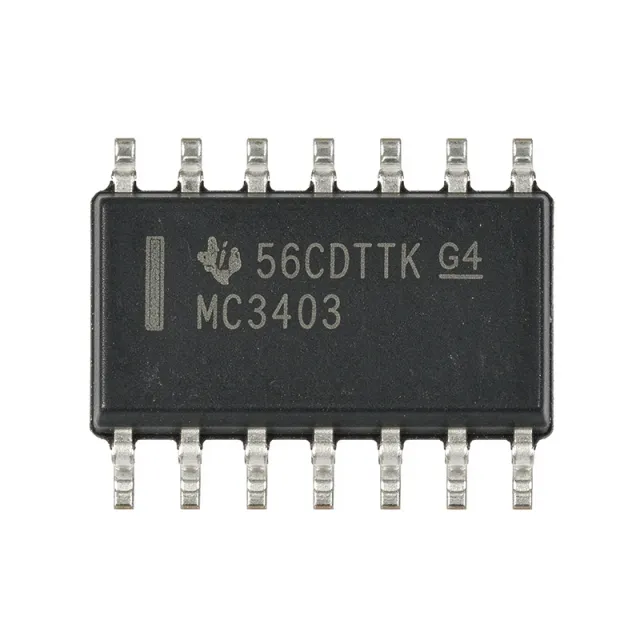
MC3403D - Quad 30 V 1 MHz Op Amp | Texas Instruments
MC3403D

MC3403D - Quad 30 V 1 MHz Op Amp | Texas Instruments

The Texas Instruments MC3403D is a quad, general-purpose bipolar operational amplifier built for single-supply and dual-supply analog systems. The device provides four amplifiers in a 14-SOIC package, operates from ±2.5 V to ±15 V according to the cited distributor specification, and supports a 1 MHz gain-bandwidth product. Its four-circuit integration reduces package count while providing true differential inputs and push-pull output capability. What is a quad operational amplifier? A quad operational amplifier combines four independent amplifier sections in one IC. These amplifiers serve as the active gain elements in sensors, buffers, analog filters, comparators, and feedback-control circuits. The MC3403 belongs to the operational-amplifier hierarchy, which is part of the broader amplifier-IC and signal-conditioning categories used in industrial control, instrumentation, audio, and communications equipment. Key verified features include four amplifier circuits, 1 MHz operation, 0.6 V/µs slew rate, a 14-pin SOIC package, and operation from −25 °C to 85 °C. The push-pull output stage supports bidirectional output-current drive in suitable loads, while the quad configuration gives designers four reusable analog channels in one package. These attributes make the MC3403D practical for low-to-moderate-frequency analog signal paths where four similar amplifier functions are required. The MC3403’s electrical characteristics are described as similar to the popular UA741 family, but its architecture is specifically useful in single-supply applications. Compared with a basic dual-supply-only op amp, the part offers a practical path to operating from a single rail in many circuits. Designers must still check input common-mode limits, output swing, supply current, noise, offset behavior, and stability against the manufacturer datasheet for the exact operating condition. Typical uses include sensor buffering, low-frequency active filtering, audio preamplification, transducers, analog control loops, and general instrumentation. For a new design, confirm the required input and output voltage ranges, acceptable slew rate, load impedance, noise performance, and temperature limits. For a replacement, verify the exact pinout, supply range, common-mode range, and output-swing requirements rather than relying only on the amplifier count. A key practical consideration is decoupling. Place the required supply bypass capacitors close to the power pins and keep sensitive input and feedback traces short. The MC3403D is a general-purpose amplifier, not a precision or high-speed device; use a more specialized amplifier when low offset, low noise, high speed, rail-to-rail operation, or extended temperature performance is mandatory. This page consolidates verified manufacturer and distributor information, drop-in alternatives, application guidance, package details, and selection considerations for engineers evaluating MC3403D. It is intended to support procurement and design review without substituting unsupported specifications for missing datasheet data.

USD $0,41 Em estoque