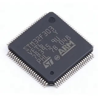
STM32F413VGT6 - 1MB Flash, 100MHz ARM Cortex-M4F MCU | STMicroelectronics
N.º da peça: STM32F413VGT6 ✓ Ativo| Qtd. | Preço unitário | Total |
|---|---|---|
| 1 | $12.5 | $12,50 |
| 10 | $11.25 | $112,50 |
| 100 | $10 | $1.000,00 |
| 500 | $9 | $4.500,00 |
| 1.000 | $8.1 | $8.100,00 |
STM32F413VGT6 Visão geral
What is a microcontroller? A microcontroller (MCU) is a compact integrated circuit designed to govern a specific operation in an embedded system. It integrates a processor core, memory (flash and SRAM), and programmable input/output peripherals on a single chip. Microcontrollers are the backbone of embedded systems, ranging from simple household appliances to complex industrial automation. The STM32F413VGT6 belongs to the STM32F4 series, which is part of the broader STM32 family of 32-bit ARM Cortex-M based MCUs. This hierarchy places it within the high-performance segment of the STM32 portfolio, offering a balance of processing power, memory, and peripheral integration.
Key features of the STM32F413VGT6 include a 100 MHz ARM Cortex-M4F core with FPU, 1 MB flash, 320 KB SRAM, and a comprehensive set of peripherals: multiple 12-bit ADCs, DACs, timers, communication interfaces (USART, SPI, I2C, CAN, USB OTG, SDIO), and a cryptographic acceleration unit. The device supports a wide supply voltage range of 1.7V to 3.6V and operates over a temperature range of -40°C to +85°C. It also includes a true random number generator (TRNG) and a real-time clock (RTC) for secure and time-sensitive applications.
Technically, the STM32F413VGT6 is built on a 90nm process technology, enabling high performance with low power consumption. The Cortex-M4F core includes a single-precision FPU and DSP instructions, accelerating mathematical computations for signal processing and control algorithms. The device features a memory protection unit (MPU) for enhanced security and reliability. With up to 100 MHz clock speed, it can execute complex algorithms efficiently, making it ideal for real-time control and data acquisition.
Typical applications include industrial control systems, motor drives, medical devices, consumer electronics, and IoT gateways. The rich peripheral set and large memory make it suitable for applications requiring connectivity (USB, CAN, Ethernet via external PHY) and advanced user interfaces. The cryptographic unit and TRNG enable secure communication protocols, essential for IoT security.
When designing with this device, ensure proper decoupling of the power supply pins with 100nF capacitors placed close to each VDD pin, and a 4.7uF bulk capacitor. The VDDA pin requires a dedicated analog supply with filtering to maintain ADC accuracy. The BOOT0 pin configuration determines the boot source; a pull-down resistor is recommended for normal flash boot. For high-speed USB, a 22-ohm series resistor on the USB D+ and D- lines is required.
Alternativas drop-in para STM32F413VGT6 — mesmo encapsulamento, compatível pino a pino. Peças de encapsulamento diferente que exigem retrabalho na PCB são excluídas.
Variantes desta série
Modelos da mesma série compatíveis como drop-in com STM32F413VGT6 (mesmo formato e footprint) — diferindo em Package, SRAM, Timers, ADC, Communication Interfaces.
Ferramenta de comparação rápida — selecione peças alternativas para comparação lado a lado:
STM32F413VGH6
✅ Drop-In ⚠️ Especificações não verificadas📋 Alternativa de referência (fora do catálogo)
STM32F413VGT6TR
✅ Drop-In ⚠️ Especificações não verificadas📋 Alternativa de referência (fora do catálogo)
STM32F407VGT6
✅ Drop-In ⚠️ Especificações não verificadas✓ Em estoque
$7.55 / unidade
Ver ficha técnica →STM32F415VGT6
✅ Drop-In ⚠️ Especificações não verificadas✓ Em estoque
$7.5 / unidade
Ver ficha técnica →STM32F417VGT6
✅ Drop-In ⚠️ Especificações não verificadas✓ Em estoque
$8.1 / unidade
Ver ficha técnica →LPC4357FET256
⚡ Mesmo encapsulamento ⚠️ Especificações não verificadas✓ Em estoque
$9.5 / unidade
Ver ficha técnica →STM32F413VGT6 Classificações máximas e características elétricas
| Core | ARM Cortex-M4F with FPU |
| Maximum Clock Speed | 100 MHz |
| Flash Memory | 1 MB |
| SRAM | 320 KB |
| Supply Voltage Range | 1.7 V to 3.6 V |
| Faixa de temperatura de operação | -40°C to +85°C |
| Encapsulamento | LQFP100 (14x14 mm, 0.5 mm pitch) |
| Número de pinos | 100 |
| ADC | 3x 12-bit, up to 16 channels |
| DAC | 2x 12-bit |
| Timers | 12x 16-bit, 2x 32-bit |
| Communication Interfaces | 6x USART, 5x SPI, 3x I2C, 2x CAN, USB OTG FS, SDIO |
| Cryptographic Acceleration | AES, DES, 3DES, SHA-1, SHA-256, MD5 |
| Random Number Generator | True RNG (TRNG) |
| DMA | 16-channel DMA controller |
| GPIO | Up to 82 I/O ports |
| Status RoHS | Compliant |
Configuração de pinos do STM32F413VGT6
| Pino 1 | PE2 — GPIO or alternate function |
| Pino 2 | PE3 — GPIO or alternate function |
| Pino 3 | PE4 — GPIO or alternate function |
| Pino 4 | PE5 — GPIO or alternate function |
| Pino 5 | PE6 — GPIO or alternate function |
| Pino 6 | VBAT — Backup battery supply |
| Pino 7 | PC13 — GPIO or RTC output |
| Pino 8 | PC14 — GPIO or OSC32_IN |
| Pino 9 | PC15 — GPIO or OSC32_OUT |
| Pino 10 | PF0 — GPIO or alternate function |
| Pino 11 | PF1 — GPIO or alternate function |
| Pino 12 | PF2 — GPIO or alternate function |
| Pino 13 | PF3 — GPIO or alternate function |
| Pino 14 | PF4 — GPIO or alternate function |
| Pino 15 | PF5 — GPIO or alternate function |
| Pino 16 | PF6 — GPIO or alternate function |
| Pino 17 | PF7 — GPIO or alternate function |
| Pino 18 | PF8 — GPIO or alternate function |
| Pino 19 | PF9 — GPIO or alternate function |
| Pino 20 | PF10 — GPIO or alternate function |
| Pino 21 | VSS — Ground |
| Pino 22 | VDD — Power supply |
| Pino 23 | PH0 — OSC_IN or GPIO |
| Pino 24 | PH1 — OSC_OUT or GPIO |
| Pino 25 | NRST — Reset (active low) |
| Pino 26 | PC0 — GPIO or ADC input |
| Pino 27 | PC1 — GPIO or ADC input |
| Pino 28 | PC2 — GPIO or ADC input |
| Pino 29 | PC3 — GPIO or ADC input |
| Pino 30 | VSSA — Analog ground |
| Pino 31 | VDDA — Analog power supply |
| Pino 32 | PA0 — GPIO or ADC input |
| Pino 33 | PA1 — GPIO or ADC input |
| Pino 34 | PA2 — GPIO or USART2_TX |
| Pino 35 | PA3 — GPIO or USART2_RX |
| Pino 36 | PA4 — GPIO or DAC_OUT1 |
| Pino 37 | PA5 — GPIO or DAC_OUT2 |
| Pino 38 | PA6 — GPIO or SPI1_MISO |
| Pino 39 | PA7 — GPIO or SPI1_MOSI |
| Pino 40 | PC4 — GPIO or I2S1_MCK |
| Pino 41 | PC5 — GPIO or I2S1_SCK |
| Pino 42 | PB0 — GPIO or ADC input |
| Pino 43 | PB1 — GPIO or ADC input |
| Pino 44 | PB2 — GPIO or BOOT1 |
| Pino 45 | PB10 — GPIO or I2C2_SCL |
| Pino 46 | PB11 — GPIO or I2C2_SDA |
| Pino 47 | PB12 — GPIO or SPI2_NSS |
| Pino 48 | PB13 — GPIO or SPI2_SCK |
| Pino 49 | PB14 — GPIO or SPI2_MISO |
| Pino 50 | PB15 — GPIO or SPI2_MOSI |
| Pino 51 | PD8 — GPIO or USART3_TX |
| Pino 52 | PD9 — GPIO or USART3_RX |
| Pino 53 | PD10 — GPIO or USART3_CK |
| Pino 54 | PD11 — GPIO or USART3_CTS |
| Pino 55 | PD12 — GPIO or USART3_RTS |
| Pino 56 | PD13 — GPIO or TIM4_CH2 |
| Pino 57 | PD14 — GPIO or TIM4_CH3 |
| Pino 58 | PD15 — GPIO or TIM4_CH4 |
| Pino 59 | PC6 — GPIO or TIM3_CH1 |
| Pino 60 | PC7 — GPIO or TIM3_CH2 |
| Pino 61 | PC8 — GPIO or TIM3_CH3 |
| Pino 62 | PC9 — GPIO or TIM3_CH4 |
| Pino 63 | PA8 — GPIO or USB_OTG_FS_SOF |
| Pino 64 | PA9 — GPIO or USB_OTG_FS_VBUS |
| Pino 65 | PA10 — GPIO or USB_OTG_FS_ID |
| Pino 66 | PA11 — GPIO or USB_OTG_FS_DM |
| Pino 67 | PA12 — GPIO or USB_OTG_FS_DP |
| Pino 68 | PA13 — GPIO or SWDIO |
| Pino 69 | PA14 — GPIO or SWCLK |
| Pino 70 | PA15 — GPIO or JTDI |
| Pino 71 | PC10 — GPIO or USART4_TX |
| Pino 72 | PC11 — GPIO or USART4_RX |
| Pino 73 | PC12 — GPIO or USART5_TX |
| Pino 74 | PD0 — GPIO or CAN1_RX |
| Pino 75 | PD1 — GPIO or CAN1_TX |
| Pino 76 | PD2 — GPIO or TIM3_ETR |
| Pino 77 | PD3 — GPIO or USART2_CTS |
| Pino 78 | PD4 — GPIO or USART2_RTS |
| Pino 79 | PD5 — GPIO or USART2_TX |
| Pino 80 | PD6 — GPIO or USART2_RX |
| Pino 81 | PD7 — GPIO or USART2_CK |
| Pino 82 | PE7 — GPIO or TIM1_ETR |
| Pino 83 | PE8 — GPIO or TIM1_CH1 |
| Pino 84 | PE9 — GPIO or TIM1_CH2 |
| Pino 85 | PE10 — GPIO or TIM1_CH3 |
| Pino 86 | PE11 — GPIO or TIM1_CH4 |
| Pino 87 | PE12 — GPIO or TIM1_CH1N |
| Pino 88 | PE13 — GPIO or TIM1_CH2N |
| Pino 89 | PE14 — GPIO or TIM1_CH3N |
| Pino 90 | PE15 — GPIO or TIM1_CH4N |
| Pino 91 | PB3 — GPIO or JTDO |
| Pino 92 | PB4 — GPIO or NJTRST |
| Pino 93 | PB5 — GPIO or I2C1_SMBA |
| Pino 94 | PB6 — GPIO or I2C1_SCL |
| Pino 95 | PB7 — GPIO or I2C1_SDA |
| Pino 96 | BOOT0 — Boot mode selection |
| Pino 97 | PB8 — GPIO or CAN2_RX |
| Pino 98 | PB9 — GPIO or CAN2_TX |
| Pino 99 | VSS — Ground |
| Pino 100 | VDD — Power supply |
Aplicações típicas
STM32F413VGT6 é adequado para 6 aplicaçãos: Industrial Control Systems, Medical Devices, IoT Gateways, Consumer Electronics, Automotive Electronics, Test and Measurement Equipment.
Industrial Control Systems
The STM32F413VGT6 is ideal for industrial control systems due to its high-speed 100 MHz Cortex-M4F core, multiple timers for PWM generation, and 12-bit ADCs for precise analog sensing. It can handle complex control algorithms like PID and FOC for motor drives, and its robust communication interfaces (CAN, USART, SPI) enable seamless integration with industrial networks. The device's wide operating temperature range (-40°C to +85°C) ensures reliability in harsh environments. In a typical PLC (Programmable Logic Controller), the STM32F413VGT6 manages I/O scanning, communication protocols, and real-time control loops. Its 1 MB flash allows storing extensive firmware for multiple functions, while 320 KB SRAM supports large data buffers for data logging. The cryptographic unit enhances security for industrial IoT applications, protecting against unauthorized access. Designers can leverage the STM32CubeMX tool to configure peripherals and generate initialization code, accelerating development. The LQFP100 package is easy to solder and suitable for industrial PCBs with moderate component density.
Recomendado
Medical Devices
The STM32F413VGT6 is well-suited for medical devices such as patient monitors, infusion pumps, and diagnostic equipment. Its high processing power enables real-time signal processing for ECG, EEG, and blood pressure monitoring. The device's low power consumption is critical for battery-operated portable medical devices, and its wide voltage range (1.7V to 3.6V) allows operation from a single lithium-ion cell. The cryptographic acceleration unit ensures secure data transmission for patient privacy compliance (e.g., HIPAA). In a typical patient monitor, the STM32F413VGT6 acquires analog signals from sensors via its ADCs, processes them using DSP instructions, and displays results on an LCD. The 1 MB flash stores calibration data and firmware updates, while 320 KB SRAM buffers real-time data streams. The device's multiple communication interfaces (USB, UART, SPI) facilitate connectivity to external modules like Wi-Fi or Bluetooth for remote monitoring. The LQFP100 package is compact enough for portable designs, and the -40°C to +85°C temperature range covers clinical environments. Designers must ensure proper isolation and EMC compliance for medical safety standards.
Recomendado
IoT Gateways
The STM32F413VGT6 is an excellent choice for IoT gateways that aggregate data from multiple sensors and communicate with cloud services. Its rich connectivity options (USB OTG, CAN, SDIO, USART, SPI, I2C) allow interfacing with various wireless modules (Wi-Fi, LoRa, Zigbee) and wired networks. The cryptographic acceleration unit enables secure TLS/DTLS handshakes, essential for protecting data in transit. The device's 100 MHz core can handle protocol stacks like MQTT and CoAP efficiently. In a typical IoT gateway, the STM32F413VGT6 collects sensor data via UART or SPI, processes it locally, and forwards it to the cloud via an Ethernet or Wi-Fi module. The 1 MB flash stores the firmware and configuration, while 320 KB SRAM buffers data bursts. The TRNG generates secure keys for authentication. The device's low-power modes allow battery-powered gateways to operate for extended periods. The LQFP100 package is suitable for compact gateway designs, and the wide temperature range supports outdoor deployment. Designers should consider adding an external Ethernet PHY for wired connectivity, as the F413 does not have a built-in MAC.
Recomendado
Consumer Electronics
The STM32F413VGT6 is used in high-end consumer electronics like smart home hubs, audio systems, and wearable devices. Its high performance enables advanced user interfaces with graphics, audio processing, and voice recognition. The device's large memory (1 MB flash, 320 KB SRAM) supports complex applications and over-the-air updates. The cryptographic unit ensures secure firmware updates and user data protection. In a smart home hub, the STM32F413VGT6 manages multiple communication protocols (Zigbee, Z-Wave, Wi-Fi) and controls connected devices. Its ADCs and DACs interface with sensors and audio codecs. The device's low power consumption is crucial for battery-powered wearables, and its small LQFP100 package fits compact designs. The -40°C to +85°C temperature range covers typical consumer environments. Designers can use STM32CubeMX to configure peripherals and generate code, speeding up development. For audio applications, the FPU accelerates audio processing algorithms like noise cancellation and equalization.
Recomendado
Automotive Electronics
The STM32F413VGT6 is suitable for automotive applications such as body control modules, infotainment systems, and advanced driver-assistance systems (ADAS) entry-level. Its high performance and rich peripherals enable real-time control and communication with CAN buses. The device's wide temperature range (-40°C to +85°C) meets automotive requirements, and its cryptographic unit supports secure communication protocols like SecOC. In a body control module, the STM32F413VGT6 manages lighting, windows, and door locks, using its timers for PWM dimming and ADCs for sensor inputs. The CAN interface connects to the vehicle's network. The 1 MB flash stores complex diagnostic routines, and 320 KB SRAM handles real-time data. The device's low power consumption is beneficial for always-on modules. The LQFP100 package is robust for automotive PCBs. Designers must ensure compliance with AEC-Q100 standards; the standard STM32F413VGT6 is not AEC-Q100 qualified, but ST offers automotive-grade variants (e.g., STM32F413VGT6Q) for such applications.
Recomendado
Test and Measurement Equipment
The STM32F413VGT6 is ideal for test and measurement equipment like oscilloscopes, data loggers, and signal generators. Its high-speed ADC and DACs enable precise signal acquisition and generation. The 100 MHz core can handle real-time signal processing, and the large memory buffers data for analysis. The device's multiple timers provide accurate timebase for triggering and sampling. In a portable oscilloscope, the STM32F413VGT6 acquires analog signals via its ADCs, processes them using DSP instructions, and displays waveforms on an LCD. The 1 MB flash stores firmware and calibration data, while 320 KB SRAM buffers waveform samples. The USB OTG interface allows connection to a PC for data transfer. The device's low power consumption extends battery life in portable instruments. The LQFP100 package is suitable for compact designs. Designers can use the FPU for fast FFT computations. The wide temperature range ensures accuracy in various environments.
Recomendado
Resumo dos produtos recomendados
Dados de referência de engenharia para STM32F413VGT6 — comparação, orientação de projeto e informações de conformidade.
Guia de seleção
Comparação com alternativas
| Parâmetro | Este produto | STM32F413VGH6 | STM32F407VGT6 | STM32F415VGT6 | STM32F417VGT6 | LPC4357FET256 |
|---|---|---|---|---|---|---|
| Package | LQFP100 | LQFP100 - same | LQFP100 - same | LQFP100 - same | LQFP100 - same | LQFP100 - same |
| Brand | STMicroelectronics | STMicroelectronics | STMicroelectronics | STMicroelectronics | STMicroelectronics | NXP Semiconductors |
| Core | ARM Cortex-M4F | ARM Cortex-M4F | ARM Cortex-M4F | ARM Cortex-M4F | ARM Cortex-M4F | Dual-core Cortex-M4/M0 |
| Maximum Clock Speed | 100 MHz | 100 MHz | 168 MHz | 100 MHz | 168 MHz | 204 MHz (M4) |
| Flash Memory | 1 MB | 1 MB | 1 MB | 1 MB | 1 MB | 1 MB |
| SRAM | 320 KB | 320 KB | 192 KB | 192 KB | 192 KB | 136 KB |
| Cryptographic Acceleration | Yes (AES, DES, 3DES, SHA-1, SHA-256, MD5) | Yes | No | No | No | No |
| Ethernet MAC | No | No | Yes | No | Yes | Yes |
| Temperature Range | -40°C to +85°C | -40°C to +105°C | -40°C to +85°C | -40°C to +85°C | -40°C to +85°C | -40°C to +85°C |
Principais diferenciais
- Largest SRAM in its class (320 KB) (vs STM32F407VGT6)
- Integrated cryptographic acceleration (vs STM32F407VGT6)
- Lower power consumption at same clock (vs STM32F407VGT6)
Notas de projeto
Decouple each VDD pin with a 100nF ceramic capacitor placed as close as possible to the pin. Additionally, place a 4.7uF bulk capacitor on the main VDD rail. The VDDA pin must be connected to a clean analog supply, typically through a ferrite bead and a 1uF capacitor to ground, to ensure ADC accuracy. The VBAT pin should be connected to a backup battery or tied to VDD through a diode to maintain RTC operation when main power is off.
For high-speed USB, route the D+ and D- lines as a differential pair with 90-ohm impedance. Place a 22-ohm series resistor on each line near the MCU. For the crystal oscillator, place the crystal and load capacitors close to the OSC_IN/OSC_OUT pins, and keep the trace lengths short to minimize parasitic capacitance. Use a ground plane under the MCU to reduce noise and improve EMC.
Ensure the BOOT0 pin is pulled low (through a 10k resistor) for normal flash boot. If BOOT0 is high, the device will boot from system memory, which may cause unexpected behavior. Also, do not leave unused GPIO pins floating; configure them as outputs or enable internal pull-ups/pull-downs to avoid excessive power consumption. For ADC accuracy, avoid routing digital signals near the VDDA pin.
Informações de conformidade
RoHS compliant per STMicroelectronics. Not AEC-Q100 qualified; automotive-grade variant STM32F413VGT6Q is available.