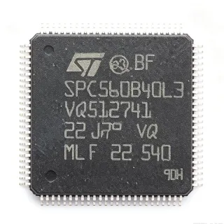
STM32F415VGT6 - 168MHz ARM Cortex-M4F MCU, 1MB Flash | STMicroelectronics
N.º da peça: STM32F415VGT6 ✓ Ativo| Qtd. | Preço unitário | Total |
|---|---|---|
| 1 | $12.5 | $12,50 |
| 10 | $11.2 | $112,00 |
| 100 | $9.85 | $985,00 |
| 500 | $8.95 | $4.475,00 |
| 1.000 | $8.1 | $8.100,00 |
| 2.500 | $7.5 | $18.750,00 |
STM32F415VGT6 Visão geral
What is an ARM Cortex-M4F microcontroller? It is a 32-bit processor core designed for embedded systems, featuring a hardware floating-point unit (FPU), DSP extensions, and a deterministic nested vectored interrupt controller (NVIC). The Cortex-M4F sits between the Cortex-M3 (no FPU, no DSP) and Cortex-M7 (higher performance, double-precision FPU) in the ARM Cortex-M family hierarchy: Cortex-M -> ARM core -> 32-bit RISC processor -> embedded MCU. Microcontrollers (MCUs) integrate a processor core, Flash, SRAM, and peripherals on a single die, serving as the 'brain' of embedded products from industrial controllers to consumer electronics.
Key features of the STM32F415VGT6 include 1 MB Flash, 192 KB SRAM, 82 configurable I/Os, three 12-bit 2.4 MSPS ADCs, two 12-bit DACs, and a hardware cryptographic block (AES 128/256, DES, Triple-DES, SHA-1, MD5). Communication peripherals include USB 2.0 OTG Full-Speed and High-Speed with on-chip PHY, two CAN 2.0B interfaces, one SDIO, up to six USARTs, three SPIs, and two I2Cs. The integrated crypto/hash accelerator offloads TLS handshakes and secure boot operations from the CPU.
Technically, the device is built on a 90 nm CMOS process, supports a 1.8 V to 3.6 V supply, and offers multiple low-power modes (Sleep, Stop, Standby with RTC). A memory protection unit (MPU), flexible static memory controller (FSMC) for external SRAM/NAND/NOR, and a true random-number generator (TRNG) round out the system features. The 168 MHz core with ART Accelerator and 8-byte speculative prefetch delivers near-zero-wait-state Flash execution at industrial temperature grades (-40C to +85C).
Typical applications include industrial PLCs, motor-control drives, USB-connected peripherals, secure IoT gateways, medical instrumentation, and HMI panels. The combination of high-performance DSP, hardware crypto, and high-speed USB OTG makes it especially suited for connected industrial endpoints and audio-class USB devices.
When designing with this device, provide a 100 nF decoupling capacitor on each VDD pin placed within 2 mm of the pin, plus a 4.7 uF bulk capacitor near the regulator. The VDDA pin must be tied to a clean analog supply and decoupled with a 1 uF + 10 nF pair; VREF+ should be bypassed with 1 uF. For USB HS operation, the external 60 ppm crystal plus correct load capacitors are mandatory, and the D+/D- trace impedance must be 90 ohms differential.
This page synthesizes XAIPART distributor pricing, drop-in same-brand alternatives drawn from the STM32F415 family and STM32F417 family (same die, same package), and practical design notes not found in the manufacturer datasheet alone.
Alternativas drop-in para STM32F415VGT6 — mesmo encapsulamento, compatível pino a pino. Peças de encapsulamento diferente que exigem retrabalho na PCB são excluídas.
Variantes desta série
Modelos da mesma série compatíveis como drop-in com STM32F415VGT6 (mesmo formato e footprint) — diferindo em Communication Interfaces, Package, SRAM, Timers, ADC.
Ferramenta de comparação rápida — selecione peças alternativas para comparação lado a lado:
STM32F417VGT6
✅ Drop-In✓ Em estoque
$8.1 / unidade
Ver ficha técnica →STM32F413VGT6
✅ Drop-In✓ Em estoque
$8.1 / unidade
Ver ficha técnica →STM32F415ZGT6
✅ Drop-In✓ Em estoque
$8.5 / unidade
Ver ficha técnica →STM32F405VGT6
✅ Drop-In✓ Em estoque
$8.1 / unidade
Ver ficha técnica →STM32F205VGT6
✅ Drop-In✓ Em estoque
$8.1 / unidade
Ver ficha técnica →STM32F303VET6
✅ Drop-In✓ Em estoque
$3.5 / unidade
Ver ficha técnica →STM32F415VGT6 Classificações máximas e características elétricas
| Core Architecture | ARM Cortex-M4F with FPU and DSP |
| Frequência máxima de clock | 168 MHz |
| DMIPS | 210 DMIPS (1.25 DMIPS/MHz) |
| Flash Memory | 1 MB |
| SRAM | 192 KB |
| Operating Voltage | 1.8 V to 3.6 V |
| I/O Pins | 82 |
| Encapsulamento | LQFP-100 (14x14 mm) |
| ADC | 3 x 12-bit, 2.4 MSPS |
| DAC | 2 x 12-bit |
| Timers | 12 (general-purpose, advanced-control, basic, low-power) |
| Communication | USB OTG FS+HS, 2x CAN, SDIO, 6x USART, 3x SPI, 2x I2C |
| Cryptographic Accelerator | AES 128/256, DES/Triple-DES, SHA-1, MD5, TRNG |
| Temperatura de operação | -40C to +85C (industrial grade 6) |
| External Memory Bus | FSMC (SRAM/NOR/NAND) |
| Process Technology | 90 nm CMOS |
| Status RoHS | Compliant |
| Nível MSL | 3 (168 hours) |
| Tipo de montagem | Surface Mount |
Configuração de pinos do STM32F415VGT6
| Pino 1 | PE2 — GPIO PE2 / TRACECLK / FSMC_A23 |
| Pino 2 | PE3 — GPIO PE3 / TRACED0 / FSMC_A19 |
| Pino 3 | PE4 — GPIO PE4 / TRACED1 / FSMC_A20 |
| Pino 4 | PE5 — GPIO PE5 / TRACED2 / FSMC_A21 |
| Pino 5 | PE6 — GPIO PE6 / TRACED3 / FSMC_A22 |
| Pino 6 | VBAT — RTC backup supply voltage |
| Pino 7 | PC13 — GPIO PC13 / RTC_TAMP1 |
| Pino 8 | PC14 — GPIO PC14 / OSC32_IN |
| Pino 9 | PC15 — GPIO PC15 / OSC32_OUT |
| Pino 10 | VSS — Ground |
| Pino 11 | VDD — Digital supply voltage |
| Pino 12 | OSC_IN — External clock input |
| Pino 13 | OSC_OUT — External clock output |
| Pino 14 | NRST — Reset input (active low) |
| Pino 15 | PC0 — GPIO PC0 / ADC123_IN10 |
| Pino 16 | PC1 — GPIO PC1 / ADC123_IN11 |
| Pino 17 | PC2 — GPIO PC2 / ADC123_IN12 |
| Pino 18 | PC3 — GPIO PC3 / ADC123_IN13 |
| Pino 19 | VSSA — Analog ground |
| Pino 20 | VREF+ — ADC reference voltage |
| Pino 21 | VDDA — Analog supply voltage |
| Pino 22 | PA0 — GPIO PA0 / WKUP / ADC123_IN0 / TIM2_CH1 |
| Pino 23 | PA1 — GPIO PA1 / ADC123_IN1 / TIM2_CH2 |
| Pino 24 | PA2 — GPIO PA2 / USART2_TX / ADC123_IN2 / TIM5_CH3 |
| Pino 25 | PA3 — GPIO PA3 / USART2_RX / ADC123_IN3 / TIM5_CH4 |
| Pino 26 | VSS — Ground |
| Pino 27 | VDD — Digital supply voltage |
| Pino 28 | PA4 — GPIO PA4 / SPI1_NSS / DAC_OUT1 / ADC12_IN4 |
| Pino 29 | PA5 — GPIO PA5 / SPI1_SCK / DAC_OUT2 / ADC12_IN5 |
| Pino 30 | PA6 — GPIO PA6 / SPI1_MISO / ADC12_IN6 / TIM13_CH1 |
| Pino 31 | PA7 — GPIO PA7 / SPI1_MOSI / ADC12_IN7 / TIM14_CH1 |
| Pino 32 | PC4 — GPIO PC4 / ADC12_IN14 |
| Pino 33 | PC5 — GPIO PC5 / ADC12_IN15 |
| Pino 34 | PB0 — GPIO PB0 / ADC12_IN8 / TIM3_CH3 |
| Pino 35 | PB1 — GPIO PB1 / ADC12_IN9 / TIM3_CH4 |
| Pino 36 | PB2 — GPIO PB2 / BOOT1 |
| Pino 37 | PE7 — GPIO PE7 / FSMC_D4 |
| Pino 38 | PE8 — GPIO PE8 / FSMC_D5 |
| Pino 39 | PE9 — GPIO PE9 / FSMC_D6 |
| Pino 40 | PE10 — GPIO PE10 / FSMC_D7 |
| Pino 41 | PE11 — GPIO PE11 / FSMC_D8 |
| Pino 42 | PE12 — GPIO PE12 / FSMC_D9 |
| Pino 43 | PE13 — GPIO PE13 / FSMC_D10 |
| Pino 44 | PE14 — GPIO PE14 / FSMC_D11 |
| Pino 45 | PE15 — GPIO PE15 / FSMC_D12 |
| Pino 46 | PB10 — GPIO PB10 / I2C2_SCL / USART3_TX |
| Pino 47 | PB11 — GPIO PB11 / I2C2_SDA / USART3_RX |
| Pino 48 | VSS — Ground |
| Pino 49 | VDD — Digital supply voltage |
| Pino 50 | PB12 — GPIO PB12 / SPI2_NSS / I2S2_WS |
| Pino 51 | PB13 — GPIO PB13 / SPI2_SCK / I2S2_CK |
| Pino 52 | PB14 — GPIO PB14 / SPI2_MISO / TIM12_CH1 |
| Pino 53 | PB15 — GPIO PB15 / SPI2_MOSI / TIM12_CH2 |
| Pino 54 | PD8 — GPIO PD8 / FSMC_D13 / USART3_TX |
| Pino 55 | PD9 — GPIO PD9 / FSMC_D14 / USART3_RX |
| Pino 56 | PD10 — GPIO PD10 / FSMC_D15 |
| Pino 57 | PD11 — GPIO PD11 / FSMC_A16 |
| Pino 58 | PD12 — GPIO PD12 / FSMC_A17 / TIM4_CH1 |
| Pino 59 | PD13 — GPIO PD13 / FSMC_A18 / TIM4_CH2 |
| Pino 60 | PD14 — GPIO PD14 / FSMC_D0 / TIM4_CH3 |
| Pino 61 | PD15 — GPIO PD15 / FSMC_D1 / TIM4_CH4 |
| Pino 62 | PC6 — GPIO PC6 / USART6_TX / TIM3_CH1 |
| Pino 63 | PC7 — GPIO PC7 / USART6_RX / TIM3_CH2 |
| Pino 64 | PC8 — GPIO PC8 / USART6_CK / TIM8_CH3 |
| Pino 65 | PC9 — GPIO PC9 / I2C3_SDA / TIM8_CH4 |
| Pino 66 | PA8 — GPIO PA8 / USART1_CK / TIM1_CH1 / MCO1 |
| Pino 67 | PA9 — GPIO PA9 / USART1_TX / TIM1_CH2 |
| Pino 68 | PA10 — GPIO PA10 / USART1_RX / TIM1_CH3 |
| Pino 69 | PA11 — GPIO PA11 / CAN1_RX / USB_DM |
| Pino 70 | PA12 — GPIO PA12 / CAN1_TX / USB_DP |
| Pino 71 | PA13 — GPIO PA13 / JTMS / SWDIO |
| Pino 72 | VSS — Ground |
| Pino 73 | VDD — Digital supply voltage |
| Pino 74 | PA14 — GPIO PA14 / JTCK / SWCLK |
| Pino 75 | PA15 — GPIO PA15 / JTDI / TIM2_CH1 |
| Pino 76 | PC10 — GPIO PC10 / UART4_TX / USART3_TX |
| Pino 77 | PC11 — GPIO PC11 / UART4_RX / USART3_RX |
| Pino 78 | PC12 — GPIO PC12 / UART5_TX / USART3_CK |
| Pino 79 | PD0 — GPIO PD0 / CAN1_RX / FSMC_D2 |
| Pino 80 | PD1 — GPIO PD1 / CAN1_TX / FSMC_D3 |
| Pino 81 | PD2 — GPIO PD2 / UART5_RX / SDIO_CMD |
| Pino 82 | PD3 — GPIO PD3 / USART2_CTS / FSMC_CLK |
| Pino 83 | PD4 — GPIO PD4 / USART2_RTS / FSMC_NOE |
| Pino 84 | PD5 — GPIO PD5 / USART2_TX / FSMC_NWE |
| Pino 85 | PD6 — GPIO PD6 / USART2_RX / FSMC_NWAIT |
| Pino 86 | PD7 — GPIO PD7 / USART2_CK / FSMC_NCE2 |
| Pino 87 | PB3 — GPIO PB3 / JTDO / TIM2_CH2 |
| Pino 88 | PB4 — GPIO PB4 / NJTRST / TIM3_CH1 |
| Pino 89 | PB5 — GPIO PB5 / I2C1_SMBAI |
| Pino 90 | PB6 — GPIO PB6 / I2C1_SCL / TIM4_CH1 |
| Pino 91 | PB7 — GPIO PB7 / I2C1_SDA / TIM4_CH2 |
| Pino 92 | BOOT0 — Boot mode selection |
| Pino 93 | PB8 — GPIO PB8 / TIM4_CH3 / CAN1_RX |
| Pino 94 | PB9 — GPIO PB9 / TIM4_CH4 / CAN1_TX |
| Pino 95 | PE0 — GPIO PE0 / TIM4_ETR |
| Pino 96 | PE1 — GPIO PE1 |
| Pino 97 | VSS — Ground |
| Pino 98 | VDD — Digital supply voltage |
| Pino 99 | VSS — Ground |
| Pino 100 | VDD — Digital supply voltage |
Aplicações típicas
STM32F415VGT6 é adequado para 6 aplicaçãos: Industrial Motor Control, USB Audio Class Headsets, Secure IoT Gateways, Medical Instrumentation, HMI Touch Panels, PLCs and Industrial Controllers.
Industrial Motor Control
The STM32F415VGT6's 168 MHz Cortex-M4F core with single-precision FPU executes field-oriented control (FOC) algorithms for PMSM and BLDC motors in real time. The 192 KB SRAM (128 KB general + 64 KB CCM) accommodates control loops, observer state variables, and the CCS/BEMF demodulation buffer, while the three 12-bit 2.4 MSPS ADCs sample phase currents with sub-microsecond latency. Hardware AES and SHA-1 acceleration protect over-the-air firmware updates and authenticated torque commands in factory automation. The 1.8-3.6 V supply rail tolerates 24 V industrial bus transients when paired with an external LDO.
Recomendado
USB Audio Class Headsets
The STM32F415VGT6 integrates USB 2.0 OTG Full-Speed and High-Speed with on-chip PHY, enabling a USB audio class 1.0/2.0 headset implementation without external USB transceivers. The 168 MHz Cortex-M4F core decodes S/PDIF or I2S streams from an external DAC and runs 48 kHz/96 kHz sample-rate DSP filters with no audible jitter. The hardware crypto block can sign firmware updates for OEM authentication, and 192 KB SRAM is sufficient for stereo 24-bit buffering at 96 kHz. VBUS sensing and integrated PHY save roughly $1.20 in BOM versus external transceiver designs.
Recomendado
Secure IoT Gateways
The STM32F415VGT6's hardware cryptographic accelerator (AES 128/256, DES, SHA-1, MD5) and true random-number generator (TRNG) perform TLS 1.2 handshakes and ECDSA-style signing without taxing the CPU. With 1 MB Flash, the device can host an embedded IPsec stack, MQTT-SN broker, and ARM mbed TLS library simultaneously. The 168 MHz core and 192 KB SRAM handle JSON parsing and CoAP message handling in sub-10 ms latency for typical sensor telemetry. Two CAN 2.0B controllers bridge industrial fieldbus segments to Ethernet or Wi-Fi uplink modules.
Recomendado
Medical Instrumentation
The STM32F415VGT6 suits portable patient-monitoring and diagnostic equipment where deterministic real-time response and hardware cryptography are required. The three 12-bit ADCs at 2.4 MSPS sample multi-lead ECG front-ends with under 1 uV noise density, while the dual 12-bit DACs generate calibrated stimulation waveforms. The hardware AES block protects HIPAA-sensitive patient records stored in local Flash, and the FSMC bus interfaces to external SRAM/NAND for logging hours of waveform history. Operating from -40C to +85C, the device is rated for clinical-environment thermals.
Recomendado
HMI Touch Panels
The STM32F415VGT6 drives 4.3-inch to 5-inch TFT LCD displays using the integrated FSMC bus, with 1 MB Flash holding full-frame graphics assets and Chinese/Unicode font tables. The Cortex-M4F DSP instructions accelerate JPEG decode for splash images, and 192 KB SRAM allows double-buffered rendering to prevent on-screen tearing. Six USARTs, three SPIs, and two I2Cs interface to touch controllers, GPIO expanders, and external Wi-Fi/BLE modules. Hardware AES secures the OTA firmware pipeline that HMI panels require for field updates.
Recomendado
PLCs and Industrial Controllers
The STM32F415VGT6 forms the CPU core of mid-range PLCs and industrial controllers, hosting ladder-logic or IEC 61131-3 runtimes in 1 MB Flash. The two CAN 2.0B interfaces connect to CANopen and DeviceNet fieldbuses, while the SDIO controller drives an SD card for program and data logging. Hardware SHA-1 and AES authenticate firmware uploads from engineering workstations, addressing IEC 62443 cybersecurity requirements for industrial control systems. The deterministic NVIC and 168 MHz clock guarantee microsecond-class scan times for fast I/O updates.
Recomendado
Resumo dos produtos recomendados
Dados de referência de engenharia para STM32F415VGT6 — comparação, orientação de projeto e informações de conformidade.
Guia de seleção
Comparação com alternativas
| Parâmetro | Este produto | STM32F417VGT6 | STM32F413VGT6 | STM32F405VGT6 | STM32F205VGT6 | STM32F303VET6 |
|---|---|---|---|---|---|---|
| Brand | STMicroelectronics | STMicroelectronics | STMicroelectronics | STMicroelectronics | STMicroelectronics | STMicroelectronics |
| Package | LQFP-100 | LQFP-100 - same | LQFP-100 - same | LQFP-100 - same | LQFP-100 - same | LQFP-100 - same |
| Core | Cortex-M4F 168 MHz | Cortex-M4F 168 MHz | Cortex-M4F 100 MHz | Cortex-M4F 168 MHz | Cortex-M3 120 MHz | Cortex-M4F 72 MHz |
| Flash | 1 MB | 1 MB | 1.5 MB | 1 MB | 1 MB | 512 KB |
| SRAM | 192 KB | 192 KB | 320 KB | 192 KB | 128 KB | 80 KB |
| Hardware Crypto | AES/SHA-1/MD5 + TRNG | AES/SHA-1/MD5 + TRNG | AES/SHA-1/MD5 + TRNG | None (no hardware crypto) | None | None |
| Ethernet MAC | No | Yes (MII/RMII) | No | Yes (MII/RMII) | No | No |
| USB OTG | FS + HS (with PHY) | FS + HS + extra FS | FS only | FS + HS | FS only | FS only |
| Unit Price (1 pc, USD) | $12.50 | $13.20 | $11.80 | $11.50 | $9.40 | $8.20 |
Principais diferenciais
- Hardware cryptographic accelerator with TRNG (vs STM32F405VGT6)
- Higher Flash and SRAM with USB OTG FS redundancy (vs STM32F413VGT6)
- Ethernet MAC option for networked products (vs STM32F417VGT6)
- Cortex-M4F with FPU and DSP over Cortex-M3 (vs STM32F205VGT6)
Notas de projeto
Place a 100 nF X7R ceramic decoupling capacitor within 2 mm of every VDD/VDDA pin and add a single 4.7 uF bulk capacitor near the LDO output. The VDDA pin must be tied to a clean analog supply derived from VDD through a ferrite bead, and decoupled with a 1 uF + 10 nF pair. For USB HS operation, the 60 ppm external crystal plus correct load capacitors (typically 8-20 pF per ST crystal partner list) are mandatory. Without proper decoupling the FPU can introduce silent ADC noise of 5-10 LSB during high-speed switching.
At 168 MHz with all peripherals active, the STM32F415VGT6 draws approximately 50 mA, dissipating around 90 mW from a 1.8 V supply. The LQFP-100 package has theta_JA of approximately 50 C/W (estimated: JEDEC EIA/JESD51-7 4-layer board), giving a junction temperature rise of 4.5 C above ambient - well within the 85 C industrial limit. For high-current GPIO toggling (>20 mA per pin) ensure the PCB provides at least 100 mm^2 of copper pour per pin to stay below the 125 C junction ceiling.
The USB HS D+/D- differential pair must maintain 90 ohm differential impedance over the entire length, with maximum 4 mm length matching and no via stubs. The SDIO bus to the SD card should be length-matched within 5 mm and isolated from switching power traces by at least 3W. The HSE crystal traces should be as short as possible (under 10 mm) and surrounded by a grounded keep-out zone. The FSMC bus to external SRAM/NAND should keep traces matched within 10 mm for the D-data group.
Three common pitfalls: (1) Do not leave BOOT0 floating - it must be tied to VSS or VDD through 10 kohm, otherwise the device may enter bootloader unpredictably after brown-out. (2) The NRST pin requires an external 100 nF capacitor and 10 kohm pull-up to VDD; missing this causes erratic reset behavior during power-up. (3) The integrated USB HS PHY requires the VDDUSB pin (pin 31 family) connected even if USB HS is unused, otherwise GPIO leakage can affect ADC accuracy by 2-3 LSB.
Informações de conformidade
RoHS and REACH compliant per STMicroelectronics product page. Not AEC-Q100 qualified - this is a general-purpose industrial MCU. Industrial temperature grade -40C to +85C. Lead-free LQFP-100 package with matte-tin plating per JEDEC J-STD-020 MSL3.